High-throughput nanopore fabrication and classification using FIB irradiation and automated pore edge analysis
Abstract
Large-area nanopore drilling is a major bottleneck in state-of-the-art nanoporous 2D membrane fabrication protocols. In addition, high-quality structural and statistical descriptions of as-fabricated porous membranes are key to predicting the corresponding membrane-wide permeation properties. In this work, we investigate Xe-ion focused ion beam as a tool for scalable, large-area nanopore fabrication on atomically thin, free-standing molybdenum disulphide. The presented irradiation protocol enables designing ultrathin membranes with tunable porosity and pore dimension, along with spatial uniformity across large-area substrates. Fabricated nanoporous membranes were characterized using scanning transmission electron microscopy imaging and the observed nanopore geometries were analyzed through a pore-edge detection script. We further demonstrated that the obtained structural and statistical data can be readily passed on to computational and analytical tools to predict the permeation properties at both individual pore and membrane-wide scales. As an example, membranes featuring angstrom-scale pores were investigated in terms of their emerging water and ion flow properties through extensive all-atom molecular dynamics simulations. We believe that the combination of experimental and analytical approaches presented here should yield accurate physics-based property estimates and thus potentially enable a true function-by-design approach to fabrication for applications such as osmotic power generation, desalination/filtration, as well as their strain-tunable versions.
Keywords nanopore MoS2 FIB Xe PFIB nanofluidics osmotic power generation desalination
1 Introduction
Defect engineering is an important tool for enabling and exploring various physical phenomena at the nanoscale. From electronics [1] and spintronics [2] to optical [3, 4, 5] applications, the control over the material’s crystal lattice structure is paramount to pushing the boundaries of modern technology [6, 7, 8]. Atomically thin materials are especially interesting, as they also promise to become the next-generation porous membranes for desalination [9, 10], gas filtration [11], energy generation [12], optoelectronics [13], biosensing [14, 15, 16, 17], and mechanosensing [18, 19, 20, 21] applications. In these areas, defect engineering is used to fabricate nanometer-scale defects or pores. With atomically thin and van der Waals materials such as graphene or molybdenum disulphide (MoS2) as host membranes, the membrane thickness can also be controlled during fabrication. By tuning the size, pore-edge termination, and pore density, one possesses sensitive control over the membrane properties such as ion selectivity [22] and water permeability [23], making the level of precision in controlling the geometry and composition of the fabricated defects (nanopores) a crucial fabrication component [12].
Among the numerous available nanopore fabrication methods [12, 24, 25], the electron beam [26] and ion irradiation [27] techniques offer a desirable compromise between the precision of fabricated pore geometries and scalability of the irradiated area [27]. However, even upon achieving the finest parameter control, one has to employ a thorough pore characterization and statistical analysis to begin obtaining the full picture in terms of the nanopore properties and the resulting membrane-wide behaviour. Multidisciplinary efforts in combining nanopore fabrication protocols with computer vision image analysis [28] are showing a great promise for future development of membrane technologies and study of nanoscale physics.
In this work, we investigate Xe-ion focused ion beam (FIB) as a tool for scalable, large-area nanopore fabrication on atomically thin, free-standing monolayer MoS2. We analyze the irradiation parameters and their effect on the obtained nanopore sizes and porosity based on transmission electron microscope (TEM) and aberration-corrected scanning transmission electron microscopy (AC-STEM) imaging. We present an image analysis script that enables automatic nanopore edge identification and classification as well as statistical and geometrical pore analysis based on AC-STEM nanopore images and overcome challenges of conventional, manual image analysis. For the first time, we demonstrate an experimental method to study the membrane-wide pore edge analysis. Finally, we connect this data to atomistic molecular dynamics simulations to gain a detailed insight into the water- and ion-permeation properties of the resulting porous membranes. Our findings provide a new methodology to precisely control and analyze nanoporous membrane properties through a deeper understanding of transport phenomena occurring at the nanoscale.
2 Experimental Section
2.1 Focused Ion Beam Irradiation
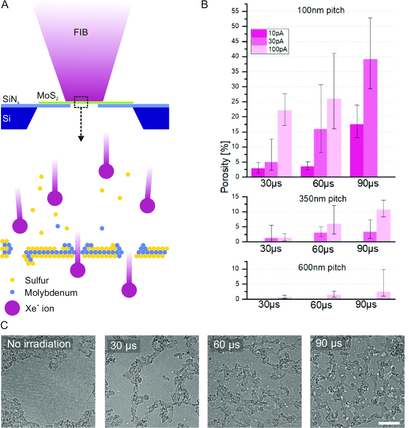
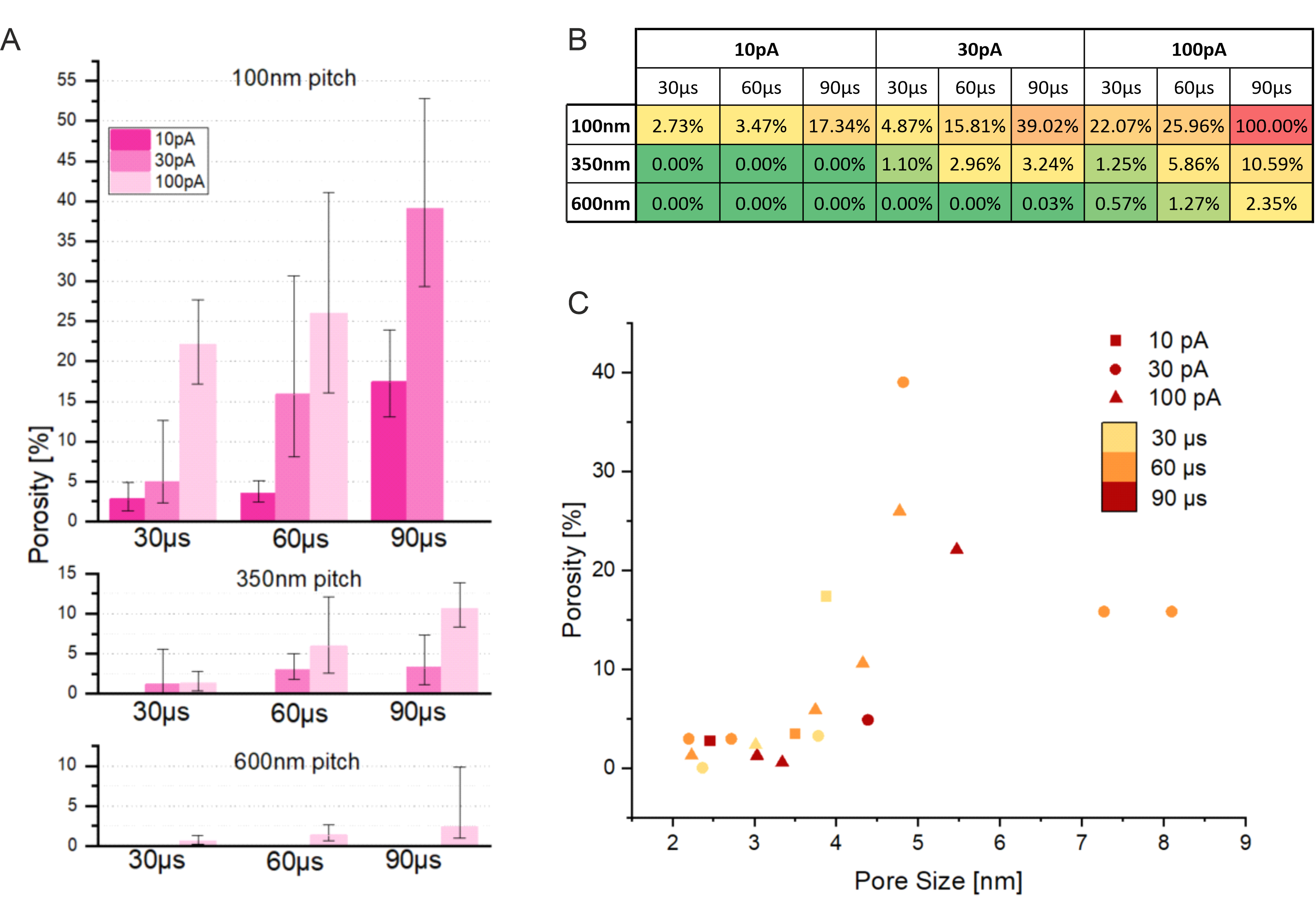
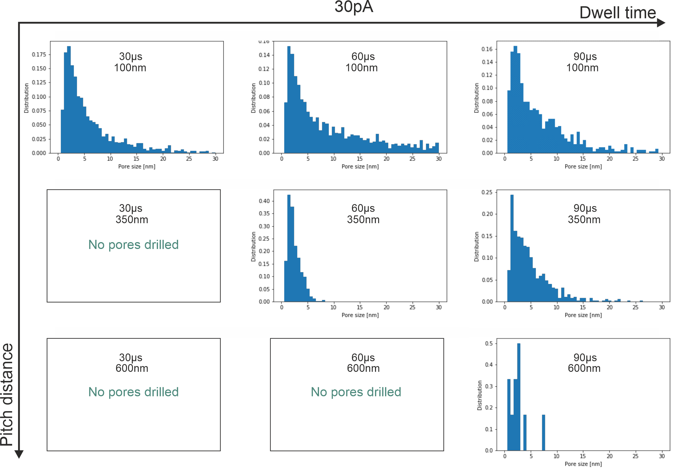
In our study, we used a Xe-ion plasma FIB system (see Methods section) as a nanopore fabrication platform. An MOCVD grown monolayer MoS2 (see Methods section) was transferred over a Si/SiN aperture and irradiated with Xe ions (Fig 1A) under varied ion beam parameters to investigate the nanopore fabrication performance, i.e. porosity and effective nanopore diameters (Fig. 1B,C). In all irradiation experiments, ion beam was kept at constant 30kV accelerating voltage with varying beam current of 10, 30, and 100pA, beam dwell time per pixel of 30, 60 and 90s and x/y distances between pixels (pitch distance) of 100, 350 and 600nm. Ion fluence was kept relatively low between and ion/cm2 to minimize beam damage and promote shower-like single ion collisions rather than wide-area milling. All irradiation experiments were performed with a single scan over the selected substrate area. Resulting membrane porosity was prescreened and quantified using Ilastik software package [29] (see Methods section) to obtain general insights into porosity and average pore size (Fig. S6A). Within the investigated FIB parameters, the nanopore-yielding parametric window is relatively narrow. Large pitch distances tend to yield no nanopores at lower beam currents, while membrane breakage was observed at 100pA, 90s, and 100nm pitch (Fig. S6B), corresponding to ion/cm2. The parameters and the effective diameters of the obtained nanopores are mapped in Fig. S6C. A more detailed parameter description of the used beam current, dwell time, and pitch distance is accessible in the supplementary information (Fig. S7-9). After investigating a range of nanopore-yielding parameters through high-resolution TEM (HRTEM) imaging, a second, in-depth nanopore analysis was performed on a membrane irradiated with 30kV, 30pA ion beam, 350nm in x/y pixel pitch distance and 60s dwell time per pixel (fluence of 6.77 ion/cm2). The porous membrane obtained with such a set of irradiation parameters yields pores of dimensions most relevant for applications such as desalination or biosensing (average of 1nm in Fig. S8).
2.2 Pore-edge detection
AC-STEM image analysis
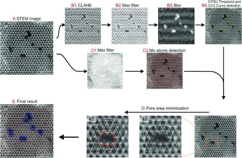
After prescreening the pore fabrication parameters with HRTEM imaging, MoS2 irradiated at the fluence of 6.77 ion/cm2 was selected for further, in-depth analysis with an expected average pore size of 1nm. AC-STEM was used to take detailed images of the irradiated film (see Methods for details). The resulting images were then used for further analysis and automated pore edge detection (Fig. 2). This task was divided into two parts: first, determining the positions of each atom species in the image, and second, determining the pore locations and extracting a polygon marking the pore edge. The latter also enabled us to study the distribution of fabricated pore shapes and the corresponding pore edge terminations.
STEM image processing and obtaining atom positions.
Obtaining the atomic positions in the lattice is critical to ensuring proper pore edge detection. A maximum filter with a constant fill is used with a lattice parameter roughly equal to approximately half the nearest-neighbour interatomic Mo-Mo distance , i.e., a parameter value of . This maximum filtered image (Fig. 2C is then processed to find the positions of the local maxima using the scikit-image [31] toolkit with a maximal separation of . The resulting maxima correspond to the positions of the individual Mo atoms. The positions of S atomic sites can then be obtained by repeating this procedure with half the maximum filter lattice parameter used before, followed by removal of the already detected Mo atom peaks from the population. This approach is robust, as it depends exclusively on the lattice unit cell distance; it could be further improved by taking into account the lattice symmetries of the given 2D material. We find that the positions of the sulphur atoms are less reliable due to a lower intensity relative to that of the molybdenum atoms, as well as the various contaminants or dirt present on the imaged surface. Consequently, the Mo atom sites are used as the reference for defining the pore locations.
Detecting the general pore locations.
Detecting pore locations using their general shape is a complex computer vision problem, which require the use of machine learning algorithms. In our case, due to the limited number of imaged pores and the complexity of the task, we opt for a classical image vision approach instead. We start with an approach similar to that described in Ref. [28]. We implement a contrast-limited adaptive histogram equalization (CLAHE) of the images to remove any variations in intensity due to variable illumination or dirt/contamination (Fig. 2B1). Unlike in the previous studies [28], our aim is not to obtain the exact pore edge at this stage, but to identify prospective pore locations for further analysis. We first use a maximum filter and then blur the resulting images in order to remove any smaller areas of a different contrast, which enables us to emphasize the nanopore locations (Fig. 2B2,B3). We use a maximum filter size, which is comparable to the Mo-Mo lattice distance in MoS2. We then combine thresholding using the Otsu method [32] with OpenCV contour find [30] to locate different pore contours (Fig. 2B4). The Otsu threshold algorithm does not involve any user defined parameters, leaving the expected lattice parameter used in the atom detection and maximum filtering as the only user defined parameter in the analysis. The end result is an approximation of the nanopore edge shape, which is then used with the Mo atom positions to detect the exact pore edge.
Pore edge optimisation.
By using the obtained nanopore contours (Fig. 2B4) and the positions of the Mo atoms (Fig. 2C2), we are able to identify nanopore edges with reasonably high precision without freely adjustable parameters. For each detected nanopore contour curve, we consider a group of Mo atoms consisting of any atoms within two typical Mo-Mo distances from the contour (Fig. 2D). First, a convex hull is constructed from this group of atom positions, and then from it a polygon with edges between the sites corresponding to the distance between the nearest Mo-Mo neighbours () is composed. This polygon (blue in Fig. 2 4A) is then optimized using a custom algorithm (Supplemental Sec. 5.1) so that its surface area is minimized, while maintaining nearest-neighbour distances on the triangular Mo sub-lattice. The algorithm seeks out any local changes in the polygon edges that reduce the total polygon surface area by removing or adding Mo sites. In case the algorithm is unable to converge to a valid pore shape, the group of atoms used for the original convex hull is expanded toward any nearby neighbouring groups of atoms, which did not yield a valid pore shape either. If no such group of atoms is found, the pore is then rejected from the statistic. This procedure automatically rejects all pores located close to the STEM image edge, such that parts of the missing edges are not visible.
Identifying pore edges
Having obtained the coordinates of the Mo atoms forming a polygon outlining each nanopore, we can identify the composition of the pore interior edge and thus attempt to estimate its permeation properties on theoretical grounds. Depending on whether the edge composition is dominated by Mo and S atoms (carrying positive and negative partial atomic charges, respectively), a rich variety of tunable permeation properties is expected [33, 34], as also discussed in greater detail later in the text. In this sense, nanopores in single-layer MoS2 are in fundamental contrast from those graphene-based, where pore edge termination appears to be close to neutral [35] without functionalization. In addition, unbiased graphene membranes carry no overall surface charge density that could electrostatically boost osmotic currents through small pores. Within the scope of this work, we assume that the in-solvent MoS2 pore structures are close to those imaged post-fabrication. Of course, further in-solvent functionalization (e.g., with hydroxyl groups) is possible to for example control hydrophilicity of the pore interior. More generally, the character of pore edge chemistry directly influences the electrostatic interactions inside the pore and thus further modifies the permeation properties [36, 37, 33, 34, 38]. The first step in predicting the properties of porous 2D membranes is thus to identify the pore edge composition of the manufactured pores.
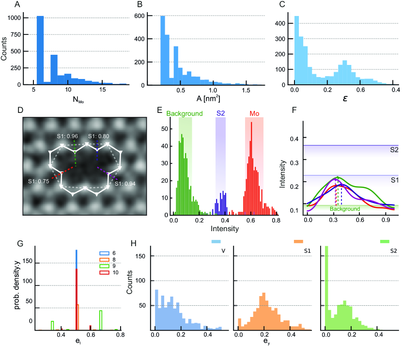
Starting with a polygon marking the Mo sites sites at the nanopore edge, we determine the positions of the sulphur sites in the lattice (Fig. 3). This subsequently enables us to identify the complete atomic pattern marking the edge of the nanopore. Such a pattern will have the form of Mo--Mo--Mo--…with either a Sulphur site that is not directly exposed to the nanopore (it is interior to the lattice, marked as I) or an edge-exposed site. Exposed sites can be a double sulphur (marked as S2), single sulphur (S1) or empty (V). Intensities of atoms are known to scale with the atomic number [39] so we proceed by comparing the intensities at the edge atomic sites with reference values. As shown in Fig. 3, reference atom intensities are obtained from full STEM images, which usually feature multiple nanopores. The same peak identification algorithm as described in Fig. 2C is used to detect S2 and the background levels, except the lattice parameter is appropriately reduced and an inverse of the image used, respectively. The population of each sites is then obtained by removing each sub-population from the full statistic. The statistics for S2 sites is of lower quality, as it is harder to identify positions of S2 in the lattice compared to the more intense Mo positions or similar S1. The S1 intensity value is determined as the average of the background intensity (V) and S2 intensity values. Based on the obtained distributions of intensity values for different atoms, we proceed to identify each S site at the pore edge. For each sulphur site at the pore edge we perform slicing of the intensity perpendicular to the sites corresponding to the Mo-Mo polygon edge (Fig. 3b), starting from the position of the dark spot and towards the nanopore interior. We calculate the mean intensity values and the corresponding standard deviations for each intensity group corresponding to four possible atom types (V, S1, S2, Mo). If a site does not have a prominent well-defined peak or is buried under the noise level defined by the background intensity distribution (V in Fig. 3a), it is identified as invalid (marked X). We find that invalid sites occur when either the pore edge was improperly recognized, or when the pore is contaminated. Full details of the algorithm are provided in the supplement. Assuming that the site intensity is obtained from the four independent normal probability distributions, we can extract the probability that a site on the edge corresponds to any of the three possible site types (V, S1, S2).
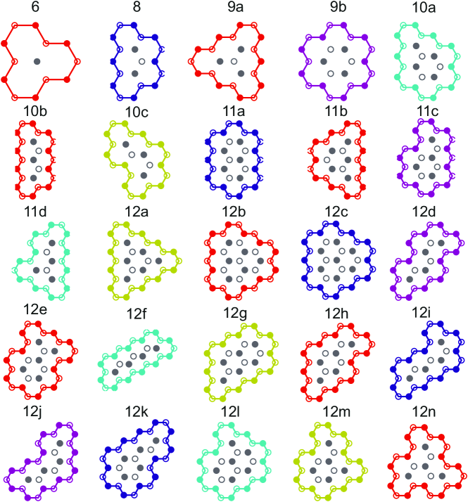
We are now able to compare the different parameters obtained with analysis software from STEM images of irradiated samples. Fig. 3a,b,c shows histograms on the full statistic of nanopores identified using our algorithm. The distribution of the number of molybdenum atoms in the nanopore edge indicates that there are preferential shapes for the pores involving Mo atoms, along with the corresponding nanopore areas as seen for the histogram of pore area values . The elongation of different pores is represented by the eccentricity with and being the minor and major axii of the nanopore, respectively, as estimated from the dimensions of the corresponding minimum and maximum bounding rectangles. This approach yields a value of for perfectly circular nanopores, and for a pore of infinite length in one dimension. In our case, there is a population of nanopores of circular shapes (), and those with a defined elongation of about an , matching the most populous elongated pore shapes (marked as 8 in Supplemental Fig. S10).
Our analysis also allows investigating the sulphur content of the nanopore edge. We define as the fraction of -sites for each pore edge, such that the fraction of interior (non-edge-exposed) sites is and the fraction of V, S1, S2 sites, as . Here is the number of interior sites for a given pore. For arbitrary pore shapes, as shown in Fig. 3g, half of the sulphur sites are on average interior to the lattice, with another half exposed at the pore edge. A small sub-population of nanopores (linked to the shapes associated with , for instance) has longer zig-zag edge segments. Depending on the orientation of the lattice, this group produces two types of pores with different fractions of edge-exposed S-sites, as shown in Fig. 3h. We note that there appears to be a slightly higher probability of finding S1 sites at these edge-exposed sites, compared to S2 or V sites. Overall, the dominance of Mo-terminated edges is due to the relatively high knock-on energy threshold needed for the incident beam to displace the Mo atom [40] compared to that required for S atoms. Additionally, this threshold is further lowered for the edge atoms due to reduced coordination, thus making edge sulphurs (especially the single-sulphur sites) fundamentally less stable during irradiation [40] as compared to molybdenum.
Edge shape detection at the atomic resolution
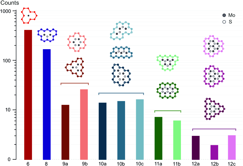
Once the polygon shapes marking the Mo and S atoms at the nanopore edge are known, we can identify the likely nanopore shapes in the analysed images. Combinatorially, when the amount of Mo atoms lining the edge becomes large (in our case, , a near-exponential increase in the number of the pore structure possibilities is expected [41]. Taking into account that our analysis indicates a small probability of generating pores past that size, we limit our analysis of shapes up to . This constitutes a maximum number of 3 (7) removed Mo (S) atoms from the lattice. We also limit ourselves to not considering the removal of pore edge exposed atoms, including them in our analysis of the site occupancy in Fig. 3h. To classify our pores (See Supplemental Fig. S10 for a complete list of pores included in our classification), we first remove from the statistic any nanopores which are severely deformed or contaminated (i.e. any edge S site is identified as invalid - X). Then we match the unique pattern of interior and exterior edge S atom sites between an unknown pore and the database of known nanopore shapes. In most cases misidentified shapes are due to the underlying atomic lattice being deformed, causing shapes which do not conform to normal lattice parameters. In our case, we note that about 1% such invalid pores are identified for , 6% for , 13% for , 27% for and 34% for . If there are multiple shapes with the same pattern (in our case, for there are only two such shapes), we use the hu-moment based image recognition to determine the most probable match. Fig. 4 show the histogram of identified pore shapes up to N=12. Herein, all pores with invalid geometries, or with unidentifiable (classified as X) edge sites, have been removed from the presented statistic. We see that certain pore types are considerably more probable, e.g., the shape identified as 9b with more Mo atoms exposed to the pore interior is more probable than 9a, which has more sulphur sites exposed to the pore edge. Larger pores, with , appear to be overall improbable in the Xe irradiated samples presented here. We find that the major source of error for the algorithm stems from the uncertainty in identifying what is an actual Mo atom in the lattice, and differentiating the atom from adatoms and contaminants. Most cases of irregular shapes identified with the algorithm, which are rejected from the analysis in Fig. 4 as they do not match a known shape, come from anomalous lattice atom positions. Such cases result from STEM imaging artifacts or unexpected adatoms or pore contamination. This can be improved upon in the future by using a better algorithm to detect atoms which takes into account the symmetry of the atomic lattice.
Permeation property prediction
Once the individual pore structures have been obtained, their properties can be estimated. Here we consider ion and water permeation through the pores comprising the statistics in Fig. 4 and shown in Fig. 5A, as obtained from all-atom molecular dynamics (MD) simulations described in detail in Section 4. To investigate ion flow driven by a constant electric field, MD simulations were set up similarly to our previous work on the transport mechanisms in subnanoporous 2D materials [18, 19, 42]. For pressure-driven water flow, external hydraulic pressure was induced in the form of a constant force acting upon a solid piston. Sketches of systems driven by electric field and hydraulic pressure are shown in Fig. 5B.
As summarized in Fig. 5B, most pores in Fig. 4 are ion-impermeable under a realistic electrostatic bias. The obvious factors here are the pore size (the number of removed atomic sites) and the pore eccentricity, i.e., sufficiently elongated pores preclude ionic permeability through high steric repulsion regardless of the pore length along the larger dimension. Other mechanisms consistent with earlier observations [19, 42] are more subtle and arise from the fact that Mo and S2 carry partial positive and negative charges, respectively. Consider the fact that all ionic currents reported in Fig. 5B were contributed by anions (Cl-). This observation likely owes to the electric field distribution near bulk MoS2 monolayer surface, which is a finitely-spaced S--Mo++-S- sandwich from the electrostatic standpoint. This electrostatic configuration appears to be overall repulsive to cations, also partly responsible for interlayer adhesion in multilayer MoS2. Given this broad selectivity, anion transport is further boosted in pores featuring Mo+-lined edges, despite the net zero charge of both the pore and the host membrane. Consider for example the 9b’ and 12a pores, which are structural conjugates (geometrically identical, except the S2 and Mo atomic sites are swapped): while 9b’ lined with Mo atoms features sizeable ionic conductance, 12a is impermeable to anions. For the same reason, 12b, which is primarily lined with Mo atoms, has a significantly larger conductance than its structural conjugate 12c, except that now both 12b and 12c are ion-permeable due to their considerably larger size. Simulated pressure-induced water transport is shown to be rather low, being of order , as shown in the table in Fig. 5B. Although such a low permeability renders the pore sizes considered here likely unfeasible for broad nanofluidic applications [12], given the overall high levels of ion rejection, they remain promising for desalination [9, 10] and possibly gas filtration systems [11].

The simulated properties of the individual pores identified here enable us to make several observations regarding mechanosensing [18, 19, 20], which is another emerging area of application for solid 2D nanopores. Some of the structures identified here have ion transport properties, which can be modulated by the application of mechanical strain to the membrane hosting the pore. Fig. 5C shows ionic currents under an electrical bias as a function of isotropic membrane strain. Observing this effect in experiments introduces a potential challenge. Currently, applying hydrostatic pressure in the direction perpendicular to the membrane appears to be the only realistic way to induce dilation of 2D nanopores [43]. Consequently, the resulting streaming flow may in principle compete with the effect of pore dilation on the ionic transport. Furthermore, depending on the relative directions of pressure and the external electrostatic bias, the two effects could in fact oppose each other. Although the data in Fig. 5B suggests overall low streaming couplings that at the most contribute currents of order 0.8 pA for pressures of order 20 bar, the coexistence of these effects must be taken into account when probing mechanosensitivity with the use of hydrostatically pressurized nanofluidic cells.
Once the individual pores have been quantified, for a given membrane hosting a large population of pores described in Fig. 4, a predictive estimate of the membrane-wide permeation properties becomes possible. In the simplest case, assuming that the pores are spaced sufficiently sparsely so as not to affect each other’s properties, these estimates are straightforward. For example, for a total of pores possessing a set of ionic conductance values and corresponding selectivity values , the membrane-wide conductance and selectivity are and , respectively. Similarly, the mechanosensitivity (as defined earlier [18]) for the entire membrane is , where are the individual mechanosensitivity values of the constituent pores. These estimates underscore the importance of obtaining accurate statistics of both the pore structures and the corresponding structure histograms. It is important to keep in mind that large numbers of impermeable pores in a given population have virtually no effect on permeability, while a relatively small number of highly permeable non-selective pores can readily "smear" the desirable membrane-wide properties. Overall, judicious use of the estimates discussed above may result in a promising fabrication parameter tuning tool that enables achieving desirable membrane-wide permeation properties and reduces the number of trial-and-error permeation measurements.
3 Conclusion
We have demonstrated the viability of Xe-ion irradiation as a large-scale nanopore fabrication tool. The presented irradiation protocol enables designing membranes with tunable porosity and pore dimension tuning, along with spatial uniformity across large-area substrates. Fabricated nanoporous membranes were characterized using STEM imaging and observed nanopore geometries were analyzed through a pore-edge detection script which depends only on one user defined parameter, the lattice constant of the 2D material in question. Our pore detection algorithm allows resolving individual pore structures and combining it into a membrane-wide statistical analysis of the entire pore population. We then demonstrated that the obtained structural and statistical data can be readily passed on to computational and analytical tools to predict the permeation properties at both individual pore and membrane-wide scales. As an example, membranes featuring angstrom-scale pores were investigated in terms of their emerging fluid and ion flow properties through extensive all-atom MD simulations.
High-quality structural and statistical descriptions of as-fabricated porous membranes are key to predicting the corresponding membrane-wide permeation properties. It is worth noting that as presented here and as would be the case with any image-based analysis, there fundamentally exists a degree of uncertainty in the resulting data. This arises from both uncertainty of the pore edge Sulphur sites being vacant, but also in the specifics of identifying the exact pore shapes. Therefore, the subsequent use of highly accurate (assuming proper parameterization), but computationally intensive methods (e.g., MD) to convert the structural and statistical data into permeation property predictions may be excessive. Instead, semi-analytical estimates of the permeation properties of individual nanopores and entire membranes could prove both reasonably accurate and highly computationally efficient. Although such estimation methods are challenging to implement, individual steps are already being taken towards for example rapid screening of nanopores [44] or a detailed analytical formulation of how water molecules behave near nanopores [45]. We believe that further improvements in the on-the-fly conversion of the structural and statistical data into an accurate physics-based property estimates should yield software tools that enable a true function-by-design approach to fabrication for applications such as mechanosensing, osmotic power generation, desalination, and filtration.
4 Methods
Substrate fabrication MoS2 was synthesised on c-cut sapphire wafer in metalorganic chemical vapor deposition (MOCVD) tube-furnace using large-scale growth methodology [46, 47]. As-grown material was transferred onto TEM SiN holey grids (Norcada) via polymer-assisted transfer method [46]. Before and after FIB processing suspended MoS2 membranes were washed in acetone and soft-baked at 150∘C for 2h to minimize airborne hydrocarbon contamination and beam-induced deposition.
Focused Ion Beam Irradiation Ion irradiation was performed at ThermoFischer Helios G4 PFIB DualBeam with Xenon Plasma FIB column. All FIB irradiation experiments were performed at constant 30kV with varying beam current, dwell time and pitch distance. Irradiated area was 200x200m, centered at the substrate grid/membrane location.
HRTEM image analysis and machine learning Transmission Electron Microscopy imaging was done on the ThermoFischer Talos F200S at 80kV accelerating voltage. Obtained high resolution images of nanoporous films were then cropped and bandpass-filtered. Subsequent machine-learning pore segmentation was performed in Ilastik and further processed and analyzed with Fiji ImageJ2. Due to the complexity of pore-detection and insufficient resolution, the more detailed analysis was performed with AC-STEM micrographs and custom-made analysis script described in the main text.
STEM imaging Scanning transmission electron microscopy imaging was conducted using an aberration-corrected (with double spherical corrector) FEI Titan Themis TEM 60 - 300 kV, equipped with Schottky X-FEG electron source and a monochromator to reduce the effect of chromatic aberrations. To avoid the electron-beam induced knock-on damage, a low acceleration voltage (80 kV) was used for the imaging [48]. The electron probe current, C2 aperture size, and a beam convergence angle was 25pA, 50m, and 21.2 mrad, respectively. Images were acquired with a Velox software (ThermoFisher Scientific) using 185 mm camera length which corresponds to an angular range (49.5 - 198 mrad) in a HAADF detector. To minimize the sample drift, a serial imaging was performed using 512 × 512 pixels with 8 s dwell time. Images were aligned and processed using the double-Gaussian filtering method in ImageJ.
MD simulations The all-atom MoS2 model was set up according to recently published work [49], implemented within the OPLS-AA framework [50, 51]. The atomic charges of Mo and S sites at the zigzag edges of the pores were set to of their bulk counterparts (for bulk charges, see Ref. [49]), corresponding to and , respectively. Such an assignment guarantees overall electrostatic neutrality of the zigzag edge and thus all pore structures considered in this work regardless of their geometry. Explicitly simulated water molecules were described according to the TIP4P model [52] while ions were described according to default OPLS-AA [50, 51].
The simulations were performed using the GPU-accelerated Gromacs package [53, 54] (version 2021.4). Ion and water transport through the pores was simulated in the presence of water-dissociated 1M KCl. The simulation cell sizes were approximately nm3 and nm3 for the ion and water flow simulations, respectively. In all simulations, the atoms at the perimeter of the porous membrane were harmonically restrained against displacement along X, Y, and Z ( N/m), while the piston membrane in the pressure-driven simulations was free to move. The constant vertical force acting upon the piston was , where (in the range 10-50 bar) is the desired pressure, nm2 is the in-plane cross-sectional area of the simulation cell. In the ion flow simulations, the external electric field (of order 0.02 V/nm) was , where V is the potential difference consistent with voltages typically applied in experiments and nm is the height of the simulation cell, respectively. Periodic boundary conditions were applied in the -directions. After initial equilibration at constant = 1 atm and = 300 K, constant-volume production simulations were performed at = 300 K for at least 0.5 to ensure reasonable permeation statistics.
Authors Contribution M.M. synthesized MoS2, developed the irradiation process and performed materials characterization and imaging; S.M. wrote pore-edge analysis script; M.Tripathi performed AC-STEM imaging; M.Thakur and M.L did material transfer; A.S. designed and performed MD simulations. M.M., S.M., and A.S. analyzed the data, developed the key concepts, and wrote the manuscript with inputs from all authors. A.R. supervised the project. All authors discussed the results and commented on the manuscript.
Acknowledgments This work was in part financially supported by a Swiss National Science Foundation (SNSF) support through 200021192037 and the CCMX Materials Challenge grant “Large area growth of 2D materials for device integration”. A.S. gratefully acknowledges support from the Materials Genome Initiative.
Disclaimer Commercial equipment, instruments, or materials are identified only in order to adequately specify certain procedures. In no case does such identification imply recommendation or endorsement by the National Institute of Standards and Technology, nor does it imply that the products identified are necessarily the best available for the purpose.
5 Supplementary information


5.1 Pore shape optimisation
To obtain the exact edge of a nanopore we start with a group of atoms each with coordinates centered around a suspected nanopore location. For each pore we proceed as follows.
First, a convex hull polygon is generated which by its definition envelops all the points in the group. For each edge pair of atoms in this polygon, we find the shortest path between them on a matrix of nearest neighbour atoms (). A new polygon with points is then generated as a union of all shortest paths between the original convex hull polygon edge points. The resulting polygon approximates the original convex hull but with edge/side lengths corresponding to the individual Mo-Mo atom distances.
Secondly, we repeat the following procedure over the polygon, generating a new polygon which then replaces the original polygon until the algorithm converges to the new polygon matching the old one ( = ).
For each atom in the polygon , taking into account that the polymer is cyclic (), test for one of the following cases:
-
1.
Remove dangling atom: If - - form a dangling bond (), then remove from the polygon to form if the resulting polygon would have a smaller area than .
-
2.
Remove extra atom: If and are nearest neighbours (), then remove from the polygon to form if the resulting polygon would have a smaller area than .
-
3.
Exchange atom: If there is an such that it is a nearest neighbour of both and (), then replace with to form a new if the resulting polygon would have a smaller area than .
-
4.
Add new atom: If there is an such that it is a nearest neighbour of both and (), then add between and to form a new if the resulting polygon would have a smaller area than .
If the optimized pore edge has been found and the algorithm is stopped, if not make the new and repeat the previous procedure.
5.2 Pore edge atom detection
For each possible Sulphur site exposed at the nanopore edge, a slice is made by using a spline interpolation of the STEM image between two points perpendicular to the line connecting the two closest nanopore edge Molybdenum atoms (gray dashed lines in Fig. 3D). The starting point for the slice is located at a distance of two Mo-S-Mo triangle heights on the opposite side of the expected Sulphur atom position in respect to the Mo-Mo line. The end point of the slice is located at away from the expected triangle site. Note that the intensity values plotted are normalized to 1 for the highest intensity pixel in the whole image, and 0 for the lowest intensity pixel.
The intensity along the slice (colored dashed lines in Fig. 3D) is then evaluated to determine the probability of finding a certain "atom type" at that side: a vacancy (V), double sulphurs (2S), single sulphur (S), or an invalid site (X).
A site is declared invalid (X) if the last or fist point in the slice curve is also the maximum of the curve, unless the curve is constantly below the mid value between the expected sulphur and vacancy intensity level. In addition, if the values at the beginning or end of the slice are at the level expected for S1 or higher, they are rejected. These tests ensure that an invalid pore polygon shape is not used for further recognition. Also, each Mo polygon obtained from the pore shape optimisation algorithm can yield two possible Mo-S-Mo- polygons. In order to determine the one correct polygon out of the two possibilities that match the proper crystal lattice arrangement, we perform two edge detection runs for each of the two possible polygons and reject the one with the greatest number of invalid edge sites.
The final criteria for a valid pore edge detection is the value of the most prominent peak found in the contour, as obtained using the find peaks function of the Scipy signal processing library. The minimum peak height and prominence of 0.05 and 0.01 are used, respectively. If there is no peak found or if the most prominent peak doesn’t have at least twice the prominence of all the detected peaks combined, the corresponding site is declared a vacancy (V).
If a site has not been identified as a vacancy or as invalid, the most prominent peak value is compared to the average intensities of Mo and S2 obtained from the histograms of the atom sites in the entire STEM image studied (Fig. 3E). From this data, we obtain the probability that the site corresponds to a certain atom type, as described in the main text.
References
- Jiang et al. [2019] Jie Jiang, Tao Xu, Junpeng Lu, Litao Sun, and Zhenhua Ni. Defect Engineering in 2D Materials: Precise Manipulation and Improved Functionalities. Research, 2019:1–14, 12 2019. ISSN 26395274. doi:10.34133/2019/4641739.
- Ahn [2020] Ethan C. Ahn. 2D materials for spintronic devices. npj 2D Materials and Applications 2020 4:1, 4(1):1–14, 6 2020. ISSN 2397-7132. doi:10.1038/s41699-020-0152-0.
- Zhang et al. [2021] Miao Zhang, Martina Lihter, Tzu-Heng Chen, Michal Macha, Archith Rayabharam, Karla Banjac, Yanfei Zhao, Zhenyu Wang, Jing Zhang, Jean Comtet, Narayana R. Aluru, Magalí Lingenfelder, Andras Kis, and Aleksandra Radenovic. Super-resolved Optical Mapping of Reactive Sulfur-Vacancies in Two-Dimensional Transition Metal Dichalcogenides. ACS Nano, 15(4):7168–7178, 4 2021. ISSN 1936-0851. doi:10.1021/acsnano.1c00373.
- Caldwell et al. [2019] Joshua D. Caldwell, Igor Aharonovich, Guillaume Cassabois, James H. Edgar, Bernard Gil, and D. N. Basov. Photonics with hexagonal boron nitride. Nature Reviews Materials 2019 4:8, 4(8):552–567, 7 2019. ISSN 2058-8437. doi:10.1038/s41578-019-0124-1.
- Glushkov et al. [2021] Evgenii Glushkov, Michal Macha, Esther Rath, Vytautas Navikas, Nathan Ronceray, Cheol Yeon Cheon, Ahmed Aqeel, Ahmet Avsar, Kenji Watanabe, Takashi Taniguchi, Ivan Shorubalko, Andras Kis, Georg Fantner, and Aleksandra Radenovic. Engineering optically active defects in hexagonal boron nitride using focused ion beam and water. 7 2021. URL https://arxiv.org/abs/2107.02254v1.
- Tuller and Bishop [2011] Harry L. Tuller and Sean R. Bishop. Point Defects in Oxides: Tailoring Materials Through Defect Engineering. http://dx.doi.org/10.1146/annurev-matsci-062910-100442, 41:369–398, 7 2011. ISSN 15317331. doi:10.1146/ANNUREV-MATSCI-062910-100442.
- Zhong et al. [2022] Kai Zhong, Rupeng Bu, Fangbao Jiao, Guangrui Liu, and Chaoyang Zhang. Toward the defect engineering of energetic materials: A review of the effect of crystal defects on the sensitivity. Chemical Engineering Journal, 429:132310, 2 2022. ISSN 1385-8947. doi:10.1016/J.CEJ.2021.132310.
- Lin et al. [2016] Zhong Lin, Bruno R. Carvalho, Ethan Kahn, Ruitao Lv, Rahul Rao, Humberto Terrones, Marcos A. Pimenta, and Mauricio Terrones. Defect engineering of two-dimensional transition metal dichalcogenides. 2D Materials, 3(2):022002, 4 2016. ISSN 2053-1583. doi:10.1088/2053-1583/3/2/022002.
- Ali et al. [2018] Aamer Ali, Ramato Ashu Tufa, Francesca Macedonio, Efrem Curcio, and Enrico Drioli. Membrane technology in renewable-energy-driven desalination. Renewable and Sustainable Energy Reviews, 81(July 2017):1–21, 2018. ISSN 18790690. doi:10.1016/j.rser.2017.07.047.
- Thiruraman et al. [2020a] Jothi Priyanka Thiruraman, Paul Masih Das, and Marija Drndić. Ions and Water Dancing through Atom-Scale Holes: A Perspective toward “Size Zero”. ACS Nano, 2020a. ISSN 1936086X. doi:10.1021/ACSNANO.0C01625.
- Thiruraman et al. [2020b] Jothi Priyanka Thiruraman, Sidra Abbas Dar, Paul Masih Das, Nasim Hassani, Mehdi Neek-Amal, Ashok Keerthi, Marija Drndić, and Boya Radha. Gas flow through atomic-scale apertures. Science Advances, 6(51), 12 2020b. ISSN 2375-2548. doi:10.1126/sciadv.abc7927.
- Macha et al. [2019] Michal Macha, Sanjin Marion, Vishal V.R. Nandigana, and Aleksandra Radenovic. 2D materials as an emerging platform for nanopore-based power generation. Nature Reviews Materials 2019 4:9, 4(9):588–605, 7 2019. ISSN 2058-8437. doi:10.1038/s41578-019-0126-z.
- Xue et al. [2020] Liang Xue, Hirohito Yamazaki, Ren Ren, Meni Wanunu, Aleksandar P. Ivanov, and Joshua B. Edel. Solid-state nanopore sensors. Nature Reviews Materials 2020 5:12, 5(12):931–951, 9 2020. ISSN 2058-8437. doi:10.1038/s41578-020-0229-6.
- Drndić [2014] Marija Drndić. Sequencing with graphene pores. Nature Nanotechnology 2014 9:10, 9(10):743–743, 10 2014. ISSN 1748-3395. doi:10.1038/nnano.2014.232.
- Heerema and Dekker [2016] Stephanie J. Heerema and Cees Dekker. Graphene nanodevices for DNA sequencing, 2016. ISSN 17483395.
- Merchant et al. [2010] Christopher A. Merchant, Ken Healy, Meni Wanunu, Vishva Ray, Neil Peterman, John Bartel, Michael D. Fischbein, Kimberly Venta, Zhengtang Luo, A. T.Charlie Johnson, and Marija Drndić. DNA translocation through graphene nanopores. Nano Letters, 2010. ISSN 15306984. doi:10.1021/nl101046t.
- Feng et al. [2015] Jiandong Feng, Ke Liu, Roman D. Bulushev, Sergey Khlybov, Dumitru Dumcenco, Andras Kis, and Aleksandra Radenovic. Identification of single nucleotides in MoS2 nanopores. Nature Nanotechnology, 2015. ISSN 1748-3387. doi:10.1038/nnano.2015.219.
- Fang et al. [2018a] A. Fang, K. Kroenlein, D. Riccardi, and A. Smolyanitsky. Highly mechanosensitive ion channels from graphene-embedded crown ethers. Nature Materials 2018 18:1, 18(1):76–81, 11 2018a. ISSN 1476-4660. doi:10.1038/s41563-018-0220-4.
- Fang et al. [2019] A. Fang, K. Kroenlein, and A. Smolyanitsky. Mechanosensitive Ion Permeation across Subnanoporous MoS <sub>2</sub> Monolayers. The Journal of Physical Chemistry C, 123(6):3588–3593, 2 2019. ISSN 1932-7447. doi:10.1021/acs.jpcc.8b11224.
- Marion and Radenovic [2020] Sanjin Marion and Aleksandra Radenovic. Towards artificial mechanosensing. Nature Materials 2020 19:10, 19(10):1043–1044, 9 2020. ISSN 1476-4660. doi:10.1038/s41563-020-00811-5.
- Fang et al. [2018b] Mingxu Fang, Fang Wang, Yemei Han, Yulin Feng, Tianling Ren, Yue Li, Dengxuan Tang, Zhitang Song, Kailiang Zhang, M Fang, F Wang, Y Han, Y Feng, Y Li, D Tang, K Zhang, and T Ren. Controlled Growth of Bilayer-MoS2 Films and MoS2-Based Field-Effect Transistor (FET) Performance Optimization. Advanced Electronic Materials, 4(4):1700524, 4 2018b. ISSN 2199-160X. doi:10.1002/AELM.201700524.
- Vlassiouk et al. [2008] Ivan Vlassiouk, Sergei Smirnov, and Zuzanna Siwyt. Ionic selectivity of single nanochannels. Nano Letters, 2008. ISSN 15306984. doi:10.1021/nl800949k.
- Heiranian et al. [2015] Mohammad Heiranian, Amir Barati Farimani, and Narayana R. Aluru. Water desalination with a single-layer MoS 2 nanopore. Nature Communications, 6:1–6, 2015. ISSN 20411723. doi:10.1038/ncomms9616.
- Danda and Drndić [2019] Gopinath Danda and Marija Drndić. Two-dimensional nanopores and nanoporous membranes for ion and molecule transport. Current Opinion in Biotechnology, 55:124–133, 2 2019. ISSN 0958-1669. doi:10.1016/J.COPBIO.2018.09.002.
- Fried et al. [2021] Jasper P. Fried, Jacob L. Swett, Binoy Paulose Nadappuram, Jan A. Mol, Joshua B. Edel, Aleksandar P. Ivanov, and James R. Yates. In situ solid-state nanopore fabrication. Chemical Society Reviews, 50(8):4974–4992, 4 2021. ISSN 1460-4744. doi:10.1039/D0CS00924E.
- Graf et al. [2019] Michael Graf, Martina Lihter, Mukeshchand Thakur, Vasileia Georgiou, Juraj Topolancik, B. Robert Ilic, Ke Liu, Jiandong Feng, Yann Astier, and Aleksandra Radenovic. Fabrication and practical applications of molybdenum disulfide nanopores. Nature Protocols, 14(4):1130–1168, 4 2019. ISSN 17502799. doi:10.1038/S41596-019-0131-0.
- Thiruraman et al. [2018] Jothi Priyanka Thiruraman, Kazunori Fujisawa, Gopinath Danda, Paul Masih Das, Tianyi Zhang, Adam Bolotsky, Néstor Perea-López, Adrien Nicolaï, Patrick Senet, Mauricio Terrones, and Marija Drndić. Angstrom-Size Defect Creation and Ionic Transport through Pores in Single-Layer MoS2. Nano Letters, 2018. ISSN 15306992. doi:10.1021/acs.nanolett.7b04526.
- Chen et al. [2021] Joshua Chen, Adrian Balan, Paul Masih Das, Jothi Priyanka Thiruraman, and Marija Drndić. Computer vision AC-STEM automated image analysis for 2D nanopore applications. Ultramicroscopy, 231:113249, 12 2021. ISSN 0304-3991. doi:10.1016/J.ULTRAMIC.2021.113249.
- Berg et al. [2019] Stuart Berg, Dominik Kutra, Thorben Kroeger, Christoph N. Straehle, Bernhard X. Kausler, Carsten Haubold, Martin Schiegg, Janez Ales, Thorsten Beier, Markus Rudy, Kemal Eren, Jaime I. Cervantes, Buote Xu, Fynn Beuttenmueller, Adrian Wolny, Chong Zhang, Ullrich Koethe, Fred A. Hamprecht, and Anna Kreshuk. ilastik: interactive machine learning for (bio)image analysis. Nature Methods 2019 16:12, 16(12):1226–1232, 9 2019. ISSN 1548-7105. doi:10.1038/s41592-019-0582-9.
- Bradski [2000] G. Bradski. The OpenCV Library. Dr. Dobb’s Journal of Software Tools, 2000.
- der Walt et al. [2014] Stefan der Walt, Johannes L Schönberger, Juan Nunez-Iglesias, François Boulogne, Joshua D Warner, Neil Yager, Emmanuelle Gouillart, and Tony Yu. scikit-image: image processing in Python. PeerJ, 2:e453, 2014.
- Otsu [1979] Nobuyuki Otsu. THRESHOLD SELECTION METHOD FROM GRAY-LEVEL HISTOGRAMS. IEEE Trans Syst Man Cybern, SMC-9(1):62–66, 1979. ISSN 00189472. doi:10.1109/TSMC.1979.4310076.
- Lee et al. [2014] J. Lee, Z. Yang, W. Zhou, S. J. Pennycook, S. T. Pantelides, and M. F. Chisholm. Stabilization of graphene nanopore. Proceedings of the National Academy of Sciences, 2014. ISSN 0027-8424. doi:10.1073/pnas.1400767111.
- Yang et al. [2017] Tieshan Yang, Han Lin, Xiaorui Zheng, Kian Ping Loh, and Baohua Jia. Tailoring pores in graphene-based materials: From generation to applications, 2017. ISSN 20507496.
- Rollings et al. [2016] Ryan C. Rollings, Aaron T. Kuan, and Jene A. Golovchenko. Ion selectivity of graphene nanopores. Nature Communications, 7:1–7, 2016. ISSN 20411723. doi:10.1038/ncomms11408.
- Surwade et al. [2015] Sumedh P. Surwade, Sergei N. Smirnov, Ivan V. Vlassiouk, Raymond R. Unocic, Gabriel M. Veith, Sheng Dai, and Shannon M. Mahurin. Water desalination using nanoporous single-layer graphene. Nature Nanotechnology, 10(5):459–464, 2015. ISSN 17483395. doi:10.1038/nnano.2015.37.
- Walker et al. [2017] Michael I. Walker, Krystian Ubych, Vivek Saraswat, Edward A. Chalklen, Philipp Braeuninger-Weimer, Sabina Caneva, Robert S. Weatherup, Stephan Hofmann, and Ulrich F. Keyser. Extrinsic Cation Selectivity of 2D Membranes. ACS Nano, 11(2):1340–1346, 2017. ISSN 1936086X. doi:10.1021/acsnano.6b06034.
- Liu et al. [2018] Qiuwen Liu, Cheng Chen, Man Du, Yawei Wu, Chunjin Ren, Kaining Ding, Mingxia Song, and Caijin Huang. Porous Hexagonal Boron Nitride Sheets: Effect of Hydroxyl and Secondary Amino Groups on Photocatalytic Hydrogen Evolution. ACS Applied Nano Materials, 1(9):4566–4575, 9 2018. ISSN 2574-0970. doi:10.1021/acsanm.8b00867.
- Krivanek et al. [2010] Ondrej L. Krivanek, Matthew F. Chisholm, Valeria Nicolosi, Timothy J. Pennycook, George J. Corbin, Niklas Dellby, Matthew F. Murfitt, Christopher S. Own, Zoltan S. Szilagyi, Mark P. Oxley, Sokrates T. Pantelides, and Stephen J. Pennycook. Atom-by-atom structural and chemical analysis by annular dark-field electron microscopy. Nature 2010 464:7288, 464(7288):571–574, 3 2010. ISSN 1476-4687. doi:10.1038/nature08879.
- Zan et al. [2013] Recep Zan, Quentin M. Ramasse, Rashid Jalil, Thanasis Georgiou, Ursel Bangert, and Konstantin S. Novoselov. Control of radiation damage in MoS2 by graphene encapsulation. ACS Nano, 2013. ISSN 19360851. doi:10.1021/nn4044035.
- Govind Rajan et al. [2019] Ananth Govind Rajan, Kevin S. Silmore, Jacob Swett, Alex W. Robertson, Jamie H. Warner, Daniel Blankschtein, and Michael S. Strano. Addressing the isomer cataloguing problem for nanopores in two-dimensional materials. Nature Materials 2019 18:2, 18(2):129–135, 1 2019. ISSN 1476-4660. doi:10.1038/s41563-018-0258-3.
- Barabash et al. [2021a] Miraslau L. Barabash, William A. T. Gibby, Carlo Guardiani, Dmitry G. Luchinsky, Binquan Luan, Alex Smolyanitsky, and Peter V. E. McClintock. Field-dependent dehydration and optimal ionic escape paths for c2n membranes. The Journal of Physical Chemistry B, 125(25):7044–7059, Jul 2021a. ISSN 1520-6106. doi:10.1021/acs.jpcb.1c03255.
- Davis et al. [2020] Sebastian J. Davis, Michal Macha, Andrey Chernev, David M. Huang, Aleksandra Radenovic, and Sanjin Marion. Pressure-Induced Enlargement and Ionic Current Rectification in Symmetric Nanopores. Nano Letters, 20(11):8089–8095, 11 2020. ISSN 1530-6984. doi:10.1021/acs.nanolett.0c03083.
- Bondaz et al. [2021] Luc Bondaz, Chun-Man Chow, and Rohit Karnik. Rapid screening of nanopore candidates in nanoporous single-layer graphene for selective separations using molecular visualization and interatomic potentials. The Journal of Chemical Physics, 154(18):184111, 2021. doi:10.1063/5.0044041.
- Barabash et al. [2021b] Miraslau L. Barabash, William A. T. Gibby, Carlo Guardiani, Alex Smolyanitsky, Dmitry G. Luchinsky, and Peter V. E. McClintock. Origin and control of ionic hydration patterns in nanopores. Communications Materials, 2(1), 12 2021b. doi:10.1038/S43246-021-00162-X.
- Thakur et al. [2020] Mukeshchand Thakur, Michal Macha, Andrey Chernev, Michael Graf, Martina Lihter, Jochem Deen, Mukesh Tripathi, Andras Kis, Aleksandra Radenovic, M Thakur, M Macha, A Chernev, M Graf, M Lihter, J Deen, A Radenovic, M Tripathi, and A Kis. Wafer-Scale Fabrication of Nanopore Devices for Single-Molecule DNA Biosensing using MoS2. Small Methods, 4(11):2000072, 11 2020. ISSN 2366-9608. doi:10.1002/SMTD.202000072.
- Cun et al. [2019] Huanyao Cun, Michal Macha, Ho Kwon Kim, Ke Liu, Yanfei Zhao, Thomas LaGrange, Andras Kis, and Aleksandra Radenovic. Wafer-scale MOCVD growth of monolayer MoS2 on sapphire and SiO2. Nano Research, 12(10):2646–2652, 10 2019. ISSN 19980000. doi:10.1007/S12274-019-2502-9.
- Komsa et al. [2012] Hannu-Pekka Komsa, Jani Kotakoski, Simon Kurasch, Ossi Lehtinen, Ute Kaiser, and Arkady V. Krasheninnikov. Two-Dimensional Transition Metal Dichalcogenides under Electron Irradiation: Defect Production and Doping. Physical Review Letters, 109(3):035503, 7 2012. ISSN 0031-9007. doi:10.1103/PhysRevLett.109.035503.
- Sresht et al. [2017] Vishnu Sresht, Ananth Govind Rajan, Emilie Bordes, Michael S. Strano, Agílio A.H. Pádua, and Daniel Blankschtein. Quantitative modeling of mos2–solvent interfaces: Predicting contact angles and exfoliation performance using molecular dynamics. The Journal of Physical Chemistry C, 121(16):9022–9031, Apr 2017. ISSN 1932-7447. doi:10.1021/acs.jpcc.7b00484.
- Jorgensen and Tirado-Rives [1988] William L. Jorgensen and Julian Tirado-Rives. The opls [optimized potentials for liquid simulations] potential functions for proteins, energy minimizations for crystals of cyclic peptides and crambin. Journal of the American Chemical Society, 110(6):1657–1666, Mar 1988. ISSN 0002-7863. doi:10.1021/ja00214a001.
- Jorgensen et al. [1996] William L. Jorgensen, David S. Maxwell, and Julian Tirado-Rives. Development and testing of the opls all-atom force field on conformational energetics and properties of organic liquids. Journal of the American Chemical Society, 118(45):11225–11236, Nov 1996. ISSN 0002-7863. doi:10.1021/ja9621760.
- Horn et al. [2004] Hans W. Horn, William C. Swope, Jed W. Pitera, Jeffry D. Madura, Thomas J. Dick, Greg L. Hura, and Teresa Head-Gordon. Development of an improved four-site water model for biomolecular simulations: Tip4p-ew. The Journal of Chemical Physics, 120(20):9665–9678, 2004. doi:10.1063/1.1683075.
- Van Der Spoel et al. [2005] David Van Der Spoel, Erik Lindahl, Berk Hess, Gerrit Groenhof, Alan E Mark, and Herman J C Berendsen. GROMACS: fast, flexible, and free. J Comput Chem, 26(16):1701–1718, December 2005.
- Hess et al. [2008] Berk Hess, Carsten Kutzner, David van der Spoel, and Erik Lindahl. Gromacs 4: algorithms for highly efficient, load-balanced, and scalable molecular simulation. Journal of Chemical Theory and Computation, 4(3):435–447, Mar 2008. ISSN 1549-9618. doi:10.1021/ct700301q.