Majorana-like Coulomb spectroscopy in the absence of zero bias peaks
2Instituto de Ciencia de Materiales de Madrid (ICMM), Consejo Superior de Investigaciones Científicas (CSIC), Sor Juana Inés de la Cruz 3, 28049 Madrid, Spain.
3 Catalan Institute of Nanoscience and Nanotechnology (ICN2), CSIC and BIST, Campus UAB, Bellaterra, Barcelona, Catalonia, Spain.
4 ICREA, Passeig de Lluís Companys 23, 08010 Barcelona, Catalonia, Spain.
5 Department of Physics, Princeton University, Princeton, NJ 08544.
Present address: 6 Universität Basel, Klingelbergstrasse 82, CH-4056 Basel.
These authors contributed equally to the work.
∗ Corresponding authors: marco.valentini@ist.ac.at, pablo.sanjose@csic.es, georgios.katsaros@ist.ac.at.
)
1 Abstract
Hybrid semiconductor-superconductor devices hold great promise for realizing topological quantum computing with Majorana zero modes [1, 2, 3, 4, 5, 6, 7]. However, multiple claims of Majorana detection, based on either tunneling [8, 9, 10, 11, 12] or Coulomb spectroscopy [13, 14], remain disputed. Here we devise an experimental protocol that allows to perform both types of measurements on the same hybrid island by adjusting its charging energy via tunable junctions to the normal leads. This method reduces ambiguities of Majorana detections by checking the consistency between Coulomb spectroscopy and zero bias peaks in non-blockaded transport. Specifically we observe junction-dependent, even-odd modulated, single-electron Coulomb peaks without concomitant low-bias peaks in tunneling spectroscopy. We provide a theoretical interpretation of the experimental observations in terms of low-energy, longitudinally-confined, island states rather than overlapping Majorana modes. Our method highlights the importance of combined measurements on the same device for the identification of topological Majorana bound states.
2 Main
One of the most hunted-for signatures of a Majorana zero mode (MZM) at the edge of a one-dimensional topological superconductor is a resonant zero bias peak (ZBP) in tunneling spectroscopy experiments [15, 16, 17, 7]. For hybrid nanowires (NWs) this was first reported in 2012 [8] with several other works appearing in the following years [9, 10, 11, 12]. However, by now it has become clear that peaks pinned to zero bias cannot be easily distinguished from those of non-topological origin. Unintentional quantum dots (QDs) [18, 19, 20], NW smooth confinement [21, 22, 23, 24, 25, 26, 27, 28] and/or disorder in the semiconductor [29, 30] can give rise to topologically trivial zero energy states that mimic many of the properties of their topological counterparts. An alternative route to detect MZM signatures is Coulomb blockade spectroscopy [13, 14], where the transition from coherent two-electron (2-e) to one-electron (1-e) transport and the exponential length dependence of the 1-e Coulomb peak spacing are associated with the appearance of topological excitations. In contrast to tunneling spectroscopy measurements, the observation of parity transitions in Coulomb blockade appears surprisingly robust against electrostatic tuning [31, 32, 33] and is ubiquitous for various material platforms [34, 35, 36, 37].
3 Experimental Protocol
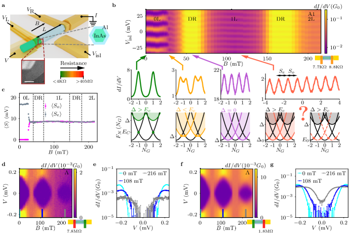
In this work we devise a method based on the tuning of junction barriers that allows to compare the results of both spectroscopy techniques by applying them to the same device. Full-shell NWs, i.e., wires covered all around by the parent superconductor, are ideal for this purpose because MZMs are predicted to appear at well defined magnetic fields [12, 38]. In addition, the superconducting full-shell largely screens the electrochemical potential of the semiconductor core from external electric fields, so that the influence of junction tuning on a potential topological phase is minimized. The scheme of our devices is depicted in Fig 1a. We use full-shell Al/InAs NWs [39] and NWs for which the Al shell has been partially etched away (dubbed partial shell devices), in order to demonstrate the breadth of our results. The atomic resolution aberration corrected (AC) high angle annular dark field (HAADF) scanning transmission electron microscopy (STEM) images indicate a perfect epitaxy of the corresponding crystal lattices (see inset of Fig 1a and Fig S1 in the supplementary information (SI)). A hybridized semiconductor-superconductor island of length is formed (see methods for fabrication details) and the transparencies of left and right junctions, consisting of bare InAs NW segments, are independently controlled by applying voltages and to the corresponding gates. The charge occupancy of the island is varied through the island gate voltage . The gate configuration allows an in-situ tuning of the barrier transparencies, which in turn control the Coulomb charging energy (where is the total capacitance of the island) [40]. For sufficient negative gate voltages it is possible to deplete the bare InAs junction and therefore switch off the devices from the left and right side independently. The transparency of the left (right) junction is characterized by the device resistance when the right (left) junction is completely on (see section 2 in the SI).
We distinguish between the island regime and the open regime. The latter has at least one very transparent barrier (colored in green) and a conductance measurement versus bias voltage and does not reveal any . For the island regime, we differentiate between the weak coupling regime (barriers colored in red) and the intermediate-coupling regime (barriers colored in orange). In the weak tunneling regime the subgap conductance at zero field is below the experimental noise level, while in the intermediate spectroscopy regime increased subgap conductance is measured due to Andreev tunneling [41].
Here we report the findings for 7 full-shell islands ranging from 200 nm to 1 , which we refer to as A (), B (), C (), D (), E (), F () and G () and 2 partial shell islands which we refer to as pA () and pB ().
We first focus on the Coulomb spectroscopy of device A (700 nm), see Fig. 1b. We investigate the Coulomb peaks in zero-bias differential conductance as a function of island gate and parallel magnetic field . The magnetic flux along the superconducting shell gives rise to the Little-Parks (LP) effect, whereby the superconducting gap is periodically modulated by the flux penetrating the NW cross section [42, 43]. The magnetic field intervals for which , called as zeroth (0L), first (1L) and second lobe (2L), alternate with intervals where , dubbed as destructive regimes (DRs). Each lobe is associated with a number of twists (or fluxoid number) of the superconducting phase around the shell, that grows by one each time the magnetic flux increases by a flux quantum .
To qualitatively understand the Coulomb blockade spectroscopy, we invoke the phenomenological energetic model [44, 45]. In thermodynamic equilibrium, the Gibbs free energy of an island with charge occupancy and dimensionless gate-induced charge , is given by:
| (1) |
where is the lever arm. We perform the Coulomb spectroscopy measurement in the regime where . For each , odd or even, has a parabolic shape when changing and the degeneracy points between two parabolas lead to Coulomb peaks in zero-bias conductance (marked as filled circles in the bottom insets of Fig. 1b). For zero magnetic field, Andreev processes give rise to coherent 2-e transport at these free energy degeneracy points as one electron drags a second one to create a Cooper pair [46] (green inset in Fig. 1b). Upon increasing the field, decreases and eventually vanishes, bringing the odd charge occupancy parabolas to zero energy. The 2-e peaks split at (orange inset in Fig. 1b) as soon as . When (DR), the island exhibits 1-e periodicity signaling metallic single electron transport (violet inset in Fig. 1b).
As we increase the field further, the superconducting LP gap reopens and the condition for 2-e transport should be restored. However, instead of 2-e, we observe 1-e periodic transport (red inset in Fig. 1b), similar to the DR transport. As a spectroscopic figure of merit, we compute the average spacing for odd and even Coulomb peaks, and , corresponding to odd or even ground states, respectively. Fig. 1c depicts and as a function of extracted from Fig. 1b. No measurable difference between and is observed in the DRs, in the 1L or in the 2L (Fig. 1c).
The 1-e transport could be explained either with a gapless superconducting island or with a subgap level of energy , such as a MZM, see red inset of Fig. 1b.
In order to clarify the validity of either of these scenarios we perform tunneling spectroscopy measurements at both ends of device A. It is important to note that there is one major difference between the two types of measurements. For Coulomb spectroscopy we need to form an island with , while for tunneling spectroscopy we need to tune one of the junctions to the open regime in order to suppress .
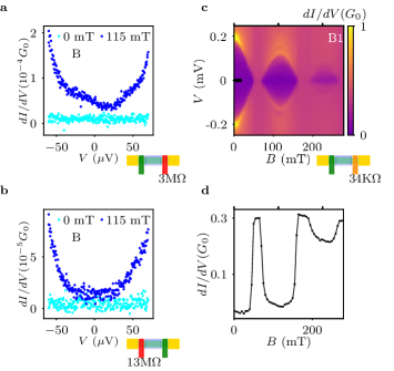
In Fig. 1d we tune to the open regime and to the weak coupling regime and we investigate the evolution of , as a function of and . Surprisingly, we cannot confirm at first sight
either of the two possible scenarios. We observe no measurable conductance within a hard gap that follows the LP modulation, and no trace of a ZBP in the 1L consistent with an state that could support 1-e periodic transport in CB (Fig. 1e). We then reverse the voltages at the top gates, closing and opening and perform tunneling spectroscopy at the right side (see Fig. 1f). We again note the LP modulation and no subgap conductance above the noise level of our measurement or ZBP, as highlighted by the line-traces in Fig. 1g.
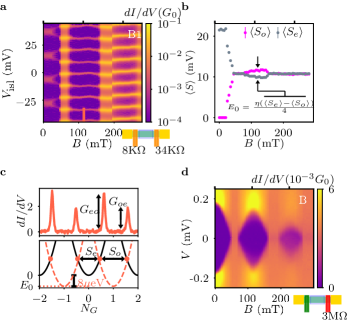
In order to understand whether the NW length has an effect on the above observations, we investigate device B which has a shorter length, , and perform again tunneling and Coulomb spectroscopy.
Figure 2a shows the Coulomb spectroscopy measurement with the tunnel barriers in the intermediate-coupling regime. Like in the previous device, the 0L is dominated by 2-e coherent transport.
Again, in the 1L the 2-e coherent transport is not recovered. Unlike the previous case where Coulomb peaks where equally spaced in the 1L, see Fig. 1c, here the Coulomb peaks exhibit an even-odd pattern (), see Figs. 2b and c. From and it is possible to extract the energy scale . In the limit of low temperatures and contact transparencies, can be interpreted as the lowest electron-like subgap level (see SI for details) [47], although this connection should be expected to break down at higher transparencies, where higher-order transport processes dominate. At the middle of the 1L we can extract an energy of eV (Fig. 2c bottom), i.e., very close to zero energy. Due to finite temperature in the experiment, a subgap level with such a small energy scale would lead to a broadened but visible ZBP in tunneling spectroscopy, since the Fermi broadening is about 15 eV in our experiment (the effective electron temperature is about 50mK). However, the tunneling spectroscopy measurements in the weak tunneling regime from both island sides do not reveal any ZBP or other discrete subgap states in the first lobe (Fig. 2d and SI).
4 Controlling the even-odd asymmetry
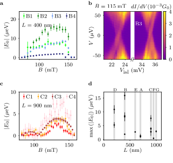
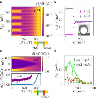
To further investigate the nature of the even-odd modulation of the Coulomb peaks, we perform the same Coulomb spectroscopy experiment for different junction resistances of device B. In Fig. 3a we plot the absolute value of as a function of taken in the 1L for four different junction configurations (B1, B2, B3 and B4; see Table ST3 for details about the junction resistances). Clearly, the voltages applied to the junctions strongly influence the modulation, independently of island length . For instance, at , can be tuned from above (configuration B2) to (configuration B4). Figure 3b furthermore demonstrates that transport takes place through a discrete resonance at low , which is separated from a continuum at higher bias. However, we note that the observation or not of such a ZBP depends on the barrier configuration (see section 11 in the SI). In Fig. 3c we repeat the same analysis for device C, a long island device with . Also for this device, it is possible to tune at from (configuration C4) to (configuration C1).
As a next step, we compare all the devices and all the configurations in terms of the maximum value of in the 1L. Fig. 3d shows as a function of , with each grey column indicating the same device but different junction resistance configurations, see also Fig. S22. Once more, one observe that the junction resistances have an influence on comparable to the island length. A complementary figure of merit that could shed light on the potential presence of MZMs is the height difference between the odd Coulomb peak , and the even one , see top panel of Fig. 2c. Similarly, the peak height modulation strongly depends on junction properties (see SI).
5 Theory and discussion
In this final section we develop a theoretical picture, a variation of the gapless superconductor scenario, that resolves the apparent conflict between transport and CB spectroscopy. We focus on the following key experimental observations: (1) the follows the LP effect but is otherwise rather featureless within the lobes; (2) the measured CB conductance peak spacing corresponds to a e charging periodicity in most of the lobe, but is otherwise e-periodic, with an even-odd modulation in corresponding to an energy scale that depends strongly on sample and barrier configuration.
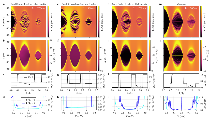
Our model of the islands follows closely the formalism of Ref. [12] (see Methods and SI). It allows us to simulate both the local density of states (LDOS) at any point of the island in a closed/closed barrier configuration (we choose a point inside the island adjacent to the left barrier), and also the transport for closed/open islands. The results are summarized in Fig. 4. We first compute the subgap spectrum of a closed/closed nm-long island in a regime of high density and relatively small induced superconducting pairing on core states. We include spin-orbit coupling (SOC), and choose a g-factor . At zero magnetic field the longitudinally quantized normal-state levels inside the core are pushed away from zero energy due to the shell-induced pairing. However, a finite magnetic flux quickly breaks the induced pairing, which leads to a dense quasicontinuum of energy levels crossing zero in lobes, and even close to the edges of the lobe. This is consistent with the kind of unmodulated 1e-periodic CB phenomenology of device A, see 1(b,c), which would follow from the gapless metallic-like subgap quasicontinuum in the closed/closed small pairing regime (so , understood as the energy of the lowest non-interacting excitation).
As the right barrier is opened to perform tunneling spectroscopy, the quasicontinuum of states is deconfined into the normal lead, smearing out the LDOS in the lobes into a weak uniform background inside the gap. Its uniformity is the result of strongly suppressed normal reflection at the right contact, made possible by the smallness of the pairing and the low normal resistance of the right barrier. The weak, uniform LDOS becomes visible in our simulations as a small but finite increase with of the zero-temperature subgap conductance background, see Fig. 4(b-d). Note that this increase was not detected in the measurements of Figs. 1 and 2, an apparent conflict that will be addressed later on.
The regime of high density and small pairing above explains the CB spectroscopy of samples with , like samples A or F. The emergence of a finite in other samples can be understood by considering a different regime with a shorter length and/or a lower electronic density. In this case, the subgap states acquire a larger level spacing, see Fig. 4e. The lowest of these longitudinally confined states has now a finite energy , around at its maximum in this instance. fluctuates strongly and stochastically with magnetic field and, notably, with barrier configuration, as the latter directly affects its longitudinal quantization condition, see Sec. 13.4 of the SI. Despite the complex LDOS dominated by mesoscopic fluctuations, and similar to the case of high density, opening the right barrier leads to a featureless with no visible trace of , see Fig. 4(f-h). The increase in conductance background is much smaller in this case, but is still present. A third plausible scenario, also with a finite , is shown in Fig. 4(i-l). In this regime, both density and induced pairing are high, but exhibits a much smaller dependence of with barrier configuration, as it is dominated by the induced pairing, see SI. In summary, the range of behaviors of our model is consistent with the large variability of in our experiments. It also supports our observation that tends to decrease for longer islands, as also found in other experiments [12].
The above phenomenology is in stark contrast to the one expected in a topological island with Majorana bound states. The topological regime, as discussed in Ref. [12], is achieved by appropriate tuning of density and SOC. In Figs. 4(m-p) we have chosen a chemical potential in a topological phase and SOC has been artificially increased 25-fold, as required to suppress the Majorana splitting across the nm island. The LDOS exhibits two Majorana bound states pinned to . The left Majorana is localized close to the left barrier, so it is not significantly broadened upon opening the right barrier, unlike the right Majorana that readily delocalizes into the reservoir [48, 49]. The zero-temperature shows a strong zero-bias anomaly, of universal height in the limit of zero temperature and splitting, in contrast to the non-topological regimes in Figs. 4(b,f). Note, however, that at finite temperatures and deep in the tunneling regime, the peak height can be strongly reduced, so reducing tunnel resistance may be required to observe it [50].
The validity of our theoretical interpretation for the small or zero energy is contingent on the existence of a weak subgap background in the tunneling that increases in lobes relative to . This background increase stems from sequential tunneling through the LDOS quasicontinuum, that is ultimately responsible for the modulated 1-e periodicity of CB spectroscopy. (An -independent cotuneling background is also expected for smaller .) Our initial measurements failed to reveal this background increase. To verify the consistency of our interpretation we revisit the measurements of versus by increasing the resolution and decreasing the noise floor. As shown in Fig. 5(a,b), this allows us to detect a small but clear increase in subgap background conductance in the 1L as compared to the 0L (tunneling in device B measured from left and the right contacts, respectively), as expected from our theory. The effect is also visible in the intermediate-coupling regime, see Figs. 5(c,d) and 4(b,c). Intermediate coupling softens the gap, but often also reveals subgap states similar to those in Fig. 4j, see SI. We note that the absence of a ZBP in the intermediate-coupling spectroscopy discards also the possibility that a MZM was not detected due to thermal broadening.
Finally, we investigate the generality of our findings by applying our experimental protocol to partial-shell NWs. Fig. 6a show the zero bias as a function of and for device pA (configuration pA1). As expected, the LP effect does not take place, and the superconducting gap gradually decreases till around 300 mT, where . The zero bias transport is 2-e periodic from 0 mT to 110 mT. At this point the 2-e Coulomb peaks split and develop an even-odd pattern, which becomes 1-e periodic at around 300 mT where superconductivity is completely destroyed. Fig. 6b depicts and as a function of extracted from Fig. 6a. It is clear that from to , whereas for higher values of the field the transport becomes 1-e periodic. The extracted (see below) is below and should be therefore observed as a ZBP. Similar to the full-shell devices, no ZBPs are observed in the tunneling spectroscopy measurement (see Fig. 6c). Similarly, no states appear in intermediate-coupling spectroscopy carried out with the same junction resistance as in Fig. 6a, see Fig. S16.
These observations support the previous findings from the full-shell devices that the the origin of the observed parity oscillations are not MZMs, but longitudinally-confined states brought down to low energies by the magnetic field through orbital effects. The orbital mechanism was also studied in Ref. [33] in the context of CB for partial-shell islands. For the sake of completeness, we studied the modulation for different barrier resistances also for the partial-shell devices. Fig. 6d shows as a function of for 4 configurations of device pA. Again, can be dramatically tuned by the junction resistances. Device pB, which shows similar behavior, is discussed in the SI (Fig. S36).
In summary, we have shown that 1-e Coulomb peak spacing results from a quasi-continuous subgap spectrum at finite field. Junction-dependent longitudinal confinement may lead to even-odd CB spacing modulation without visible low bias peaks in tunneling spectroscopy. Our work highlights the importance of junction details, even without quantum dot formation [20], for understanding transport spectroscopy in the quest for topological MZMs. Since topological edge states should theoretically be insensitive to such details, combined measurements on the same device like the ones presented here are an important step towards reducing ambiguities in interpretation. Length-dependence studies of MZM protection should take into account the possibility of junction-dependent longitudinally-confined modes as potential MZM false positives, and carefully discern algebraic () from exponential decays of even-odd modulations with length (see Fig. S42) [12, 13].
Methods
Fabrication
We use full-shell NWs which offer advantages in the search of MZMs, as they are predicted to appear at well defined magnetic fields [12, 38]. In addition, the superconducting full-shell largely screens the electrochemical potential of the semiconductor core from external electric fields. The hexagonal InAs NWs, with a diameter of about , were grown via the vapor-liquid-solid (VLS) technique and the Al shell was epitaxially grown in situ, giving a highly transparent semiconductor-SC interface [39]. The NWs were deposited on a heavily doped silicon substrate covered with of silicon oxide. The superconducting island is formed by selectively etching Al from both sides of the NW (for the partial shell devices Al is also removed from some NW facets.) The bare InAs segments at the edges of the island are used as tunnel barriers. In all devices the tunnel junction length was chosen to be below 120 nm, in order to avoid a QD formation in the tunnel barrier regions [20]. The island gates and contacts consist of normal-metal (/ Ti/Au bilayer). Two type of devices have been fabricated with top gates and with side gates. For the first type, a thick layer of aluminium oxide is added at 150 ∘C by plasma atomic layer deposition, followed by deposition of normal-metal top gates (/ Ti/Au bilayer). For the second type, the side gates are fabricated together with the ohmic contacts and the layout of the gates can be found in Fig.S27.
Device sampling/Short junction effect
Approximately 110 devices showed current at mK temperature when applying a voltage to the source and measuring a current through the drain. The tunnel junctions of the realized devices were purposefully fabricated in the short-junction limit in order to suppress QD formation [20] (see SI for device details). However, 18 of those showed ABS in at least one of the junctions and were therefore discarded. Furthermore, 78 did not show the required junction tunability, which we attribute to the short channel effect [51]. Finally 10 devices showed split Coulomb peaks and poisoning and were not further studied. The remaining 9 were fully characterized and are the focus of the present work.
Theory model
Full-shell nanowires were modeled as an axially symmetric, internal InAs semiconducting core of radius nm, covered by a 25nm-thick epitaxial Al superconducting shell. The electron subbands in the core are classified by their total angular momenta and remain decoupled in our model. The shell induces radial band bending and increased carrier density as one approaches the core/shell interface at . Additionally, the shell induces superconducting correlations on core states by the proximity effect. The induced pairing within lobe acquires the same fluxoid number of the parent Al order parameter, . The absolute strength of the induced pairing depends on interface transparency, and is assumed here to be the most relevant difference between samples. The island is coupled to normal leads through nm-long potential barriers that can be tuned from tunneling to transparent regimes. This model allows us to simulate both the local density of states (LDOS) at any point of the island in a closed/closed barrier configuration, and also the transport for closed/open islands. Both calculations are performed within a non-interacting electron approximation using the Quantica.jl package [52]. Further details on the model are provided in the SI.
Acknowledgment
The authors thank P. Krogstrup for providing us with the NW materials. Furthermore, we thank A. Higginbotham, E. J. H. Lee, C. Marcus and S. Vaitiekėnas for helpful discussions.
Funding. This research was supported by the Scientific Service Units of ISTA through resources provided by the MIBA Machine Shop and the nanofabrication facility; the NOMIS Foundation; the Spanish Ministry of Economy and Competitiveness through Grants FIS2017-84860-R, PCI2018-093026 (FlagERA Topograph) and PGC2018-097018-BI00 (AEI/FEDER, EU), the Comunidad de Madrid through Grant S2018/NMT-4511 (NMAT2D-CM) and the CSIC Research Platform on Quantum Technologies PTI-001. ICN2 also acknowledges funding from Generalitat de Catalunya 2017 SGR 327. ICN2 is supported by the Severo Ochoa program from Spanish MINECO (Grant No. SEV-2017-0706) and is funded by the CERCA Programme / Generalitat de Catalunya. Part of the present work has been performed in the framework of Universitat Autònoma de Barcelona Materials Science PhD program. Authors acknowledge the use of instrumentation as well as the technical advice provided by the National Facility ELECMI ICTS, node ”Laboratorio de Microscopías Avanzadas” at University of Zaragoza. This project has received funding from the European Union’s Horizon 2020 research and innovation programme under grant agreement No 823717 – ESTEEM3. M.B. acknowledges support from SUR Generalitat de Catalunya and the EU Social Fund; project ref. 2020 FI 00103.
Author contribution. M.V., M.Bor. and G.K. designed the experiment. M.V. and M.Bor. fabricated the devices, performed the measurements and analyzed the data under the supervision of G.K.. A. H. and G. K. performed pre-characterization measurements on island devices. S.M.-S., M.Bot. and J.A. performed the HAADF STEM and EELS measurements. E.P., R.A. and P.S-J. provided theory support during and after the measurements, and developed the theoretical framework and models to analyze the experiment. E.P and P.S-J. performed the numerical simulations. M. V, M. Bor., E. P., R.A., P.S-J. and G.K. contributed to discussions and the preparation of the manuscript with input from the rest of authors.
Competing interests: The authors declare no competing interests.
Data and Materials Availability:All experimental data included in this work and related to this work but not explicitly shown in the paper will be available via the IST Austria repository [https://doi.org/10.15479/AT:ISTA:12102]. Code used for the data analysis, microscopy analysis data and the codes used for the numerical simulation can also be found at the IST Austria repository [https://doi.org/10.15479/AT:ISTA:12102].
References
- [1] Nayak, C., Simon, S. H., Stern, A., Freedman, M. & Das Sarma, S. Non-abelian anyons and topological quantum computation. Rev. Mod. Phys. 80, 1083–1159 (2008).
- [2] Beenakker, C. Search for majorana fermions in superconductors. Annual Review of Condensed Matter Physics 4, 113–136 (2013). https://doi.org/10.1146/annurev-conmatphys-030212-184337.
- [3] Aasen, D. et al. Milestones toward majorana-based quantum computing. Phys. Rev. X 6, 031016 (2016).
- [4] Aguado, R. Majorana quasiparticles in condensed matter. Riv. Nuovo Cimento 40, 523–593 (2017).
- [5] Karzig, T. et al. Scalable designs for quasiparticle-poisoning-protected topological quantum computation with majorana zero modes. Phys. Rev. B 95, 235305 (2017).
- [6] Lutchyn, R. M. et al. Majorana zero modes in superconductor–semiconductor heterostructures. Nature Reviews Materials 3, 52–68 (2018).
- [7] Prada, E. et al. From andreev to majorana bound states in hybrid superconductor–semiconductor nanowires. Nat. Rev. Phys. 2, 575–594 (2020).
- [8] Mourik, V. et al. Signatures of Majorana Fermions in Hybrid Superconductor-Semiconductor Nanowire Devices. Science 336, 1003–1007 (2012).
- [9] Das, A. et al. Zero-bias peaks and splitting in an al–inas nanowire topological superconductor as a signature of majorana fermions. Nature Physics 8, 887–895 (2012).
- [10] Deng, M. T. et al. Majorana bound state in a coupled quantum-dot hybrid-nanowire system. Science 354, 1557–1562 (2016).
- [11] Nichele, F. et al. Scaling of majorana zero-bias conductance peaks. Phys. Rev. Lett. 119, 136803 (2017).
- [12] Vaitiekėnas, S. et al. Flux-induced topological superconductivity in full-shell nanowires. Science 367, eaav3392 (2020).
- [13] Albrecht, S. M. et al. Exponential protection of zero modes in Majorana islands. Nature 531, 206–209 (2016).
- [14] Van Heck, B., Lutchyn, R. & Glazman, L. Conductance of a proximitized nanowire in the coulomb blockade regime. Physical Review B 93, 235431 (2016).
- [15] Lutchyn, R. M., Sau, J. D. & Das Sarma, S. Majorana Fermions and a Topological Phase Transition in Semiconductor-Superconductor Heterostructures. Phys. Rev. Lett. 105, 077001 (2010).
- [16] Oreg, Y., Refael, G. & von Oppen, F. Helical Liquids and Majorana Bound States in Quantum Wires. Phys. Rev. Lett. 105, 177002 (2010).
- [17] Lutchyn, R. M. et al. Majorana zero modes in superconductor–semiconductor heterostructures. Nat. Rev. Mater. 3, 52–68 (2018).
- [18] Lee, E. J. H. et al. Spin-resolved andreev levels and parity crossings in hybrid superconductor-semiconductor nanostructures. Nat. Nanotechnology 9, 79–84 (2014).
- [19] Žitko, R., Lim, J. S., López, R. & Aguado, R. Shiba states and zero-bias anomalies in the hybrid normal-superconductor anderson model. Phys. Rev. B 91, 045441 (2015).
- [20] Valentini, M. et al. Nontopological zero-bias peaks in full-shell nanowires induced by flux-tunable andreev states. Science 373, 82–88 (2021).
- [21] Prada, E., San-Jose, P. & Aguado, R. Transport spectroscopy of nanowire junctions with majorana fermions. Phys. Rev. B 86, 180503 (2012).
- [22] Kells, G., Meidan, D. & Brouwer, P. W. Near-zero-energy end states in topologically trivial spin-orbit coupled superconducting nanowires with a smooth confinement. Phys. Rev. B 86, 100503 (2012).
- [23] Liu, C.-X., Sau, J. D., Stanescu, T. D. & Sarma, S. D. Andreev bound states versus majorana bound states in quantum dot-nanowire-superconductor hybrid structures: Trivial versus topological zero-bias conductance peaks. Phys. Rev. B 96, 075161 (2017).
- [24] Fleckenstein, C., Domínguez, F., Traverso Ziani, N. & Trauzettel, B. Decaying spectral oscillations in a majorana wire with finite coherence length. Phys. Rev. B 97, 155425 (2018).
- [25] Peñaranda, F., Aguado, R., San-Jose, P. & Prada, E. Quantifying wave-function overlaps in inhomogeneous majorana nanowires. Phys. Rev. B 98, 235406 (2018).
- [26] Reeg, C., Dmytruk, O., Chevallier, D., Loss, D. & Klinovaja, J. Zero-energy andreev bound states from quantum dots in proximitized rashba nanowires. Phys. Rev. B 98, 245407 (2018).
- [27] Moore, C., Stanescu, T. D. & Tewari, S. Two-terminal charge tunneling: Disentangling majorana zero modes from partially separated andreev bound states in semiconductor-superconductor heterostructures. Phys. Rev. B 97, 165302 (2018).
- [28] Vuik, A., Nijholt, B., Akhmerov, A. R. & Wimmer, M. Reproducing topological properties with quasi-Majorana states. SciPost Phys. 7, 61 (2019).
- [29] Chen, J. et al. Ubiquitous non-majorana zero-bias conductance peaks in nanowire devices. Phys. Rev. Lett. 123, 107703 (2019).
- [30] Ahn, S., Pan, H., Woods, B., Stanescu, T. D. & Das Sarma, S. Estimating disorder and its adverse effects in semiconductor majorana nanowires. Phys. Rev. Materials 5, 124602 (2021). URL https://link.aps.org/doi/10.1103/PhysRevMaterials.5.124602.
- [31] Carrad, D. J. et al. Shadow epitaxy for in situ growth of generic semiconductor/superconductor hybrids. Advanced Materials 32, 1908411 (2020).
- [32] Shen, J. et al. Parity transitions in the superconducting ground state of hybrid insb–al coulomb islands. Nature communications 9, 1–8 (2018).
- [33] Shen, J. et al. Full-parity phase diagram of a proximitized nanowire island. Physical Review B 104, 045422 (2021).
- [34] Pendharkar, M. et al. Parity-preserving and magnetic field–resilient superconductivity in insb nanowires with sn shells. Science 372, 508–511 (2021).
- [35] Kanne, T. et al. Epitaxial pb on inas nanowires for quantum devices. Nature Nanotechnology 1–6 (2021).
- [36] Whiticar, A. et al. Coherent transport through a majorana island in an aharonov–bohm interferometer. Nature communications 11, 1–6 (2020).
- [37] het Veld, R. L. O. et al. In-plane selective area insb–al nanowire quantum networks. Communications Physics 3, 1–7 (2020).
- [38] Peñaranda, F., Aguado, R., San-Jose, P. & Prada, E. Even-odd effect and majorana states in full-shell nanowires. Phys. Rev. Research 2, 023171 (2020).
- [39] Krogstrup, P. et al. Epitaxy of semiconductor–superconductor nanowires. Nat. Mater. 14, 400–406 (2015).
- [40] Flensberg, K. Capacitance and conductance of dots connected by quantum point contacts. Physica B: Condensed Matter 203, 432–439 (1994).
- [41] Blonder, G. E., Tinkham, M. & Klapwijk, T. M. Transition from metallic to tunneling regimes in superconducting microconstrictions: Excess current, charge imbalance, and supercurrent conversion. Phys. Rev. B 25, 4515–4532 (1982).
- [42] Little, W. A. & Parks, R. D. Observation of Quantum Periodicity in the Transition Temperature of a Superconducting Cylinder. Phys. Rev. Lett. 9, 9–12 (1962).
- [43] Vaitiekėnas, S., Krogstrup, P. & Marcus, C. M. Anomalous metallic phase in tunable destructive superconductors. Phys. Rev. B 101, 060507 (2020).
- [44] Tuominen, M. T., Hergenrother, J. M., Tighe, T. S. & Tinkham, M. Experimental evidence for parity-based 2e periodicity in a superconducting single-electron tunneling transistor. Phys. Rev. Lett. 69, 1997–2000 (1992).
- [45] Higginbotham, A. P. et al. Parity lifetime of bound states in a proximitized semiconductor nanowire. Nature Physics 11, 1017–1021 (2015). 1501.05155.
- [46] Hekking, F. W. J., Glazman, L. I., Matveev, K. A. & Shekhter, R. I. Coulomb blockade of two-electron tunneling. Phys. Rev. Lett. 70, 4138–4141 (1993).
- [47] Hansen, E. B., Danon, J. & Flensberg, K. Probing electron-hole components of subgap states in coulomb blockaded majorana islands. Phys. Rev. B 97, 041411 (2018).
- [48] San-Jose, P., Cayao, J., Prada, E. & Aguado, R. Majorana bound states from exceptional points in non-topological superconductors. Sci. Rep. 6, 21427 (2016).
- [49] Avila, J., Peñaranda, F., Prada, E., San-Jose, P. & Aguado, R. Non-hermitian topology as a unifying framework for the andreev versus majorana states controversy. Communications Physics 2, 133 (2019).
- [50] Setiawan, F., Liu, C.-X., Sau, J. D. & Das Sarma, S. Electron temperature and tunnel coupling dependence of zero-bias and almost-zero-bias conductance peaks in majorana nanowires. Phys. Rev. B 96, 184520 (2017).
- [51] Yu, B., Yuan, Y., Song, J. & Taur, Y. A two-dimensional analytical solution for short-channel effects in nanowire mosfets. Electron Devices, IEEE Transactions on 56, 2357 – 2362 (2009).
- [52] San-Jose, P. Quantica.jl: a quantum lattice simulation library in the Julia language (2021). URL https://doi.org/10.5281/zenodo.4762964.