Scanning gradiometry with a single spin quantum magnetometer
Abstract
Quantum sensors based on spin defects in diamond have recently enabled detailed imaging of nanoscale magnetic patterns, such as chiral spin textures, two-dimensional ferromagnets, or superconducting vortices, based on a measurement of the static magnetic stray field. Here, we demonstrate a gradiometry technique that significantly enhances the measurement sensitivity of such static fields, leading to new opportunities in the imaging of weakly magnetic systems. Our method relies on the mechanical oscillation of a single nitrogen-vacancy center at the tip of a scanning diamond probe, which up-converts the local spatial gradients into ac magnetic fields enabling the use of sensitive ac quantum protocols. We show that gradiometry provides important advantages over static field imaging: (i) an order-of-magnitude better sensitivity, (ii) a more localized and sharper image, and (iii) a strong suppression of field drifts. We demonstrate the capabilities of gradiometry by imaging the nanotesla fields appearing above topographic defects and atomic steps in an antiferromagnet, direct currents in a graphene device, and para- and diamagnetic metals.
Nanoscale magnetic stray fields appearing at surfaces and interfaces of magnetically-ordered materials provide important insight into the local spin structure. Such stray fields are present, for example, above magnetic domains and domain walls [1], magnetic vortices [2], spin spirals [3], skyrmions [4], or topographic steps and defects [5], and often accompany other types of ordering, like ferroelectricity [6]. Similar stray fields also appear near flowing currents [7, 8] or materials with a magnetic susceptibility [9]. Therefore, stray field measurements are a general and versatile tool to study local material or device properties.
While the magnetic imaging of ferromagnetic and ferrimagnetic textures is well-established [10, 11, 12], detection of the much weaker stray fields of, for example, antiferromagnets, multiferroics or nanoscale current distribution is a relatively new development. Quantum magnetometers based on single nitrogen-vacancy (NV) centers have recently led to exciting advances in this direction [13, 14, 15, 16, 17, 18, 19]. In their standard configuration, NV magnetometers image stray fields by scanning a sharp diamond probe over the sample surface and monitoring the static shift of the NV spin resonance frequency [20, 21]. State-of-the-art scanning NV magnetometers reach a sensitivity to static fields of a few [16, 22]. This sensitivity is sufficient for imaging the domain structure of monolayer ferromagnets [23, 22, 24] and uncompensated antiferromagnets [14, 15, 16, 17], however, it remains challenging to detect the even weaker stray fields of isolated magnetic defects, spin chains or ideally compensated antiferromagnets. While higher sensitivities, on the order of , have been demonstrated using dynamic (ac) detection of fields [25, 26], this approach is limited to the few systems whose magnetization can be modulated, like isolated spins [27, 28].
Here, we demonstrate a gradiometry technique for highly sensitive imaging of static magnetization patterns. Our method relies on up-conversion of the local spatial gradient into a time-varying magnetic field using mechanical oscillation of the sensor combined with sensitive ac quantum detection. This operating principle is well known from dynamic force microscopy [29, 30] and has been explored with NV centers [21, 31, 32, 33, 34, 35] and other magnetic sensors [36, 37] in various forms, however, it has not been realized for imaging general two-dimensional magnetic samples. As a demonstration, we show that scanning gradiometry is able to resolve the nanotesla magnetic stray fields appearing above single atomic terraces in antiferromagnetic Cr2O3. Imaging of nanoscale current patterns, magnetic susceptibility in metals, and reconstruction of field maps from gradiometry data are also demonstrated.
Gradiometry technique –
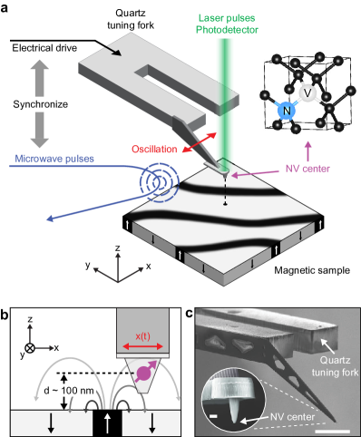
The operating principle of our gradiometry technique is shown in Fig. 1a. Our scanning magnetometer set-up consists of a sample plate that is scanned underneath a diamond probe containing a single NV center at the tip apex formed by ion implantation [38]. The diamond tip is attached to the prong of a quartz tuning fork (Fig. 1) providing atomic force microscopy (AFM) position feedback [39]. The microscope apparatus additionally includes an objective to optically polarize and read-out the NV center spin state and a bond wire acting as a microwave antenna for spin manipulation (see Methods for details). In the conventional mode of operation, we record a spin resonance spectrum at each pixel location to build up a map of the sample’s static stray field [16].
To implement the gradiometer, we mechanically oscillate the NV in a plane parallel to the sample (shear-mode) by electrically driving the tuning fork at a fixed amplitude . The NV center now experiences a time-dependent field given by
| (1) |
where is the vector component of the sample’s stray field along the NV anisotropy axis (Methods), and where describes the mechanical oscillation around the center location with frequency . The amplitudes of the , and harmonics in leading orders of are given by
| (2a) | ||||
| (2b) | ||||
| (2c) | ||||
and are therefore proportional to the static field, gradient, and second derivative, respectively. The series expansion in Eq. (2) is accurate for oscillation amplitudes smaller than the scan height, typically .
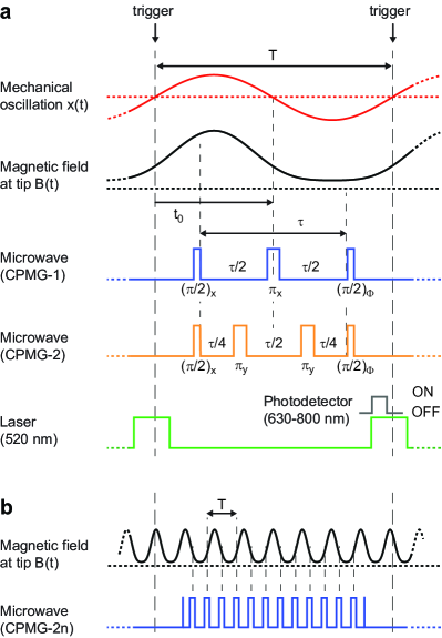
To detect the harmonics of , we synchronize the mechanical oscillation with a suitable ac quantum sensing sequence [40, 41], shown in Fig. 2a. Quantum sensing sequences measure the quantum phase accumulated by the coherent precession of a superposition of spin states during an interaction time [42]. To measure the harmonic, we invert the spin precession times during one mechanical oscillation period using microwave -pulses (Carr-Purcell-Meiboom-Gill (CPMG-) sequence [43, 42]). The pulse protocols for the first (CPMG-1) and second (CPMG-2) signal harmonic are shown in Fig. 2a. The quantum phase accumulated for the first harmonic is given by
| (3) |
where is the gyromagnetic ratio of the NV electronic spin and (see Fig. 2a). The derivation of Eq. (3) and general expressions for higher harmonics and for sequences that are off-centered with respect to the tuning fork oscillation () are given in Supplementary Note 1. To determine experimentally, we measure the photo-luminescence (PL) intensity as a function of the phase of the last microwave pulse (Fig. 2a). From the four PL signals we then extract the phase using the two-argument arc tangent (see Methods),
| (4) |
This four-phase readout technique has the advantage that the phase can be retrieved over the full range with uniform sensitivity [19, 26]. From and Eq. (3) we then compute the gradient field . Since we can only measure modulo , a phase unwrapping step is necessary for large signals that exceed the range [26].
For NV centers with long coherence times (), the sensitivity can be improved further by accumulating phase over multiple oscillation periods using CPMG- sequences (Fig. 2b). The simplest way to meet the condition is to use a mechanical oscillator with higher resonance frequency. Alternatively, as demonstrated in this work, a higher mechanical mode of the tuning fork can be employed [44]. High frequency detection has the added advantage that the interval between -pulses (given by ) becomes very short, which makes dynamical decoupling more efficient and in turn leads to improved sensitivity [41, 45]. We demonstrate single and multi-period detection schemes with sensitivities of and , respectively, in Supplementary Notes 2 and 3.
Demonstration of scanning gradiometry –
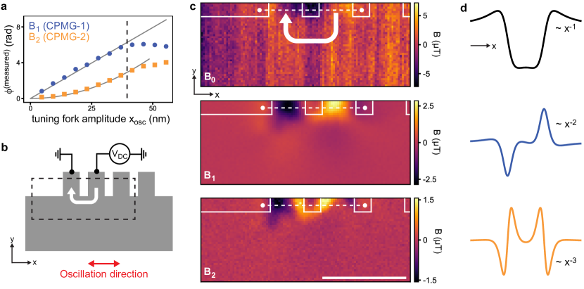
We begin measurements by calibrating the oscillation amplitude and verifying Eqs. (2,3). We characterize the gradiometry phase detection by parking the tip over a fixed position on a magnetic test sample and measuring the and signals as a function of the oscillation amplitude (see Methods and Supplementary Note 4 for characterization and calibration details). Fig. 3a confirms that the signals grow as and , as expected from the Taylor expansion (Eq. 2). Further, to avoid mixing of mechanical and field harmonic signals through surface interactions, we retract the tip by approx. from the contact point while measuring (Supplementary Note 5).
We establish two-dimensional imaging by detecting the stray field from a direct current flowing in a bilayer graphene device (Fig. 3b). This device provides an ideal test geometry because the magnetic stray field and gradient can be directly compared to the analytical model. Fig. 3c presents gradiometry maps and and, for comparison, a static field map recorded using a standard dc technique [46] with no tuning fork oscillation. Note that all images are recorded with the same imaging time and pixel size. The figure immediately highlights several advantages of gradiometry versus static field imaging: First, the signal-to-noise ratio (SNR) is strongly enhanced due to the more sensitive ac detection, despite of a lower absolute signal. Second, magnetic drift throughout the imaging time (several hours) is present in the static image but suppressed in the gradiometry images. Third, because gradient fields decay quickly with distance ( and compared to , see Fig. 3d and Supplementary Note 6), they offer a higher apparent image resolution and are thus easier to interpret.
Imaging of antiferromagnetic surface texture –
We now turn our attention to the imaging of stray fields above antiferromagnetic materials, focusing on the archetypical model system Cr2O3. Antiferromagnets represent a general class of weakly magnetic materials that are both challenging to image by existing techniques [49, 50, 51] and of key importance for understanding multiferroicity and topological magnetism in the context of antiferromagnetic spintronics [52]. Although antiferromagnets are nominally non-magnetic, weak stray fields can appear due to uncompensated moments at domain walls [14, 15, 16], spin spirals [13], topographic steps [17], or surface roughness and defects. The latter are particularly difficult to detect, yet play an important role in the pinning of domain walls [17] and establishing an exchange bias at material interfaces [53]. Careful study of these weaker fields is therefore an important avenue for quantifying the interplay between surface roughness, stray field structure, local magnetization and domain wall behavior.
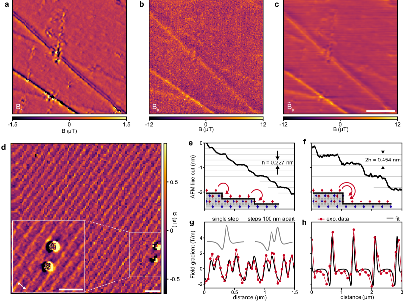
In Fig. 4a we show a gradiometry image of a polished Cr2O3 single-crystal [16]. Cr2O3 has a layered structure of out-of-plane Cr3+ moments at the (0001) surface [47, 48] that lead to stray fields at topographic steps [16, 17]. These stray fields are proportional to the step height. Indeed, Fig. 4a reveals a rich variety of magnetic anomalies on this surface, including two deep and wide topographic trenches introduced by polishing, a number of point defects, and general texture of the 2 nm-rms surface roughness (see Fig. S11 for topographic characterization). A quantitative calculation of the expected stray field maxima shows that the magnetic anomalies are well explained by the surface topography (Supplementary Note 7). Except for the trenches, these surface defects are not visible in the static field image (Fig. 4b). Note that it is possible to convert the gradiometry map into an improved static field map through integration and weighted averaging in -space (Fig. 4c and Methods).
Next, we show that gradiometry is sufficiently sensitive to detect single atomic surface steps of the layered Cr2O3(0001) surface. Fig. 4d displays a gradiometry image from a second Cr2O3 single crystal with an as-grown (unpolished) surface [47]. We observe a striking pattern of regular stripes separated by a few hundred nanometers and an approximate amplitude of . The pattern extends over the entire crystal surface with different stripe separations and directions in different regions of the sample (Fig. S12). By converting measurements into local gradients we deduce height changes (Supplementary Note 7), suggesting that the repeating striped patterns are caused by single (), or multiple atomic step edges. To corroborate, we correlate the magnetic features to the AFM topography of the sample (Fig. S12). Figs. 4e and 4f show line cuts perpendicular to the stripe direction in two regions of the sample surface, and reveal the presence of both mono- and diatomic step edges. The gradiometry data (Fig. 4g,h), are well fitted by a simple model (see Methods), producing a fitted surface magnetization of , in good agreement with earlier data [14, 16]. Together, our findings unambiguously confirm the stepped growth of the Cr2O3(0001) surface [48]. To our knowledge, our work reports the first magnetic stray field imaging of atomic steps on an antiferromagnet. It opens a complementary path to existing atomic-scale techniques, such as spin-polarized scanning tunneling microscopy and magnetic exchange force microscopy [54], without sharing the needs for an ultra-high vacuum, a conducting surface, or cryogenic operation.
Imaging of magnetic susceptibility –
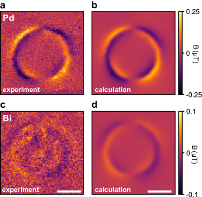
We conclude our study by demonstrating nanoscale imaging of magnetic susceptibility. Susceptometry measurements are important for investigating, for example, the magnetic response of patterned metals and materials [55, 9], superconductors [56] as well as para- and superparamagnetic nanoparticles [57, 58]. Fig. 5a shows a gradiometry map of a 50-nm-thick disc made from paramagnetic Pd placed in a bias field of . Under the bias field, the disc develops a magnetization of , where is the magnetic susceptibility of the Pd film. A fit to the data (see Methods), shown in Fig. 5b, produces a susceptibility of . This is slightly smaller than the value of pure Pd ( [59]). The decreased susceptibility may be attributed to either a finite-size effect [60] or hydrogen adsorption [61]. Repeating the same experiment with Bi, a diamagnetic sample, produces an experimental value of , which matches the accepted room temperature value of [59]. Despite the weaker susceptibility, the magnetic pattern is clearly visible and its sign inverted compared to the paramagnetic Pd disc. Additionally, local structure is apparent at the center of the disc that is explained by a variation in the film thickness (Fig. S13). Together, Fig. 4a-d demonstrate the feasibility of extending sensitive dc susceptometry to the nanometer scale.
Conclusions – In conclusion, our work demonstrates a simple yet powerful method for the imaging of static magnetization patterns with high sensitivity and spatial resolution. While we demonstrate scanning gradiometry on a layered antiferromagnet, extension to more challenging systems including perfectly compensated collinear antiferromagnets, screw and step dislocations [5], or isolated magnetic defects is natural. In particular, the magnetic signal from an atomic step edge is equivalent to that of a one-dimensional spin chain with a linear magnetization density of (Methods), demonstrating the feasibility of imaging generic 1D spin systems. Gradiometry is also well-positioned for imaging the internal structure of domain walls and skyrmions, and in particular, for quantifying their size and chirality [62, 63, 16, 64] (Supplementary Fig. S14). Finally, although we demonstrate gradiometry on magnetic fields, the technique can be extended to electric fields by orienting the external bias magnetic field perpendicular to the NV axis [65, 66, 67]. In particular, the dynamic mode of operation may alleviate charge screening that has previously limited scanning NV electrometry of dc electric field sources [68]. With the ability to image both magnetic and electric fields, one could imagine correlating antiferromagnetic and ferroelectric order in multiferroics [52], providing a unique angle to investigate the magneto-electric coupling in these fascinating and technologically important materials.
Acknowledgments
The authors thank P. Scheidegger, S. Diesch, S. Ernst, K. Herb and M. S. Wörnle for fruitful discussions, J. Rhensius for help with the Pd and Bi micro-disc fabrication and for the scanning electron micrograph in Fig. 1c, M. Giraldo and M. Fiebig for providing the Cr2O3 samples, P. Gambardella for helpful comments on the manuscript, and the staff of the FIRST lab cleanroom facility for technical support. This work was supported by the European Research Council through ERC CoG 817720 (IMAGINE), Swiss National Science Foundation (SNSF) Project Grant No. 200020_175600, the National Center of Competence in Research in Quantum Science and Technology (NCCR QSIT), and the Advancing Science and TEchnology thRough dIamond Quantum Sensing (ASTERIQS) program, Grant No. 820394, of the European Commission. M. T. acknowledges the Swiss National Science Foundation under Project No. 200021-188414.
Author contributions
C.L.D., W.S.H. and M.L.P. conceived the idea and developed the theory. W.S.H., M.L.D. and M.L.P. implemented the scanning gradiometry technique, carried out the magnetometry experiments and performed the data analysis. P.W. provided technical support with the magnetometry experiments. M.T. performed the atomic force microscopy of the unpolished Cr2O3 crystal. M.L.P. prepared the bilayer graphene sample. C.-H. L. prepared the Pd and Bi micro-discs. C.L.D. supervised the work. W.S.H. and C.L.D. wrote the manuscript. All authors discussed the results.
Competing interests
The authors declare no competing interests.
Additional information
Supplementary information accompanies this paper. Correspondence and requests for materials should be addressed to C.L.D.
Methods
Experimental set-up
All experiments were carried out at room temperature with two home-built scanning microscopes. Micro-positioning was carried out by closed-loop three-axis piezo stages (Physik Instrumente) and AFM feedback control was carried out by a lock-in amplifier (HF2LI, Zurich Instruments) and standard PID controls. PL of the NV centers was measured with avalanche photodiodes (APDs) (Excelitas) and data were collected by standard data acquisition cards (PCIe-6353, National Instruments). Direct currents sent through the bilayer graphene were created with an arbitrary waveform generator (DN2.663-04, Spectrum Instrumentation) and the current was measured with a transimpedance amplifier (HF2TA, Zurich Instruments). Microwave pulses and sequences were created with a signal generator (Quicksyn FSW-0020, National Instruments) and modulated with an IQ mixer (Marki) and an arbitrary waveform generator (DN2.663-04, Spectrum Instrumentation and HDAWG, Zurich Instruments). NV centers were illuminated at by a custom-designed pulsed diode laser. Scanning NV tips were purchased from QZabre AG [38]. Three different NV tips were used throughout this study with stand-off distances between (excluding the 20 nm retract distance).
Magnetic samples
Bilayer graphene device: Standard microfabrication processes were used, including mechanical exfoliation and a dry transfer process for generating the hBN-bilayer-graphene-hBN stack, electron beam lithography and plasma etching for creating the device geometry and physical vapor deposition for creating the metallic device contacts. Full details can be found in Ref. 26.
Cr2O3 crystals: The mechanically polished and non-polished Cr2O3 bulk single crystals were provided by Prof. Manfred Fiebig. Both crystals have a (0001) surface orientation. Crystal growth and processing details can be found in Refs. 16, 47.
Pd and Bi discs: Metallic micro-discs were created using standard microfabrication processes. Discs were defined through electron beam lithography on spin-coated Si wafers. Chemical development of the spin-coated resist, followed by metal deposition of either 50 nm of Pd or Bi and a lift-off process finished the fabrication.
Initialization and readout of NV spin state
A laser pulse of duration was used to polarize the NV center into the state. Then, the dc or ac quantum sensing measurement occurred on the to transition (see below). The readout of the NV’s spin state was performed by another long laser pulse, during which the photons emitted from the NV center were collected with the APD, binned as a function of time, and summed over a window () that optimized spin-state-dependent PL contrast [69].
DC sensing protocol
DC magnetic images were acquired with the pulsed ODMR method [46]. Obtained magnetic resonance spectra were fitted for the center frequency of a Lorentzian function, , where is the spin contrast (in percent) and is the width of the Lorentzian dip. In a 2D scan the magnetic field projected along the axis of the NV could be determined at each pixel using where is the resonance frequency far from the surface. For our diamond probes, the NV anisotropy axis was at an angle with respect to the out-of-plane direction (-axis in Fig. 1). Therefore, corresponded to the vector field projection along this tilted direction.
AC sensing protocol
AC sensing used either a spin echo and or dynamical decoupling sequence [40, 41]. The NV spin state was initialized optically into the state followed by a microwave -pulse to create a coherence between the and states. The quantum phase accumulated between the two states during the coherent precession can be expressed as where is the modulation function [42], is the magnetic field, is the interaction time (the time in between the first and last -pulse), and where we use the rotating frame approximation. The modulation function alternates between with each microwave -pulse during the pulse sequence. While imaging with the gradiometry pulse sequences, -pulses were sometimes used instead of the final -pulses for the projective spin readout to reduce pulse imperfections caused by (ca. ) drifts in the NV resonance frequency.
Calibration of tuning fork oscillation
We estimated the oscillation amplitude and oscillation angle in the -plane, denoted by , of the tuning forks with two different in-situ measurement techniques. The first method involved processing a static field map and a gradient field map acquired over the same region with a least-squares minimization scheme. By minimizing a cost function proportional to the pixel differences between the and numerically differentiated images, estimates for and were determined. The second method involved a stroboscopic imaging of the static field () synchronized to the tuning fork oscillation. By measuring the time-tagged displacements of magnetic features recorded at different positions during the tuning fork oscillation, and could be estimated by fitting to the path taken by the NV. We found that scaled linearly with the applied drive voltage for the voltages we used while imaging. Examples of these calibration methods are given in Supplementary Note 4.
Calibration of the trigger delay
In order to optimize the ac sensing sequences, and to distinguish between signals from the first and second derivatives (see Supplementary Note 1), a trigger delay () calibration measurement must be made. The calibration measurement consisted of measuring the phase at a stationary point on the sample, while varying , thus producing a phase that oscillated as a function of . The chosen value of was the value which maximized the measured phase. Examples of this calibration measurement, as well as the characterization of PL oscillation caused by the tuning fork motion, are shown in the Supplementary Note 4.
Reconstruction of the static field map from the gradient map
A gradient map can be used to reduce the noise and improve the image of a (less sensitive) static field map . Letting denote the true static magnetic field value, the experimentally measured and field maps are
| (5) |
where is the directional derivative and and are white noise added to each pixel (reflecting the Poissonian shot noise of the photo-detection). In -space these equations can be transformed into
| (6) |
where denotes the Fourier transform of , is the dot product between the oscillation direction and the -vector . Integration in -space introduces a -dependent noise term in the gradient field map. In particular, the integrated gradient map has noise amplification near the line but has noise suppression far away from that line. Directional sensitivity could be avoided by oscillating the tuning fork in the -direction (tapping mode), or by using an oscillator that supports orthogonal lateral modes. To circumvent this problem we average two -space maps (Eq. 6) with -vector dependent weights that reflect the noise added by the integration process. The use of inverse variance weights additionally results in an image with the lowest possible variance. Thus, the optimal reconstructed static field map can be computed by taking the inverse Fourier transform of
| (7) |
where defines a cut-off wave vector determined by the oscillation amplitude and the noise variances and . The corresponding cut-off wavelength reflects the spatial wavelength above (below) which the () field map is less noisy. It should also be noted that the -space averaging process can be modified to include the map, however the map provides the most significant improvement. Specifically, in Fig. 4c, and were used as reconstruction parameters (determined by the calibration in Supplementary Note 4). Note, since the gradient and -space averaging are directional, the noise reduction is also directional (approximately in the -direction and in the -direction).
Stray fields from atomic step edges
For an atomic step edge propagating along the -direction the stray field is modeled by two out-of-plane magnetic samples with different heights. Taking the analytical form (see Ref. 62) for the stray fields above an edge at as , , and , where is the surface magnetization, we define the stray field produced by a small change in the height as
| (8) |
with . The expressions are simplified in the limit of since the sub-nanometer atomic step edges are much smaller than typical standoff distances of . We measure the gradient of the stray field along the oscillation direction, taken as the -direction for simplicity. This leads to field gradients of
| (9) |
The fits in Fig. 4g and 4h are produced by projecting the field gradients onto the NV axis defined by and summing over multiple steps. The line cuts are produced by rotating and plane averaging a 2D image (Fig. S12). We account for the rotation angle in the -plane by introducing an additional image rotation angle . The experimentally measured field is then fitted by
| (10) |
We set and for the fit in Fig. 4g, and for the fit in Fig. 4h and fixed (determined by the tip calibration) in both fits. The standoff distance , the surface magnetization , angles and and step edge locations are free parameters in the fit. Collectively, the fitted line scans give (including the retract distance) and , which is consistent with previous measurements on this sample [16].
Note, Eq. 8 is functionally equivalent to the magnetic field from a one-dimensional ferromagnetic spin chain with a linear magnetization density of . To demonstrate this, we calculate the stray field produced by a infinite line of magnetic dipoles along the line and pointing in the -direction as:
| (11) |
where .
Susceptibility fitting for Pd and Bi discs
Susceptibility fits followed the assumption that the stray field produced by a para- or diamagnetic sample is identical to that of a homogeneously magnetized body with a magnetization magnitude of and a magnetization vector that is parallel to the external polarizing field. The stray field produced by this magnetization is where is the magnetic potential. We computed the stray field using the -space method of Ref. [70] and fitted the gradient image to the numerically computed gradient fields. In the fitting procedure we fixed , (determined by the tip calibration) and sample thickness while the standoff distance , magnetization magnitude , angles and , circle radius and position are free parameters in the fit. The susceptibilities are computed as and the fitted magnetizations were and .
References
- Rondin et al. [2012] L. Rondin, J. P. Tetienne, P. Spinicelli, C. dal Savio, K. Karrai, G. Dantelle, A. Thiaville, S. Rohart, J. F. Roch, and V. Jacques, Nanoscale magnetic field mapping with a single spin scanning probe magnetometer, Appl. Phys. Lett. 100, 153118 (2012).
- Shinjo et al. [2000] T. Shinjo, T. Okuno, R. Hassdorf, K. Shigeto, and T. Ono, Magnetic vortex core observation in circular dots of permalloy, Science 289, 930 (2000).
- Cox et al. [1963] D. Cox, W. Takei, and G. Shirane, A magnetic and neutron diffraction study of the Cr2O3-Fe2O3 system, Journal of Physics and Chemistry of Solids 24, 405 (1963).
- Yu et al. [2010] X. Yu, Y. Onose, N. Kanazawa, J. Park, J. Han, Y. Matsui, N. Nagaosa, and Y. Tokura, Real-space observation of a two-dimensional skyrmion crystal, Nature 465, 901 (2010).
- Ravlić et al. [2003] R. Ravlić, M. Bode, A. Kubetzka, and R. Wiesendanger, Correlation of dislocation and domain structure of Cr(001) investigated by spin-polarized scanning tunneling microscopy, Physical Review B 67, 10.1103/physrevb.67.174411 (2003).
- Fiebig et al. [2002] M. Fiebig, T. Lottermoser, D. Frohlich, A. V. Goltsev, and R. V. Pisarev, Observation of coupled magnetic and electric domains, Nature 419, 818 (2002).
- Chang et al. [2017] K. Chang, A. Eichler, J. Rhensius, L. Lorenzelli, and C. L. Degen, Nanoscale imaging of current density with a single-spin magnetometer, Nano Letters 17, 2367 (2017).
- Tetienne et al. [2017] J. P. Tetienne, N. Dontschuk, D. A. Broadway, A. Stacey, D. A. Simpson, and L. C. L. Hollenberg, Quantum imaging of current flow in graphene, Sci Adv 3, e1602429 (2017).
- Bluhm et al. [2009] H. Bluhm, J. A. Bert, N. C. Koshnick, M. E. Huber, and K. A. Moler, Spinlike susceptibility of metallic and insulating thin films at low temperature, Phys. Rev. Lett. 103, 026805 (2009).
- Hopster and [Eds.] H. Hopster and H. P. O. (Eds.), Magnetic Microscopy of Nanostructures (Springer, Berlin, 2005).
- Freeman and Choi [2001] M. R. Freeman and B. C. Choi, Advances in magnetic microscopy, Science 294, 1484 (2001).
- Hartmann [1999] U. Hartmann, Magnetic force microscopy, Annu. Rev. Mater. Sci. 29, 53 (1999).
- Gross et al. [2017] I. Gross, W. Akhtar, V. Garcia, L. J. Martinez, S. Chouaieb, K. Garcia, C. Carretero, B. Arthelemy, P. Appel, P. Maletinsky, J. V. Kim, J. Y. Chauleau, N. Jaouen, M. Viret, M. Bibes, S. Fusil, and V. Jacques, Real-space imaging of non-collinear antiferromagnetic order with a single-spin magnetometer, Nature 549, 252 (2017).
- Appel et al. [2019] P. Appel, B. J. Shields, T. Kosub, N. Hedrich, R. Hubner, J. Fassbender, D. Makarov, and P. Maletinsky, Nanomagnetism of magnetoelectric granular thin-film antiferromagnets, Nano Lett. 19, 1682 (2019).
- Wornle et al. [2019] M. S. Wornle, P. Welter, Z. Kaspar, K. Olejnik, V. Novak, R. P. Campion, P. Wadley, T. Jungwirth, C. L. Degen, and P. Gambardella, Current-induced fragmentation of antiferromagnetic domains, arXiv:1912.05287 (2019).
- Wornle et al. [2021] M. S. Wornle, P. Welter, M. Giraldo, T. Lottermoser, M. Fiebig, P. Gambardella, and C. L. Degen, Coexistence of bloch and neel walls in a collinear antiferromagnet, Phys. Rev. B 103, 094426 (2021).
- Hedrich et al. [2021] N. Hedrich, K. Wagner, O. V. Pylypovskyi, B. J. Shields, T. Kosub, D. D. Sheka, D. Makarov, and P. Maletinsky, Nanoscale mechanics of antiferromagnetic domain walls, Nature Physics 17, 064007 (2021).
- Jenkins et al. [2020] A. Jenkins, S. Baumann, H. Zhou, S. A. Meynell, D. Yang, K. Watanabe, T. Taniguchi, A. Lucas, A. F. Young, and A. C. B. Jayich, Imaging the breakdown of ohmic transport in graphene, arXiv:2002.05065 (2020).
- Ku et al. [2020] M. J. H. Ku, T. X. Zhou, Q. Li, Y. J. Shin, J. K. Shi, C. Burch, L. E. Anderson, A. T. Pierce, Y. Xie, A. Hamo, U. Vool, H. Zhang, F. Casola, T. Taniguchi, K. Watanabe, M. M. Fogler, P. Kim, A. Yacoby, and R. L. Walsworth, Imaging viscous flow of the Dirac fluid in graphene, Nature 583, 537 (2020).
- Rondin et al. [2014] L. Rondin, J. P. Tetienne, T. Hingant, J. F. Roch, P. Maletinsky, and V. Jacques, Magnetometry with nitrogen-vacancy defects in diamond, Rep. Prog. Phys. 77, 056503 (2014).
- Degen [2008] C. L. Degen, Scanning magnetic field microscope with a diamond single-spin sensor, Appl. Phys. Lett. 92, 243111 (2008).
- Sun et al. [2021] Q. Sun, T. Song, E. Anderson, A. Brunner, J. Forster, T. Shalomayeva, T. Taniguchi, K. Watanabe, J. Grafe, R. Stohr, X. Xu, and J. Wrachtrup, Magnetic domains and domain wall pinning in atomically thin CrBr3 revealed by nanoscale imaging, Nature Communications 12, 1989 (2021).
- Thiel et al. [2019] L. Thiel, Z. Wang, M. A. Tschudin, D. Rohner, I. Gutierrez-lezama, N. Ubrig, M. Gibertini, E. Giannini, A. F. Morpurgo, and P. Maletinsky, Probing magnetism in 2D materials at the nanoscale with single-spin microscopy, Science 364, 973 (2019).
- Fabre et al. [2021] F. Fabre, A. Finco, A. Purbawati, A. Hadj-Azzem, N. Rougemaille, J. Coraux, I. Philip, and V. Jacques, Characterization of room-temperature in-plane magnetization in thin flakes of CrTe2 with a single-spin magnetometer, Phys. Rev. Materials 5, 034008 (2021).
- Vool et al. [2021] U. Vool, A. Hamo, G. Varnavides, Y. Wang, T. X. Zhou, N. Kumar, Y. Dovzhenko, Z. Qiu, C. A. C. Garcia, A. T. Pierce, J. Gooth, P. Anikeeva, C. Felser, P. Narang, and A. Yacoby, Imaging phonon-mediated hydrodynamic flow in WTe2, Nature Physics 10.1038/s41567-021-01341-w (2021).
- Palm et al. [2022] M. L. Palm, W. S. Huxter, P. Welter, S. Ernst, P. J. Scheidegger, S. Diesch, K. Chang, P. Rickhaus, T. Taniguchi, K. Wantanabe, K. Ensslin, and C. L. Degen, Imaging of sub-A currents in bilayer graphene using a scanning diamond magnetometer, arXiv:2201.06934 (2022).
- Rugar et al. [2004] D. Rugar, R. Budakian, H. J. Mamin, and B. W. Chui, Single spin detection by magnetic resonance force microscopy, Nature 430, 329 (2004).
- Grinolds et al. [2014] M. S. Grinolds, M. Warner, K. de Greve, Y. Dovzhenko, L. Thiel, R. L. Walsworth, S. Hong, P. Maletinsky, and A. Yacoby, Subnanometre resolution in three-dimensional magnetic resonance imaging of individual dark spins, Nat. Nano. 9, 279 (2014).
- Hillenbrand et al. [2000] R. Hillenbrand, M. Stark, and R. Guckenberger, Higher-harmonics generation in tapping-mode atomic-force microscopy: insights into the tip-sample interaction, Appl. Phys. Lett. 76, 3478 (2000).
- Sahin et al. [2007] O. Sahin, C. Quate, O. Solgaard, and F. Giessibl, Higher-harmonic force detection in dynamic force microscopy, Springer Handbook of Nanotechnology , 717 (2007).
- Hong et al. [2012] S. Hong, M. S. Grinolds, P. Maletinsky, R. L. Walsworth, M. D. Lukin, and A. Yacoby, Coherent mechanical control of a single electronic spin, Nano Lett. 12, 3920 (2012).
- Kolkowitz et al. [2012] S. Kolkowitz, A. C. B. Jayich, Q. P. Unterreithmeier, S. D. Bennett, P. Rabl, J. G. E. Harris, and M. D. Lukin, Coherent sensing of a mechanical resonator with a single-spin qubit, Science 335, 1603 (2012).
- Teissier et al. [2014] J. Teissier, A. Barfuss, P. Appel, E. Neu, and P. Maletinsky, Strain coupling of a nitrogen-vacancy center spin to a diamond mechanical oscillator, Phys. Rev. Lett. 113, 020503 (2014).
- Esquinazi et al. [2015] P. D. Esquinazi, J. Meijer, and F. Jelezko, Method and device for the determination of static electric and / or static magnetic fields and the topology of components by means of a sensor technology based on quantum effects, Patent Application DE102015016021A1 (2015).
- Wood et al. [2018] A. A. Wood, A. G. Aeppli, E. Lilette, Y. Y. Fein, A. Stacey, L. C. L. Hollenberg, R. E. Scholten, and A. M. Martin, -limited sensing of static magnetic fields via fast rotation of quantum spins, Phys. Rev. B 98, 174114 (2018).
- Uri et al. [2020] A. Uri, Y. Kim, K. Bagani, C. K. Lewandowski, S. Grover, N. Auerbach, E. O. Lachman, Y. Myasoedov, T. Taniguchi, K. Watanabe, J. Smet, and E. Zeldov, Nanoscale imaging of equilibrium quantum Hall edge currents and of the magnetic monopole response in graphene, Nature Physics 16, 164 (2020).
- Wyss et al. [2021] M. Wyss, K. Bagani, D. Jetter, E. Marchiori, A. Vervelaki, B. Gross, J. Ridderbos, S. Gliga, C. Schonenberger, and M. Poggio, Magnetic thermal and topographic imaging with a nanometer-scale squid-on-cantilever scanning probe, arXiv:2109.06774 (2021).
- [38] QZabre Ltd., https://qzabre.com, .
- Giessibl [1998] F. J. Giessibl, High-speed force sensor for force microscopy and profilometry utilizing a quartz tuning fork, Appl. Phys. Lett. 73, 3956 (1998).
- Taylor et al. [2008] J. M. Taylor, P. Cappellaro, L. Childress, L. Jiang, D. Budker, P. R. Hemmer, A.Yacoby, R. Walsworth, and M. D. Lukin, High-sensitivity diamond magnetometer with nanoscale resolution, Nat. Phys. 4, 810 (2008).
- Lange et al. [2011] G. D. Lange, D. Riste, V. V. Dobrovitski, and R. Hanson, Single-spin magnetometry with multipulse sensing sequences, Phys. Rev. Lett. 106, 080802 (2011).
- Degen et al. [2017] C. Degen, F. Reinhard, and P. Cappellaro, Quantum sensing, Rev. Mod. Phys. 89, 035002 (2017).
- Meiboom and Gill [1958] S. Meiboom and D. Gill, Modified spin-echo method for measuring nuclear relaxation times, Rev. Sci. Instr. 29, 688 (1958).
- Zeltzer et al. [2007] G. Zeltzer, J. C. Randel, A. K. Gupta, R. Bashir, S.-H. Song, and H. C. Manoharan, Scanning optical homodyne detection of high-frequency picoscale resonances in cantilever and tuning fork sensors, Applied Physics Letters 91, 173124 (2007).
- Ryan et al. [2010] C. A. Ryan, J. S. Hodges, and D. G. Cory, Robust decoupling techniques to extend quantum coherence in diamond, Phys. Rev. Lett. 105, 200402 (2010).
- Dreau et al. [2011] A. Dreau, M. Lesik, L. Rondin, P. Spinicelli, O. Arcizet, J. F. Roch, and V. Jacques, Avoiding power broadening in optically detected magnetic resonance of single NV defects for enhanced dc magnetic field sensitivity, Phys. Rev. B 84, 195204 (2011).
- Fiebig [1996] M. Fiebig, Nichtlineare spektroskopie und topografie an antiferromagnetischen domänen, PhD Thesis (1996).
- He et al. [2010] X. He, Y. Wang, N. Wu, A. N. Caruso, E. Vescovo, K. D. Belashchenko, P. A. Dowben, and C. Binek, Robust isothermal electric control of exchange bias at room temperature, Nature Materials 9, 579 (2010).
- Fiebig et al. [1995] M. Fiebig, D. Fröhlich, G. Sluyterman v. L., and R. V. Pisarev, Domain topography of antiferromagnetic by second-harmonic generation, Applied Physics Letters 66, 2906 (1995).
- Scholl et al. [2000] A. Scholl, J. Stöhr, J. Lüning, J. W. Seo, J. Fompeyrine, H. Siegwart, J.-P. Locquet, F. Nolting, S. Anders, E. E. Fullerton, M. R. Scheinfein, and H. A. Padmore, Observation of antiferromagnetic domains in epitaxial thin films, Science 287, 1014 (2000).
- Wu et al. [2011] N. Wu, X. He, A. L. Wysocki, U. Lanke, T. Komesu, K. D. Belashchenko, C. Binek, and P. A. Dowben, Imaging and control of surface magnetization domains in a magnetoelectric antiferromagnet, Physical Review Letters 106, 10.1103/physrevlett.106.087202 (2011).
- Cheong et al. [2020] S. W. Cheong, M. Fiebig, W. Wu, L. Chapon, and V. Kiryukhin, Seeing is believing: visualization of antiferromagnetic domains, npj Quantum Materials 5, 10.1038/s41535-019-0204-x (2020).
- Nogués et al. [1999] J. Nogués, T. J. Moran, D. Lederman, I. K. Schuller, and K. V. Rao, Role of interfacial structure on exchange-biased FeF2-Fe, Physical Review B 59, 6984 (1999).
- Wiesendanger [2009] R. Wiesendanger, Spin mapping at the nanoscale and atomic scale, Rev. Mod. Phys. 81, 1495 (2009).
- Gardner et al. [2001] B. W. Gardner, J. C. Wynn, P. G. Bjornsson, E. W. J. Straver, K. A. Moler, J. R. Kirtley, and M. B. Ketchen, Scanning superconducting quantum interference device susceptometry, Rev. Sci. Instr. 72, 2361 (2001)).
- Low et al. [2021] D. Low, G. M. Ferguson, A. Jarjour, B. T. Schaefer, M. D. Bachmann, P. J. W. Moll, and K. C. Nowack, Scanning squid microscopy in a cryogen-free dilution refrigerator, Rev. Sci. Instr. 92, 083704 (2021).
- Gould et al. [2014] M. Gould, R. J. Barbour, N. Thomas, H. Arami, K. M. Krishnan, and K. C. Fu, Room-temperature detection of a single 19 nm super-paramagnetic nanoparticle with an imaging magnetometer, Appl. Phys. Lett. 105, 072406 (2014).
- Fescenko et al. [2019] I. Fescenko, A. Laraoui, J. Smits, N. Mosavian, P. Kehayias, J. Seto, L. Bougas, A. Jarmola, and V. M. Acosta, Diamond magnetic microscopy of malarial hemozoin nanocrystals, Phys. Rev. Applied 11, 034029 (2019).
- [59] D. R. L. (editor), CRC Handbook of Chemistry and Physics, 84th Edition, J. Am. Chem. Soc. 126, 1586 (2004).
- Macfarlane et al. [2013] W. A. Macfarlane, T. J. Parolin, T. I. Larkin, G. Richter, K. H. Chow, M. D. Hossain, R. F. Kiefl, C. D. P. Levy, G. D. Morris, O. Ofer, M. R. Pearson, H. Saadaoui, Q. Song, and D. Wang, Finite-size effects in the nuclear magnetic resonance of epitaxial palladium thin films, Phys. Rev. B 88, 144424 (2013).
- Jamieson and Manchester [1972] H. C. Jamieson and F. D. Manchester, The magnetic susceptibility of Pd, PdH and PdD between 4 and 300K, Journal of Physics F: Metal Physics 2, 323 (1972).
- Tetienne et al. [2015] J. P. Tetienne, T. Hingant, L. J. Martinez, S. Rohart, A. Thiaville, L. H. Diez, K. Garcia, J. P. Adam, J. V. Kim, J. F. Roch, I. M. Miron, G. Gaudin, L. Vila, B. Ocker, D. Ravelosona, and V. Jacques, The nature of domain walls in ultrathin ferromagnets revealed by scanning nanomagnetometry, Nat. Commun. 6, 6733 (2015).
- Dovzhenko et al. [2018] Y. Dovzhenko, F. Casola, S. Schlotter, T. X. Zhou, F. Buttner, R. L. Walsworth, G. S. D. Beach, and A. Yacoby, Magnetostatic twists in room-temperature skyrmions explored by nitrogen-vacancy center spin texture reconstruction, Nature Communications 9, 2712 (2018).
- Velez et al. [2022] S. Velez, S. R. Gomez, J. Schaab, E. Gradauskaite, M. S. Wornle, P. Welter, B. J. Jacot, C. L. Degen, M. Trassin, M. Fiebig, and P. Gambardella, Current-driven dynamics and ratchet effect of skyrmion bubbles in a ferrimagnetic insulator, submitted (2022).
- Dolde et al. [2011] F. Dolde, H. Fedder, M. W. Doherty, T. Noebauer, F. Rempp, G. Balasubramanian, T. Wolf, F. Reinhard, L. C. L. Hollenberg, F. Jelezko, and J. Wrachtrup, Electric-field sensing using single diamond spins, Nat. Phys. 7, 459 (2011).
- Barson et al. [2021] M. S. J. Barson, L. M. Oberg, L. P. Mcguinness, A. Denisenko, N. B. Manson, J. Wrachtrup, and M. W. Doherty, Nanoscale vector electric field imaging using a single electron spin, Nano Lett. 21, 2962 (2021).
- Bian et al. [2021] K. Bian, W. Zheng, X. Zeng, X. Chen, R. Stohr, A. Denisenko, S. Yang, J. Wrachtrup, and Y. Jiang, Nanoscale electric-field imaging based on a quantum sensor and its charge-state control under ambient condition, Nature Communications 12, 2457 (2021).
- Oberg et al. [2020] L. Oberg, M. de Vries, L. Hanlon, K. Strazdins, M. S. Barson, M. Doherty, and J. Wrachtrup, Solution to electric field screening in diamond quantum electrometers, Phys. Rev. Applied 14, 014085 (2020).
- Schirhagl et al. [2014] R. Schirhagl, K. Chang, M. Loretz, and C. L. Degen, Nitrogen-vacancy centers in diamond: Nanoscale sensors for physics and biology, Annu. Rev. Phys. Chem. 65, 83 (2014).
- Beardsley [1989] I. A. Beardsley, Reconstruction of the magnetization in a thin film by a combination of Lorentz microscopy and external field measurements, IEEE Transactions on Magnetics 25, 671 (1989).