Topological bands in the PdSe2 pentagonal monolayer
Abstract
The electronic structure of monolayer pentagonal palladium diselenide (PdSe2) is analyzed from the topological band theory perspective. Employing first-principles calculations, effective models and symmetry indicators, we find that the low-lying conduction bands are topologically nontrivial, protected by time reversal and crystalline symmetries. Numerical evidence supporting the nontrivial character of the bands is presented. Furthermore, we obtain a relevant physical response from the topological viewpoint, such as the spin Hall conductivity.
I Introduction
Two-dimensional (2D) materials are among the most promising types of systems in the continuous search for novel structures that can give shape to future technological advances. The low-dimensional character of these structures makes them ideal candidates for their application in nanoscale devices [1]. Starting with graphene more than a decade ago, a vast amount of these layered systems has been proposed [2, 3, 4]. Within this emerging group of novel 2D systems, pentagonal 2D materials are attracting increasing attention because of their symmetry. For instance, the proposal of pentagraphene stirred much attention [5, 6, 7, 8]. Furthermore, the possibility of presenting topologically nontrivial phases has driven the interest to other pentagonal layers with different compositions [9, 10, 11, 12]. However, some theoretical proposals have been shown to be structurally unstable, specially those with dominant p-orbital bonds [13, 14]. Notwithstanding, there are several instances of experimentally found 2D pentamaterials, such as PdSe2, PdS2 and NiN2 [15, 16, 17]. Among these, the recently synthesized PdSe2 has been the subject of intensive experimental and theoretical research. Importantly, the pentagonal phase is the stable allotrope for this material. Different forms of pentagonal PdSe2 with a variable number of layers have been reported, possessing high air stability [18, 19, 20, 21, 22], which is an essential characteristic for their extended (long-term) use. Also, electrical transport characteristics [23], remarkable optical [24, 25, 26, 27], and good thermoelectric properties [28] have been experimentally reported. On the theoretical side, several works have analyzed the physical properties of the material in its monolayer and multilayer form [29, 30, 31, 32, 33]. Among these theoretical accounts the band connectivity and the symmetry-related properties of the electronic structure have not been studied in detail for monolayer PdSe2; we address this issue in this work. Using the theory of symmetry indicators along with first-principles calculations, we identify that the lowest conduction bands of monolayer PdSe2 realize a topologically nontrivial phase. These bands comprise a strong topological phase with a well defined topological invariant and gapless edges states that we characterize using well-known numerical methods. Also, an analysis on the accessibility of these nontrivial conduction states by Fermi level manipulation is presented. These results open the possibility for the exploration of this promising material and its related structures from the topological point of view.
The article is organized as follows. First, an overview of the numerical calculations and parameters used is sketched. This is followed by the geometric information and first-principles electronic band structure of monolayer PdSe2, along with a study of the symmetry character of the bands. Additionally, effective models based on Wannier interpolation are briefly described and put forward to study the edge states and the Wannier charge center (WCC) evolution along different directions. The spin Hall conductivity, a signature of its nontrivial band character, is computed as a function of frequency and chemical potential. Finally, we conclude with a summary and outlook for possible future avenues to explore the potential of this material. Part of our results are left as Electronic Supplementary Information (ESI)†.
II Computational details
The calculations for the band structure were carried with standard density functional theory (DFT) method using the QUANTUM ESPRESSO (QE) package [34] at the GGA (generalized gradient approximation) level within the Perdew-Burke-Ernzerhof (PBE) implementation. We have also corroborated the robustness of our main results by resorting to the GPAW code [35, 36] and checking for several DFT functionals; these additional computations are summarized in Appendix A. The monolayer structure was relaxed with a force tolerance of eV/Å. The energy cutoff for the plane wave basis was 100 Ry with a vacuum distance of 20 Å in the perpendicular direction to the monolayer. A Monkhorst-Pack grid of was chosen and the energy convergence tolerance was set to Ry. The Wannier interpolation of the DFT energy bands was performed with the Wannier90 code [37]. Two models were implemented; a twelve-band (12B) model including the four uppermost valence band and the eight lowest conduction bands, and an eight-band (8B) model that only includes the above-mentioned conduction bands. This latter model was used to focus only on the nontrivial bands of the system. For the 12B model, -orbitals were used for the Pd atoms and -orbitals for the Se atoms. These orbitals were only used as starting sites for the orbitals, since the location of the Wannier centers may change under the wannierization process. The post-processing of Wannier-based models was carried by the PythTB code [38]. Also, Wannier90 was used to analyze this model and to calculate the optical responses presented below. The mathematical expressions implemented in this code are based on Refs. [39, 40] and for quick reference are presented in the ESI.†
III Electronic band structure and symmetry indicators
III.1 Lattice geometry and space group
The lattice structure of PdSe2 is composed of irregular (type 2) pentagons forming a buckled geometry as presented in Fig. 1 a) [41]. Pd atoms are fourfold coordinated and Se atoms have coordination three. As previous works reported [18], the crystalline order conforms a tetragonal lattice, with three symmetry operations; a twofold rotation around one of the lattice vectors axis with fractional translation (1/2,1/2,0) in terms of the unit cell vectors, a mirror glide plane and spatial inversion [42]. This has to be complemented with time reversal (TR) symmetry to give the space group (SG) P21c or SG #14. The Pd atoms sit at the Wickoff position (WP) while the Se atoms locate at the WP [42]. The relaxed structure obtained from first-principles calculations comprises a rectangular unit cell with lattice vectors with magnitude Å and Å. The calculation also yields a puckering distance of 0.7 Å, confirming the buckled geometry of the material. These results show a good agreement with the reported experimental and theoretical values [29, 33, 18, 43]. The band structure of monolayer PdSe2 has been extensively studied in previous works [18, 29, 30, 31, 32, 33, 43]. As indicated above, we have also carried out an extensive investigation of its electronic properties by employing several exchange-correlation functionals, detailed in Appendix A. We confirm the robustness of the nontrivial topology found for this material.
Here we focus on the band connectivity an associated topological properties of the low-energy bands around the Fermi level. For this purpose we present in Fig. 1 c) the electronic band structure including spin-orbit coupling (SOC) at the PBE level along the high-symmetry path in momentum space. The Brillouin zone is depicted in Fig. 1 b), following the notation of Ref.[44].
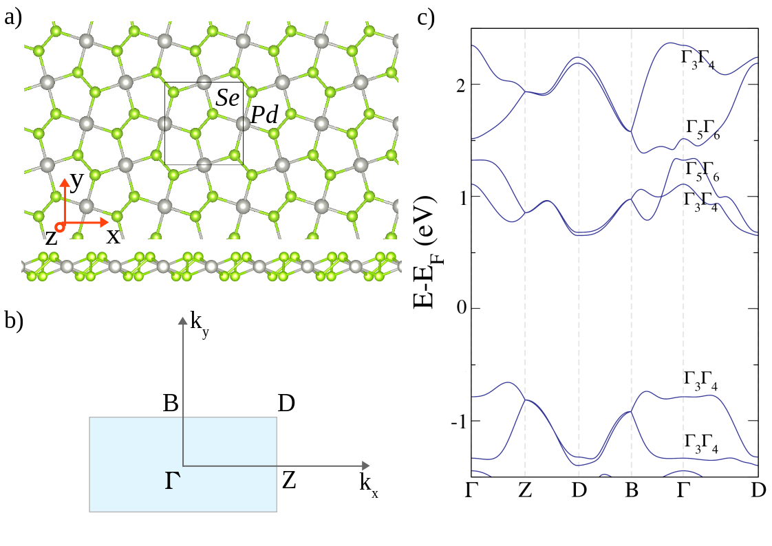
The inclusion of SOC is crucial for the results obtained as will be clarified in what follows. It is well-known that PBE functionals systematically underestimate the fundamental gap in semiconductors and insulators. As stated above, we verified that other functionals yield similar results and predict the nontrivial topology found with QE, as detailed in the Appendix. Additionally, we have revised the existing literature concerning the electronic structure of monolayer PdSe2 obtained with the hybrid (HSE06) functional [30] and at the GW level [45]. These more expensive calculations show a larger band gap but also keep the band general features unaltered, giving validity for the topological analysis using the PBE functional presented here.
From the band structure and the space group information it can be confirmed that all bands are doubly degenerate along the whole Brillouin zone (BZ) since monolayer PdSe2 is centrosymmetric (SG#14). The spin-orbit interaction - which requires the use of double space groups - obviously affects the degeneracies of the system without SOC, only leaving the possibility of fourfold nodal points at the Z and B points. These points are protected by the nonsymmorphic symmetries of the SG in conjunction with time-reversal symmetry [46], and they are present in every group of four bands in the structure. This is the basic ingredient for the band connectivity of the system, since these sets of four bands form a band representation [47], following the prescription of topological quantum chemistry theory and symmetry-based indicators [48, 49, 50].
The first step in the study of the topological properties of monolayer PdSe2 is the identification of nontrivial topology signatures in the corresponding space group, namely, SG #14. Firstly, it is customary to look for strong topology, since this is the most widely known nontrivial phase. To this end, we employ the results of Ref. [51], adapted for the case of a two dimensional BZ. Specifically, a Smith normal form decomposition is applied to the set of elementary band representations (EBR) of the SG. Recall that EBR are the building blocks to construct the bands of atomic insulators and as such, they can be mapped directly to exponentially localized Wannier functions [52] situated at the atomic positions of the material. The procedure is briefly sketched as follows. First an EBR matrix is constructed, including as coefficients the multiplicities of the irreducible representations (IR) at the high-symmetry points of the material (, Z, D and B for our particular case). The elements of the EBR matrix are provided in Table 1 (using the Bilbao Crystallographic Server information [44]). Next, the Smith normal form matrix is calculated, which is a diagonal matrix with positive integer values. If some of these values are greater that one, then a strong topological phase is possible for the SG [51]. The matrix for the (2D) SG#14 is given by
| (1) |
| IR/EBR | EBR1 | EBR2 | EBR3 | EBR4 |
|---|---|---|---|---|
| 2 | 2 | 0 | 0 | |
| 0 | 0 | 2 | 2 | |
| D3 | 1 | 0 | 1 | 0 |
| D4 | 1 | 0 | 1 | 0 |
| D5 | 0 | 1 | 0 | 1 |
| D6 | 0 | 1 | 0 | 1 |
| Z2 | 1 | 1 | 1 | 1 |
| B2 | 1 | 1 | 1 | 1 |
We observe that a diagonal element with value 2 is present, which allows for a phase in the system [51]. Thus, strong topological bands are in principle possible in this SG. This phase is a version of the time-reversal plus inversion topological phase [53], which in this case is further enriched by the other crystalline symmetries of the group. The presence of these additional symmetries simplifies the symmetry-indicated character of the nontrivial topology. This can be seen in the definition of the above mentioned invariant. Further manipulation of the EBR matrix (see the ESI† for this particular group or Ref. [51] for the general theory) gives as a result that the invariant only depends on the parity of the point IR. In this double SG only has two IR, and [54]. With this definition the topological invariant for the strong phase can be defined as
| (2) |
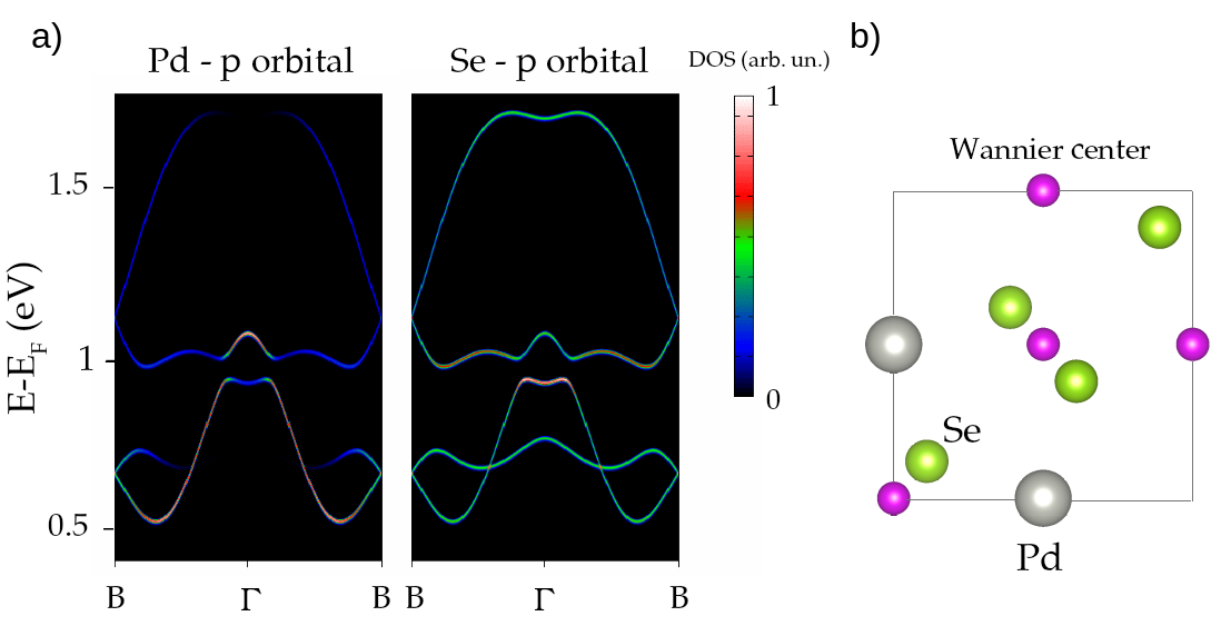
where correspond to the multiplicities of the IR at . In other words, if a single (fourfold) band representation or a group of band representations has an odd number of IR, then these bands are topological. This definition of is simpler than the standard Fu-Kane formula for TR inversion-symmetric insulators [55] due to the additional constraints of the above-mentioned symmetries. Note that this is the only kind of symmetry-indicated topology that can be present in this two-dimensional (layer) version of SG#14. The linear combination of strong band representations may yield either a strong band or a trivial band representation. This differs from the three-dimensional version of this group, where fragile bands and strong bands can coexist [51]. We have numerically computed the IR characters for monolayer PdSe2 from the first-principles electronic structure using the IrRep package [56]. We consider two groups of bands: the valence band manifold of the material and the eight lowest conduction bands. In the valence band set there exists an even number of irreducible representations, which render the material a trivial insulator. On the other hand, if we take into account the aforementioned conduction bands, we find that both fourfold band representations have separately an odd number of IR. Therefore, each single group realizes a strong topological group of bands. In Fig. 1 c) we have labeled the highest valence band and the lowest conduction bands with the corresponding IR. A crucial role here is played by the SOC, which permits a band inversion between the two group of band representations. The inversion can be initially identified from the band structure in Fig. 1 c), specially along the line. Further confirmation of this band inversion is presented in Fig.2 a), where the orbital-projected bands are presented. The -orbitals constitute the most important contribution to the inversion and the effective models for these bands are based on this result.
III.2 Evidence of the nontrivial topology
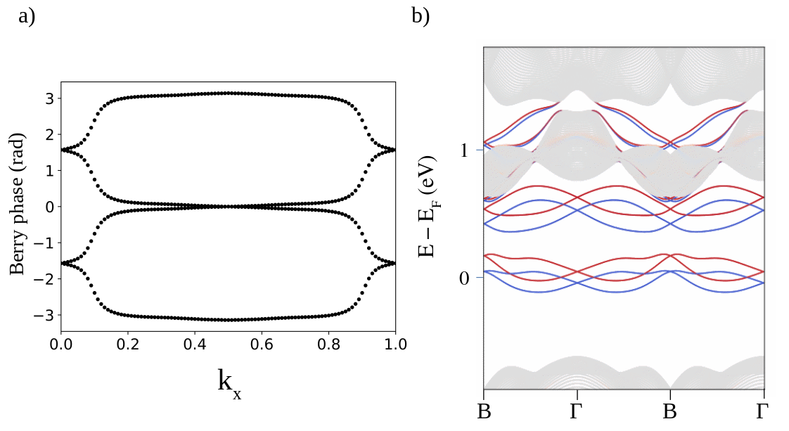
A clearer picture of the nontrivial topology of monolayer PdSe2 can be obtained by the computation of the standard quantities that pinpoint the nontrivial character of the bands. Thus, we calculated the energy dispersion for a ribbon geometry of the material and the bulk Wannier charge center (WCC) evolution along the BZ [57], using a Wannier-based model. Before delving into these results, we would like to comment on the Wannier centers in real space associated with the conduction bands. We employed a reduced 8B model, as described above, to account only for these bands. They are well separated from the higher conduction bands, which make them suitable for faithful wannierization. The localization of the Wannier centers in real space for PdSe2 is represented in Fig. 2 b). A pair of Wannier centers sits on each site, as dictated by time reversal symmetry (Kramers pairs) [58]. Most importantly, it can be observed that two pairs of these Wannier centers are localized at a WP (2b) that is not occupied by any of the atoms in the material. This obstruction hints for a nontrivial topology [58] and PdSe2 can be dubbed as a conduction-band-obstructed atomic insulator. The other Wannier centers localize on the 2a WP and thus coincide with atomic (Pd) orbitals. The WCC evolution along the direction in the BZ is presented in Fig3 a). Here we also use the 8B model in order to isolate the nontrivial behavior. For this model we assume that the four lowest conduction bands are occupied, just to conform with the usual WCC definition [52]. The general trend of the WCC evolution shows the typical features of a TR inversion-symmetric topological insulator [53], with the nontrivial crossings at one of the time-reversal invariant momenta (in this case ). The energy dispersion of the edge states for a confined geometry is plotted in Fig. 3 b). In this case we make use of the 12B model, with the aim to show the fundamental gap and their edge states. Gapless energy states arise within the gap at eV above the Fermi level, localized on the edges of the finite slab, giving further confirmation for the nontrivial phase of the conduction bands. The edge termination has influence on the dispersion of the edge states, but there are always gapless states in this upper gap. The fundamental gap also presents edge states that are trivial in terms of the above classification. Further information for other edges is presented in the ESI†.
IV Topologically relevant physical response
The main drawback of the topological bands spotted in the above discussion is that they are situated in the conduction bands, which implies that some external manipulation of the material is necessary in order to access them. This hinders the use of monolayer PdSe2 as a spin Hall insulator, since the nontrivial gap is not the fundamental gap. Notwithstanding, the lowest conduction bands of the material are reachable by standard doping and gating [59, 1]. Nowadays there are gating techniques for 2D materials which allows for higher doping levels than standard methods [60, 61]. As these procedures can displace the chemical potential to lie inside the conduction bands, it is possible to access the nontrivial bands and explore the nontrivial behavior of the material. We simulate this electron doping effect by a rigid shift of the chemical potential using the 12B model and calculate an optical response, namely,
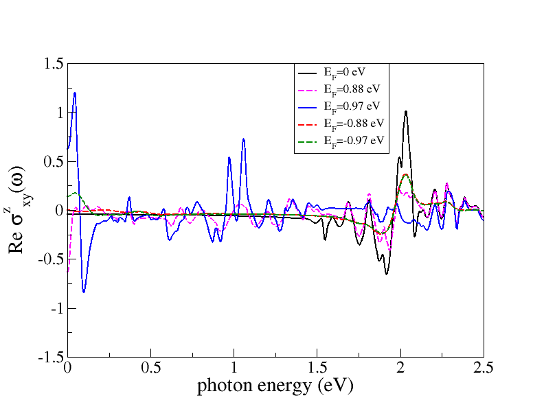
the frequency-dependent spin Hall conductivity (SHC) for different values of the chemical potential. The slab geometry has been taken into account by a global scaling factor following Ref. [39]. We report the real part in Fig. 4; only the usual component with spin along the direction and transverse current with respect to the applied external field is presented. We have calculated cases with the chemical potential within the conduction band and also inside the trivial valence bands to assess the magnitude of the response. Additionally, the SHC with no doping effect is included. It can be appreciated that both types of doping produce a new intense peak in the low-frequency range of the spectrum. However, when is situated around the nodal features of the conduction bands - around 1 eV above the original Fermi level - the magnitude of this peak is greatly enhanced, giving additional support to the nontrivial character of the bands. Although the topological character is not essential for an enhanced magnitude of the effect, as can be checked by the large static SHC in Pt [62], it can boost the optical response. Several other works have reported sizable values for two-dimensional semiconductors [63, 64]. It is important to note that the above-mentioned optical effect could be affected by the inclusion of quasiparticle effects, such as those discussed in Ref. [30] for the linear optical response.
Additionally, from Fig. 4 it can be observed that the static limit () of the optical SHC yields a nonzero value even for the undoped system, implying a nonzero SHC within the fundamental gap. This situation has been encountered in previous calculations of the SHC on semiconductors such as in Refs. [65, 66], where it is mentioned that the in-gap SHC cannot give rise to spin accumulation for trivial systems. Recently [64], it has been argued that this SHC is only a numerical artifact due to the use of a broadening factor and, by means of degenerate perturbation theory, they obtain zero in-gap conductivities for trivial insulators. For completeness we have computed this static SHC for monolayer PdSe2, using the method of Ref. [64] as implemented in Ref. [67], and also with the Wannier90 code [40], which uses the standard broadening factor. In both cases we obtain a constant nonzero value along both the trivial and the nontrivial gap. Yet, the magnitude in the case of the trivial gap is low and in principle could not be detectable. This static SHC is presented in the ESI†.
V Conclusions
In this work we address the electronic band topology of monolayer PdSe2. We have shown that, although the valence bands of the material are trivial and in principle the system is a trivial topological insulator, the lowest conduction bands have a nontrivial topology. By means of standard analysis we have found that the group of lowest fourfold-degenerated conduction bands are separately nontrivial, characterized by a invariant. This phase is strong and gives rise to gapless edge states in the conduction band gap and to a nontrivial WCC evolution. The nontrivial character of these bands can be in principle accessible by doping, and we have presented numerical evidence for enhanced responses in the case of the optical spin Hall conductivity at low frequency. It can be mentioned that other materials with the same pentagonal structure and space group in monolayer form has been theoretically reported in several computational databases [68, 69]. Many of these materials - such as for example PtTe2, PdTe2 and NiTe2 - show a similar behavior for the low-lying conduction bands and are expected to host similar nontrivial bands. Further work is also needed to elucidate other connections between the nontrivial bands and physical responses not covered here. Additionally, topological bands could likely be present in multilayer PdSe2 and their effects for the low energy regime are worth to be explored.
Appendix: Electronic characterization of PdSe2 monolayer
In this section we present the theoretical electronic characterization of the PdSe2 monolayer, i.e., the electronic band structure computed within a first-principles approach with different exchange-correlation functionals. The calculations are performed in the framework of density functional theory (DFT) as implemented in GPAW using several GGA and van der Waals (vdW) exchange-correlation functionals [35, 36]. A projected augmented wave (PAW) method was employed for the basis set with an energy cutoff of eV. For the -points we used a grid of . All structures are fully relaxed until the atomic forces in each atom were less of eV/Å.
| XC | a(Å) | b(Å) | gap (eV) | group # |
|---|---|---|---|---|
| PBE | 5.84960 | 5.90720 | 1.108 | 14 |
| LDA | 5.73997 | 5.78863 | 1.171 | 14 |
| RPBE | 5.89355 | 5.95226 | 1.086 | 14 |
| revPBE | 5.88490 | 5.93966 | 1.094 | 14 |
| vdW-DF | 5.96822 | 6.04448 | 0.943 | 14 |
| vdW-DF2 | 6.03519 | 6.03519 | 0.850 | 14 |
| optPBE-vdW | 5.90887 | 5.98340 | 0.976 | 14 |
| C09-vdW | 5.82330 | 5.89056 | 1.025 | 14 |
| GLLBSC | 1.880 | |||
| exp-bulk[15] | 5.7457 | 5.8679 |
The computed values of the lattice constants and the bandgap of the 2D pentagonal PdSe2 are shown in Table A.1. Comparing to the experimental values for bulk PdSe2 reported in Ref. [15], we observe that PBE functional shows a maximum difference of 0.05 Å for the lattice parameter. If vdW interactions are considered, the maximum difference in lattice constant is 0.26 Å for the vdW-DF2 functional, in agreement with a previous report of theoretical lattice parameters of bulk PdSe2 [15]. Independently of the geometric configuration obtained for every exchange-correlation functional, the symmetry group of monolayer PdSe2 is preserved.
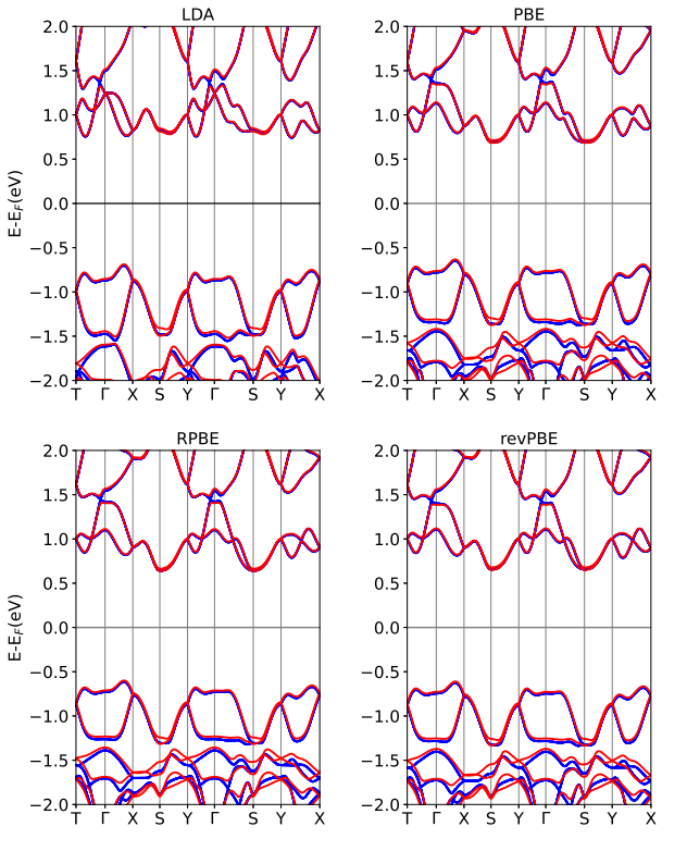
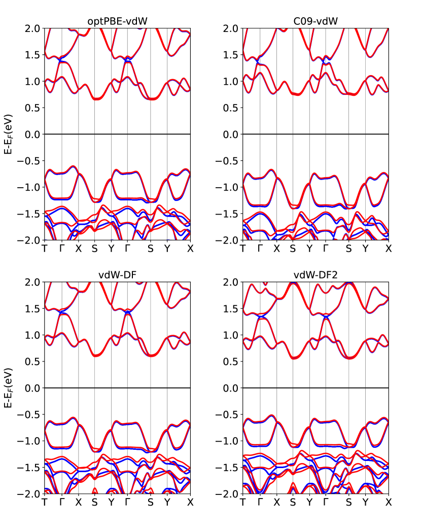
The band structures for PdSe2 monolayer are shown in Figs. A.1 and A.2. The -point path is labeled using the high-symmetry points of the of the 3D orthorhombic lattice. Our results show that, independently of the exchange-correlation functional, the topology characteristics of the bands are preserved and are the same as those obtained with QE calculations.
Acknowledgements
This work has been partially supported by Chilean FONDECYT Grant 1211913, Spanish MCIU and AEI and the European Union under Grant No. PGC2018-097018-B-I00 (MCIU/AEI/FEDER, UE), and by Grant USM-DGIIP PI-LI 1925.
References
- Fiori et al. [2014] G. Fiori, F. Bonaccorso, G. Iannaccone, T. Palacios, D. Neumaier, A. Seabaugh, S. K. Banerjee, and L. Colombo, Electronics based on two-dimensional materials, Nature Nanotechnology 9, 768 (2014).
- Miró et al. [2014] P. Miró, M. Audiffred, and T. Heine, An atlas of two-dimensional materials, Chem. Soc. Rev. 43, 6537 (2014).
- Saptarshi et al. [2015] D. Saptarshi, J. A. Robinson, M. Dubey, H. Terrones, and M. Terrones, Beyond graphene: Progress in novel two-dimensional materials and van der waals solids, Annual Review of Materials Research 45, 1 (2015).
- Novoselov et al. [2016] K. Novoselov, A. Mishchenko, A. Carvalho, and A. H. Castro Neto, 2d materials and van der waals heterostructures, Science 353, 10.1126/science.aac9439 (2016).
- Tang et al. [2014] C.-P. Tang, S.-J. Xiong, W.-J. Shi, and J. Cao, Two-dimensional pentagonal crystals and possible spin-polarized dirac dispersion relations, Journal of Applied Physics 115, 113702 (2014).
- Zhang et al. [2015] S. Zhang, J. Zhou, Q. Wang, X. Chen, Y. Kawazoe, and P. Jena, Penta-graphene: A new carbon allotrope, Proceedings of the National Academy of Sciences 112, 2372 (2015).
- Bravo et al. [2018] S. Bravo, J. Correa, L. Chico, and M. Pacheco, Tight-binding model for opto-electronic properties of penta-graphene nanostructures, Scientific Reports 8, 11070 (2018).
- Correa et al. [2020] J. Correa, M. Pacheco, S. Bravo, and L. Chico, Electronic and magnetic properties of pentagonal nanoribbons, Carbon 162, 209 (2020).
- Zhao et al. [2016] T. Zhao, S. Zhang, Y. Guo, and Q. Wang, Tic2: a new two-dimensional sheet beyond mxenes, Nanoscale 8, 233 (2016).
- Zhuang [2019a] H. L. Zhuang, From pentagonal geometries to two-dimensional materials, Computational Materials Science 159, 448 (2019a).
- Bravo et al. [2019] S. Bravo, J. Correa, L. Chico, and M. Pacheco, Symmetry-protected metallic and topological phases in penta-materials, Scientific Reports 9, 12754 (2019).
- Bravo et al. [2021] S. Bravo, M. Pacheco, V. Nuñez, J. D. Correa, and L. Chico, Two-dimensional weyl points and nodal lines in pentagonal materials and their optical response, Nanoscale 13, 6117 (2021).
- Avramov et al. [2015] P. Avramov, V. Demin, M. Luo, C. H. Choi, P. B. Sorokin, B. Yakobson, and L. Chernozatonskii, Translation symmetry breakdown in low-dimensional lattices of pentagonal rings, The Journal of Physical Chemistry Letters 6, 4525 (2015).
- Kuklin et al. [2020] A. V. Kuklin, H. Ågren, and P. V. Avramov, Structural stability of single-layer pdse2 with pentagonal puckered morphology and its nanotubes, Phys. Chem. Chem. Phys. 22, 8289 (2020).
- Oyedele et al. [2017a] A. D. Oyedele, S. Yang, L. Liang, A. A. Puretzky, K. Wang, J. Zhang, P. Yu, P. R. Pudasaini, A. W. Ghosh, Z. Liu, C. M. Rouleau, B. G. Sumpter, M. F. Chisholm, W. Zhou, P. D. Rack, D. B. Geohegan, and K. Xiao, PdSe2: Pentagonal Two-Dimensional Layers with High Air Stability for Electronics, Journal of the American Chemical Society 139, 14090 (2017a), publisher: American Chemical Society.
- Zhang et al. [2021] X. Zhang, G. Su, J. Lu, W. Yang, W. Zhuang, K. Han, X. Wang, Y. Wan, X. Yu, and P. Yang, Centimeter-scale few-layer pds2: Fabrication and physical properties, ACS Applied Materials & Interfaces 13, 43063 (2021).
- Bykov et al. [2021] M. Bykov, E. Bykova, A. V. Ponomareva, F. Tasnádi, S. Chariton, V. B. Prakapenka, K. Glazyrin, J. S. Smith, M. F. Mahmood, I. A. Abrikosov, and A. F. Goncharov, Realization of an ideal cairo tessellation in nickel diazenide nin2: High-pressure route to pentagonal 2d materials, ACS Nano 15, 13539 (2021).
- Oyedele et al. [2017b] A. D. Oyedele, S. Yang, L. Liang, A. A. Puretzky, K. Wang, J. Zhang, P. Yu, P. R. Pudasaini, A. W. Ghosh, Z. Liu, C. M. Rouleau, B. G. Sumpter, M. F. Chisholm, W. Zhou, P. D. Rack, D. B. Geohegan, and K. Xiao, PdSe : Pentagonal Two-Dimensional Layers with High Air Stability for Electronics, J. Am. Chem. Soc. 139, 14090 (2017b).
- Nguyen et al. [2020] G. D. Nguyen, A. D. Oyedele, A. Haglund, W. Ko, L. Liang, A. A. Puretzky, D. Mandrus, K. Xiao, and A.-P. Li, Atomically Precise PdSe Pentagonal Nanoribbons, ACS Nano 14, 1951 (2020).
- Fu et al. [2020] M. Fu, L. Liang, Q. Zou, G. D. Nguyen, K. Xiao, A.-P. Li, J. Kang, Z. Wu, and Z. Gai, Defects in highly anisotropic transition-metal dichalcogenide pdse2, The Journal of Physical Chemistry Letters 11, 740 (2020), pMID: 31880944.
- Xie et al. [2020] C. Xie, S. Jiang, Y. Gao, M. Hong, S. Pan, J. Zhao, and Y. Zhang, Giant thickness-tunable bandgap and robust air stability of 2d palladium diselenide, Small 16, 2000754 (2020).
- Lu et al. [2020] L.-S. Lu, G.-H. Chen, H.-Y. Cheng, C.-P. Chuu, K.-C. Lu, C.-H. Chen, M.-Y. Lu, T.-H. Chuang, D.-H. Wei, W.-C. Chueh, W.-B. Jian, M.-Y. Li, Y.-M. Chang, L.-J. Li, and W.-H. Chang, Layer-dependent and in-plane anisotropic properties of low-temperature synthesized few-layer pdse2 single crystals, ACS Nano 14, 4963 (2020), pMID: 32233458, https://doi.org/10.1021/acsnano.0c01139 .
- Oyedele et al. [2019] A. D. Oyedele, S. Yang, T. Feng, A. V. Haglund, Y. Gu, A. A. Puretzky, D. Briggs, C. M. Rouleau, M. F. Chisholm, R. R. Unocic, D. Mandrus, H. M. Meyer, S. T. Pantelides, D. B. Geohegan, and K. Xiao, Defect-Mediated Phase Transformation in Anisotropic Two-Dimensional PdSe Crystals for Seamless Electrical Contacts, J. Am. Chem. Soc. 141, 8928 (2019).
- Yu et al. [2020] J. Yu, X. Kuang, Y. Gao, Y. Wang, K. Chen, Z. Ding, J. Liu, C. Cong, J. He, Z. Liu, and Y. Liu, Direct observation of the linear dichroism transition in two-dimensional palladium diselenide, Nano Letters 20, 1172 (2020), pMID: 31944114, https://doi.org/10.1021/acs.nanolett.9b04598 .
- Yu et al. [2021] J. Yu, X. Kuang, J. Li, J. Zhong, C. Zeng, L. Cao, Z. Liu, Z. Zeng, Z. Luo, T. He, A. Pan, and Y. Liu, Giant nonlinear optical activity in two-dimensional palladium diselenide, Nature Communications 12, 1083 (2021).
- [26] X. Chen, J. Huang, C. Chen, M. Chen, G. Hu, H. Wang, N. Dong, and J. Wang, Broadband nonlinear photoresponse and ultrafast carrier dynamics of 2d pdse2, Advanced Optical Materials n/a, 2101963.
- Gudelli and Guo [2021] V. K. Gudelli and G.-Y. Guo, Large bulk photovoltaic effect and second-harmonic generation in few-layer pentagonal semiconductors PdS2 and PdSe2, New Journal of Physics 23, 093028 (2021).
- Zhao et al. [2020] Y. Zhao, P. Yu, G. Zhang, M. Sun, D. Chi, K. Hippalgaonkar, J. T. L. Thong, and J. Wu, Low-symmetry pdse2 for high performance thermoelectric applications, Advanced Functional Materials 30, 2004896 (2020).
- Sun et al. [2015] J. Sun, H. Shi, T. Siegrist, and D. J. Singh, Electronic, transport, and optical properties of bulk and mono-layer pdse2, Applied Physics Letters 107, 153902 (2015).
- Kuklin and Ågren [2019] A. V. Kuklin and H. Ågren, Quasiparticle electronic structure and optical spectra of single-layer and bilayer : Proximity and defect-induced band gap renormalization, Phys. Rev. B 99, 245114 (2019).
- Kuklin et al. [2021] A. V. Kuklin, L. V. Begunovich, L. Gao, H. Zhang, and H. Ågren, Point and complex defects in monolayer : Evolution of electronic structure and emergence of magnetism, Phys. Rev. B 104, 134109 (2021).
- Lei et al. [2020] W. Lei, W. Wang, X. Ming, S. Zhang, G. Tang, X. Zheng, H. Li, and C. Autieri, Structural transition, metallization, and superconductivity in quasi-two-dimensional layered under compression, Phys. Rev. B 101, 205149 (2020).
- Feng et al. [2020] L.-Y. Feng, R. A. B. Villaos, Z.-Q. Huang, C.-H. Hsu, and F.-C. Chuang, Layer-dependent band engineering of pd dichalcogenides: a first-principles study, New Journal of Physics 22, 053010 (2020).
- Giannozzi et al. [2020] P. Giannozzi, O. Baseggio, P. Bonfà, D. Brunato, R. Car, I. Carnimeo, C. Cavazzoni, S. de Gironcoli, P. Delugas, F. Ferrari Ruffino, A. Ferretti, N. Marzari, I. Timrov, A. Urru, and S. Baroni, Quantum espresso toward the exascale, The Journal of Chemical Physics 152, 154105 (2020).
- Mortensen et al. [2005] J. J. Mortensen, L. B. Hansen, and K. W. Jacobsen, Real-space grid implementation of the projector augmented wave method, Physical Review B 71, 035109 (2005), publisher: American Physical Society.
- Enkovaara et al. [2010] J. Enkovaara, C. Rostgaard, J. J. Mortensen, J. Chen, M. Dułak, L. Ferrighi, J. Gavnholt, C. Glinsvad, V. Haikola, H. A. Hansen, H. H. Kristoffersen, M. Kuisma, A. H. Larsen, L. Lehtovaara, M. Ljungberg, O. Lopez-Acevedo, P. G. Moses, J. Ojanen, T. Olsen, V. Petzold, N. A. Romero, J. Stausholm-Møller, M. Strange, G. A. Tritsaris, M. Vanin, M. Walter, B. Hammer, H. Häkkinen, G. K. H. Madsen, R. M. Nieminen, J. K. Nørskov, M. Puska, T. T. Rantala, J. Schiøtz, K. S. Thygesen, and K. W. Jacobsen, Electronic structure calculations with GPAW: a real-space implementation of the projector augmented-wave method, Journal of Physics: Condensed Matter 22, 253202 (2010).
- Mostofi et al. [2014] A. A. Mostofi, J. R. Yates, G. Pizzi, Y.-S. Lee, I. Souza, D. Vanderbilt, and N. Marzari, An updated version of wannier90: A tool for obtaining maximally-localised Wannier functions, Computer Physics Communications 185, 2309 (2014).
- [38] S. Coh and D. Vanderbilt, Python tight binding (pythtb), http://www.physics.rutgers.edu/pythtb/.
- Ibañez-Azpiroz et al. [2018] J. Ibañez-Azpiroz, S. S. Tsirkin, and I. Souza, Ab initio calculation of the shift photocurrent by Wannier interpolation, Phys. Rev. B 97, 245143 (2018).
- Qiao et al. [2018] J. Qiao, J. Zhou, Z. Yuan, and W. Zhao, Calculation of intrinsic spin Hall conductivity by Wannier interpolation, Phys. Rev. B 98, 214402 (2018).
- Zhuang [2019b] H. L. Zhuang, From pentagonal geometries to two-dimensional materials, Computational Materials Science 159, 448 (2019b).
- Christopher Bradley [2010] A. P. C. Christopher Bradley, The Mathematical Theory of Symmetry in Solids: Representation Theory for Point Groups and Space Groups, Oxford Classic Texts in the Physical Sciences (Oxford University Press, Oxford, New York, 2010).
- Lei et al. [2019] W. Lei, B. Cai, H. Zhou, G. Heymann, X. Tang, S. Zhang, and X. Ming, Ferroelastic lattice rotation and band-gap engineering in quasi 2d layered-structure pdse2 under uniaxial stress, Nanoscale 11, 12317 (2019).
- Aroyo et al. [2006] M. I. Aroyo, A. Kirov, C. Capillas, J. M. Perez-Mato, and H. Wondratschek, Bilbao Crystallographic Server. II. Representations of crystallographic point groups and space groups, Acta Crystallographica Section A 62, 115 (2006).
- Kim and Choi [2021] H.-g. Kim and H. J. Choi, Quasiparticle band structures of bulk and few-layer from first-principles calculations, Phys. Rev. B 103, 165419 (2021).
- Dresselhaus et al. [2008] M. S. Dresselhaus, G. Dresselhaus, and A. Jorio, Group Theory: Application to the Physics of Condensed Matter (Springer-Verlag, Berlin Heidelberg, 2008).
- Cano et al. [2018] J. Cano, B. Bradlyn, Z. Wang, L. Elcoro, M. G. Vergniory, C. Felser, M. I. Aroyo, and B. A. Bernevig, Building blocks of topological quantum chemistry: Elementary band representations, Phys. Rev. B 97, 035139 (2018).
- Cano and Bradlyn [2021] J. Cano and B. Bradlyn, Band representations and topological quantum chemistry, Annual Review of Condensed Matter Physics 12, 225 (2021).
- Kruthoff et al. [2017] J. Kruthoff, J. de Boer, J. van Wezel, C. L. Kane, and R.-J. Slager, Topological classification of crystalline insulators through band structure combinatorics, Phys. Rev. X 7, 041069 (2017).
- Po et al. [2017] H. C. Po, A. Vishwanath, and H. Watanabe, Symmetry-based indicators of band topology in the 230 space groups, Nature Communications 8, 50 (2017).
- Elcoro et al. [2020] L. Elcoro, Z. Song, and B. A. Bernevig, Application of induction procedure and Smith decomposition in calculation and topological classification of electronic band structures in the 230 space groups, Phys. Rev. B 102, 035110 (2020).
- Vanderbilt [2018] D. Vanderbilt, Berry Phases in Electronic Structure Theory: Electric Polarization, Orbital Magnetization and Topological Insulators (Cambridge University Press, 2018).
- Alexandradinata et al. [2014] A. Alexandradinata, X. Dai, and B. A. Bernevig, Wilson-loop characterization of inversion-symmetric topological insulators, Phys. Rev. B 89, 155114 (2014).
- Elcoro et al. [2017] L. Elcoro, B. Bradlyn, Z. Wang, M. G. Vergniory, J. Cano, C. Felser, B. A. Bernevig, D. Orobengoa, G. de la Flor, and M. I. Aroyo, Double crystallographic groups and their representations on the Bilbao Crystallographic Server, Journal of Applied Crystallography 50, 1457 (2017).
- Fu and Kane [2007] L. Fu and C. L. Kane, Topological insulators with inversion symmetry, Phys. Rev. B 76, 045302 (2007).
- Iraola et al. [2020] M. Iraola, J. L. Mañes, B. Bradlyn, T. Neupert, M. G. Vergniory, and S. S. Tsirkin, Irrep: symmetry eigenvalues and irreducible representations of ab initio band structures (2020), arXiv:2009.01764 [cond-mat.mtrl-sci] .
- Taherinejad et al. [2014] M. Taherinejad, K. F. Garrity, and D. Vanderbilt, Wannier center sheets in topological insulators, Phys. Rev. B 89, 115102 (2014).
- Soluyanov and Vanderbilt [2011] A. A. Soluyanov and D. Vanderbilt, Wannier representation of topological insulators, Phys. Rev. B 83, 035108 (2011).
- Wang et al. [2012] Q. H. Wang, K. Kalantar-Zadeh, A. Kis, J. N. Coleman, and M. S. Strano, Electronics and optoelectronics of two-dimensional transition metal dichalcogenides, Nature Nanothecnology 7, 699 (2012).
- Bisri et al. [2017] S. Z. Bisri, S. Shimizu, M. Nakano, and Y. Iwasa, Endeavor of iontronics: From fundamentals to applications of ion-controlled electronics, Advanced Materials 29, 1607054 (2017).
- Gutiérrez-Lezama et al. [2021] I. Gutiérrez-Lezama, N. Ubrig, E. Ponomarev, and A. F. Morpurgo, Ionic gate spectroscopy of 2d semiconductors, Nature Reviews Physics 3, 508 (2021).
- Guo et al. [2008] G. Y. Guo, S. Murakami, T.-W. Chen, and N. Nagaosa, Intrinsic spin hall effect in platinum: First-principles calculations, Phys. Rev. Lett. 100, 096401 (2008).
- Matthes et al. [2016] L. Matthes, S. Küfner, J. Furthmüller, and F. Bechstedt, Intrinsic spin hall conductivity in one-, two-, and three-dimensional trivial and topological systems, Phys. Rev. B 94, 085410 (2016).
- Sławińska et al. [2019] J. Sławińska, F. T. Cerasoli, H. Wang, S. Postorino, A. Supka, S. Curtarolo, M. Fornari, and M. B. Nardelli, Giant spin hall effect in two-dimensional monochalcogenides, 2D Materials 6, 025012 (2019).
- Guo et al. [2005] G. Y. Guo, Y. Yao, and Q. Niu, Ab initio calculation of the intrinsic spin hall effect in semiconductors, Phys. Rev. Lett. 94, 226601 (2005).
- Yao and Fang [2005] Y. Yao and Z. Fang, Sign changes of intrinsic spin hall effect in semiconductors and simple metals: First-principles calculations, Phys. Rev. Lett. 95, 156601 (2005).
- Buongiorno Nardelli et al. [2018] M. Buongiorno Nardelli, F. T. Cerasoli, M. Costa, S. Curtarolo, R. De Gennaro, M. Fornari, L. Liyanage, A. R. Supka, and H. Wang, Paoflow: A utility to construct and operate on ab initio hamiltonians from the projections of electronic wavefunctions on atomic orbital bases, including characterization of topological materials, Computational Materials Science 143, 462 (2018).
- Haastrup et al. [2018] S. Haastrup, M. Strange, M. Pandey, T. Deilmann, P. S. Schmidt, N. F. Hinsche, M. N. Gjerding, D. Torelli, P. M. Larsen, A. C. Riis-Jensen, J. Gath, K. W. Jacobsen, J. Jørgen Mortensen, T. Olsen, and K. S. Thygesen, The Computational 2D Materials Database: high-throughput modeling and discovery of atomically thin crystals, 2D Mater. 5, 042002 (2018).
- Choudhary et al. [2017] K. Choudhary, I. Kalish, R. Beams, and F. Tavazza, High-throughput Identification and Characterization of Two-dimensional Materials using Density functional theory, Scientific Reports 7, 5179 (2017), number: 1 Publisher: Nature Publishing Group.