Metal-Insulator transition in strained Graphene: A quantum Monte carlo study
Abstract
Motivated by the possibility of a strain tuning effect on electronic properties of graphene, the semimetal-Mott insulator transition process on the uniaxial honeycomb lattice is numerically studied using Determinant Quantum Monte Carlo. As our simulations are based on the half-filled repulsive Hubbard model, the system is sign problem free. Herein, the temperature-dependent DC conductivity is used to characterize electronic transport properties. The data suggest that metallic is suppressed in the presence of strain. More interestingly, within the finite-size scaling study, a novel antiferromagnetic phase arises at around . Therefore, a phase diagram generated by the competition between interactions and strain is established, which may help to expand the application of strain effect on graphene.
I Introduction
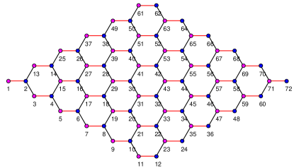
Graphene is a 2D sheet of carbon atoms packed hexagonal structure as depicted in Figure. 1. Since its discoveryNovoselov et al. (2004), graphene has stimulated a tremendous burst of research activities on fundamental and applied grounds. Graphene has multiple astonishing performance in several areas, which is the toughest 2D material ever measured Lee et al. (2008), and also has extremely high charge carriers mobility (charge carriers move at a speed of ( is the speed of light in vacuum)Novoselov et al. (2005); Morozov et al. (2008) and behave like massless particles) More than these, graphene is impermeable to standard gasesBunch et al. (2008) and it could be a perfect thermal conductorBalandin et al. (2008). Numerous other honeycomb liked systems have attracted a lot of attention, such as siliceneVogt et al. (2012), germaneneCahangirov et al. (2009) and phosphoreneLi et al. (2014), which also have excellent properties like graphene. Thus, we expect that these honeycomb like materials will pave the way toward a new age of material.
There is no gap in the band structure of graphene which exhibits semi-metallic propertiesNovoselov et al. (2008); Peres (2010). However, whether the energy gap could be modified in real graphene material to realize the metal-insulator transition (MIT)Drut and Lähde (2009); Schüler et al. (2013); Ulybyshev et al. (2013) is still controversial. If it is possible to control the opening and closing of the energy gap in real graphene, the application of graphene in the electronic device will be greatly promoted.
Recent theoretical and experimental work shows that hydrogenationElias et al. (2009), application of stressNi et al. (2008); Choi et al. (2010); Pletikosić et al. (2009); Meunier et al. (2016); Pereira et al. (2009), forming nanoribbonsHan et al. (2007), Moir-stripe modulationHunt et al. (2013); Ponomarenko et al. (2011), etc. can be used to open the band gap and achieve MIT in graphene. In this work, we explore different approaches to achieving insulating state, considering the interactions between electrons. Graphene is clearly a semimetal without any electron-electron interactions, but it will turn into an insulating antiferromagnet(AFM) under very strong interactionsKotov et al. (2012). However, it still remains unclear as to what we should expect in real graphene materials. For instance, in the real case, it is common to find stress effect in spite of interaction effects, and it is an amazing thing that the electronic properties could be modified by mechanical forcesGui et al. (2015); Aslani et al. (2015); Fanbanrai et al. (2015); Arya et al. (2017); Choi et al. (2009); Cosma et al. (2014); Craco et al. (2015). As for graphene, defects could be introduced naturally or intentionally while growing. The existence of these defects also attract wide interestSummerfield et al. (2016); Zhang et al. (2016). In the experiment, strain could be measured and detected by atomic force microscopy. And strain of on the graphene can be achievedLee et al. (2008), so that the system could completely come into the antiferromagnetic regionLee et al. (2008). Theoretically, there are also a lot of work based on the tight-binding model, studying the effect of uniaxial strain on the properties of graphenePereira et al. (2009). It seems that the gap suddenly arises when deformation is beyond without a transition regionPereira et al. (2009); Choi et al. (2010). To illustrate the strain effect in these heavy fermion materials, the electron interactions should also be considered, and it is interesting to find that the quantum critical point (QCP) strain value is suppressed by interactionsTang et al. (2015). The localization effect and mutual effect of these two factors are the key to understanding the mechanism of MIT in strained graphene. In this paper, we will focus on the competition between electronic correlations and uniaxial strains, and the phase diagram is also discussed.
II Model and numerical method
The Hubbard modelHubbard (1963) is believed to be a versatile paradigm to study strongly correlated electrons on a lattice. It is effective to describe electrons in partially filled energy bands. The parameters of the model, such as hopping and electron-electron interaction, can be considered to be generated by integrating the corresponding degrees of freedom of all energy bands except partially filled narrow bands. Thus, this modelImada et al. (1998) can be used to explain the interaction-driven transition between conducting and insulating behaviors.
To shed light on the physical problems involved in the strained-correlation fermions, we use determinant quantum Monte Carlo (DQMC) to study the half-filled repulsive Hubbard model on the honeycomb lattice. In the Dirac electronic correlation system, it is already known that there exist a QCP for MIT at around Paiva et al. (2005); Sorella et al. (2012); Assaad and Herbut (2013); Arya et al. (2015). In this strength of interaction region, our numerical DQMC method can conduct an accurate simulation. We consider the strained Hubbard Hamiltonian on the honeycomb lattice as
| (1) | |||||
Here () are the spin- electron creation (annihilation) operators at site on sublattice A. And () are operators acting on sublattice B. is the on-site Coulomb repulsion. denotes the hopping integral between two nearest-neighbor sites. The chemical potential determines the average density of the system. and are the number operators. Strain is introduced through the hopping matrix elements along the x-direction which is shown by red lines in Fig. 1. and . Here represents a measure of stress strength. We take as the scale of energy in our system. In this work, we set , thus, the system is half-filled by electrons. And in this case, the Hamiltonian will be particle-hole symmetric even with strain on it, so that the Hamiltonian is sign-problem free to solve in our DQMC simulations.
In the finite-temperature DQMC method, it follows the strategy that take the partition function as an integral over all possible configurations which is carried out by random Monte Carlo sampling. To be more specifically, we can get static and dynamic observables at an given temperature through this approach. As the system is sign-problem free due to the particle-hole symmetry, our calculations can still be in high numerical precision at large enough , thus, we can converge the data to get the ground state. In this work, 4000 sweeps were used to get to the equilibrium state, and 12000 additional steps were made to measure the system. The periodic boundary conditions were used in the simulation, and all the results are obtained on the honeycomb lattice with is large enough to consider the size effect. Fig. 1 shows the geometry with strain on it.
We mainly discussed the MIT in this article. The temperature-dependent DC conductivity is an intuitive physical observation to help characterize the MIT. So that we focus on discussing behavior in our case. According to the fluctuation-dissipation theorem, in the zero frequency limit, is related to the current-current correlation function. As we could do imaginary-time simulations using DQMC, the real-frequency quantities can be easily obtained through analytic continuation methods. In our case, we adopted an approximation Trivedi and Randeria (1995) to define , which has been widely used as a benchmark in previous work Trivedi et al. (1996); Trivedi and Randeria (1995); Denteneer et al. (1999a).
The definition of DC conductivity is:
| (2) |
In Equation (2), is the current-current correlation function, and it can be expressed as , where is the Fourier transform of (time-dependent current operator) along the -direction. When we focus on studying the system in the temperature lower than the energy scale, in which the density of states has a significant structure, the DC conductivity definition, in Equation(2), can be very practicable considering such approximation. The applicability has been checked in our recent work of the Hubbard model on the honeycomb latticeMa et al. (2018). We can get the MIT critical strength value Denteneer et al. (1999b) within the formula from the change of low- behavior of . We also investigate the magnetic properties by carrying out measurements of spin-spin correlation functions and the spin structure factor,
| (3) |
where is the number of sites in the lattice, and and represents the sublattices of the honeycomb lattice. Here is the component spin operator. The results are normalized by including all the lattice sites. The antiferromagnetic results present in this work are concluded from the constrained-path quantum Monte Carlo (CPQMC) methodZhang et al. (1997, 1995); Ma et al. (2011), which uses the constrained-path approximation in the simulation procedure without a sign problem.

III Results and discussion
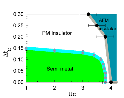
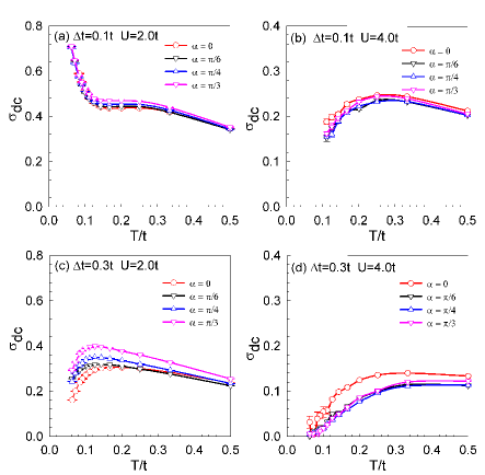
Our simulations are mainly computed on the lattice considering the size effect. is the total site numbers. The quantity of immediate interest in this work is to study the possible MIT of the strained honeycomb lattice, which can be measured by the and its dependence behavior. So we show the behavior at low temperature here in Figure. 3. For some curves, and diverges as decreases to the limit, which suggesting metallic behavior of the system. In contrast, the system is insulating when at limit. Thus, we can easily tell the MIT point of the strained system. In panels (a)-(b) of Fig. 3, we described behaviors at low coupling strengths under several strain strengths. To understand the role of strain on the conductivity, we can take a careful analyzation of panel (a) in Fig. 3. In spite of strength, the conductivity increases as temperature increases until . However when and with a strong enough strain strength , the curve bent down when temperature drops and approaches zero as , suggesting insulating behavior of the system. In contrast, when we take a look at , the red line diverges with feature of for , characteristic the metallic behavior of the system. Thus, we can clearly get the strain-driven MIT critical point from the panels. At , the critical value can be read as . As for panel (b) in Fig. 3 with . At , curve is concave and for . When drops to around , increases rapidly, in other words, the system is metallic. At , in contrast, the conductivity decreases as the temperature decreases, which indicating insulating behaviors. Thus, there exist a MIT critical strain strength at around for on the graphene lattice. Then it moves to the larger interaction case, as shoen in Fig. 3(c) and (d). When , the system is still metallic without considering strain effect. So that under small strain strength, it is still possible that the graphene can stay in metallic region. At low for , the sign of is negative when , but it switches to positive when is larger than . Therefore, the MIT critical strengths can be read as for . As for which is larger than the critical for MIT in the graphene lattice without strain, the system is an insulator. From panel (d), we can see all the curves are bent down when temperature decreased for . The value of gets suppressed when strength of strain increases, that is to say the insulating behavior is preserved by the strain effect in this case. To describe the metal-insulator phase boundary more precisely, we closely studied the conductivity behaviour around . Thus, according to Fig. 6 in Appendix, we make the metal-insulator phase boundary more smooth, as shown in the phase diagram Fig. 2.
In Fig. 4, we also investigate the effect of the orientation of the strain. Here in each panel is the angle with x-axis. Panel (a) is in the metallic regime for and . As increases to , the system turns into the insulating regime, as panel (c) shows. Comparing panel (b) and (d), the result at is shown that graphene stays in the insulating state no matter how strong the strain applied. According to the lines in Fig. 4, it seems that the behavior of is pretty similar when changes. We only consider the nearest hopping in our Hamiltonian, which is a single-shell model. The shell behavior to the angles is very similar to the first shell of the model including up to third-nearest-neighbor interactionsBotello-Méndez et al. (2018). The angular dependence is not very important considering atoms in the second and third shells, thus, we get the similar behaviors of here with different orientations of strain. Therefore, we can focus our study on the strength of strain and ignore its orientation when exploring the strain effect on MIT.
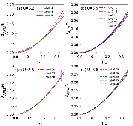
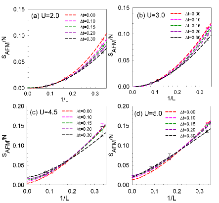
Further more, we also studied the effect of strain on long-range magnetic order. Data shown in Fig. 5 and Fig. 7 are AF spin structure factor on lattices up to . For small , there is no long-range order when Paiva et al. (2005); Sorella et al. (2012); Assaad and Herbut (2013); Arya et al. (2015). Even when , there is no AF order according to Fig. 7(a) and (b). As for small lattices, the correlation strength of antiferromagnetism decreases while strain increases, which indicates that in the weak interaction case, are suppressed by strain. In contrast, in Fig. 7(c) and (d), AF correlation strength is enhanced by strain at large . The AF order is protected by strain at strong interaction (). As Fig. 5 shows, it is interesting to note that the AF order could exist even when . Thus, there is a transition point that exists for long-range order by strain effect. We obtained (a), (b),(a) and (a) from the finite size scaling results. Based on the analysis earlier, the paramagnetic-antiferromagnetic transition boundary could be summarised for nonzero , as shown in Fig. 2.
IV Summary
We have carefully studied the electronic and magnetic properties of the strained Hubbard model on the honeycomb lattice. Using DQMC, we characterize the with the behavior at low temperature to explore the mechanism of strain-driven MIT in the honeycomb lattice. According to our simulations, it is clear to see that the conductivity is suppressed by strain effect. When strain is applied, the value of hopping parameter along the strain direction decreases from to , thus, the critical electron-electron interaction strength for MIT reduces. And the critical strain strength decreases as the local Coulomb repulsion enhanced. In other words, under the interaction of strain and Coulomb correlation, the electrons get localized more effectively, which expands the insulating phase and gives us a strain-interaction driven MIT phase diagram.
As for the magnetic properties, we found that strain could also enhance the AF order at around in the clean limit. While strain is affected, we observed the appearance of the antiferromagnetic order phase. It seems that strain can protect the long antiferromagnetic order when is strong. In conclusion, we show that strain-interaction-driven graphene could be a promising rout to achieve MIT in graphene, and the phase diagram reported in this work could be used as a guidance in the modulation of conductivity in real graphene materials.
T. M. and L. F. Z were supported by NSFCs (No. 11774033 and 11974049) and Beijing Natural Science Foundation (No. 1192011).
References
- Novoselov et al. (2004) K. S. Novoselov, A. K. Geim, S. V. Morozov, D. Jiang, Y. Zhang, S. V. Dubonos, I. V. Grigorieva, and A. A. Firsov, Science 306, 666 (2004).
- Lee et al. (2008) C. Lee, X. Wei, J. W. Kysar, and J. Hone, Science 321, 385 (2008).
- Novoselov et al. (2005) K. S. Novoselov, A. K. Geim, S. V. Morozov, M. I. Jiang, D.and Katsnelson, I. V. Grigorieva, S. V. Dubonos, and A. A. Firsov, Nature 438, 197 (2005).
- Morozov et al. (2008) S. V. Morozov, K. S. Novoselov, M. I. Katsnelson, F. Schedin, D. C. Elias, J. A. Jaszczak, and A. K. Geim, Phys. Rev. Lett. 100, 016602 (2008).
- Bunch et al. (2008) J. S. Bunch, S. S. Verbridge, J. S. Alden, A. M. Van, der Zande, J. M. Parpia, H. G. Craighead, and P. L. Mceuen, Nano Letters 8, 2458 (2008).
- Balandin et al. (2008) A. A. Balandin, S. Ghosh, W. Bao, I. Calizo, D. Teweldebrhan, F. Miao, and C. N. Lau, Nano Letters 8, 902 (2008).
- Vogt et al. (2012) P. Vogt, P. De Padova, C. Quaresima, J. Avila, E. Frantzeskakis, M. C. Asensio, A. Resta, B. Ealet, and G. Le Lay, Phys. Rev. Lett. 108, 155501 (2012).
- Cahangirov et al. (2009) S. Cahangirov, M. Topsakal, E. Aktürk, H. Şahin, and S. Ciraci, Phys. Rev. Lett. 102, 236804 (2009).
- Li et al. (2014) L. Li, Y. Yu, G. Ye, Q. Ge, X. Ou, H. Wu, D. Feng, X. Chen, and Y. Zhang, Nature Nanotechnology 9, 372 (2014).
- Novoselov et al. (2008) K. Novoselov, P. Blake, and M. Katsnelson, in Encyclopedia of Materials: Science and Technology, edited by K. J. Buschow, R. W. Cahn, M. C. Flemings, B. Ilschner, E. J. Kramer, S. Mahajan, and P. Veyssière (Elsevier, Oxford, 2008) pp. 1 – 6.
- Peres (2010) N. M. R. Peres, Physica Status Solidi 244, 4106 (2010).
- Drut and Lähde (2009) J. E. Drut and T. A. Lähde, Phys. Rev. Lett. 102, 026802 (2009).
- Schüler et al. (2013) M. Schüler, M. Rösner, T. O. Wehling, A. I. Lichtenstein, and M. I. Katsnelson, Phys. Rev. Lett. 111, 036601 (2013).
- Ulybyshev et al. (2013) M. V. Ulybyshev, P. V. Buividovich, M. I. Katsnelson, and M. I. Polikarpov, Phys. Rev. Lett. 111, 056801 (2013).
- Elias et al. (2009) D. C. Elias, R. R. Nair, T. M. G. Mohiuddin, S. V. Morozov, P. Blake, M. P. Halsall, A. C. Ferrari, D. W. Boukhvalov, M. I. Katsnelson, A. K. Geim, and K. S. Novoselov, Science 323, 610 (2009).
- Ni et al. (2008) Z. H. Ni, T. Yu, Y. H. Lu, Y. Y. Wang, Y. P. Feng, and Z. X. Shen, ACS Nano 2, 2301 (2008), pMID: 19206396.
- Choi et al. (2010) S.-M. Choi, S.-H. Jhi, and Y.-W. Son, Phys. Rev. B 81, 081407 (2010).
- Pletikosić et al. (2009) I. Pletikosić, M. Kralj, P. Pervan, R. Brako, J. Coraux, A. T. N’Diaye, C. Busse, and T. Michely, Phys. Rev. Lett. 102, 056808 (2009).
- Meunier et al. (2016) V. Meunier, A. G. Souza Filho, E. B. Barros, and M. S. Dresselhaus, Rev. Mod. Phys. 88, 025005 (2016).
- Pereira et al. (2009) V. M. Pereira, A. H. Castro Neto, and N. M. R. Peres, Phys. Rev. B 80, 045401 (2009).
- Han et al. (2007) M. Y. Han, B. Özyilmaz, Y. Zhang, and P. Kim, Phys. Rev. Lett. 98, 206805 (2007).
- Hunt et al. (2013) B. Hunt, J. D. Sanchez-Yamagishi, A. F. Young, M. Yankowitz, B. J. LeRoy, K. Watanabe, T. Taniguchi, P. Moon, M. Koshino, P. Jarillo-Herrero, and R. C. Ashoori, Science 340, 1427 (2013).
- Ponomarenko et al. (2011) L. A. Ponomarenko, A. K. Geim, A. A. Zhukov, R. Jalil, S. V. Morozov, K. S. Novoselov, I. V. Grigorieva, E. H. Hill, V. V. Cheianov, and V. I. Fal’Ko, Nature Physics 7, 958 (2011).
- Kotov et al. (2012) V. N. Kotov, B. Uchoa, V. M. Pereira, F. Guinea, and A. H. Castro Neto, Rev. Mod. Phys. 84, 1067 (2012).
- Gui et al. (2015) G. Gui, D. Morgan, J. Booske, J. Zhong, and Z. Ma, Applied Physics Letters 106, 666 (2015).
- Aslani et al. (2015) M. Aslani, C. M. Garner, S. Kumar, D. Nordlund, P. Pianetta, and Y. Nishi, Applied Physics Letters 81, 720 (2015).
- Fanbanrai et al. (2015) P. Fanbanrai, A. Hutem, and S. Boonchui, Physica B Condensed Matter 472, 84 (2015).
- Arya et al. (2017) S. Arya, M. S. Laad, and S. R. Hassan, Phys. Rev. B 96, 085126 (2017).
- Choi et al. (2009) S. M. Choi, S. H. Jhi, and Y. W. Son, Physical Review B Condensed Matter 81, 081407(R) (2009).
- Cosma et al. (2014) D. A. Cosma, M. Mucha-Kruczyński, H. Schomerus, and V. I. Fal’ko, Phys. Rev. B 90, 245409 (2014).
- Craco et al. (2015) L. Craco, D. Selli, G. Seifert, and S. Leoni, Physical Review B 91 (2015).
- Summerfield et al. (2016) A. Summerfield, A. Davies, T. S. Cheng, V. V. Korolkov, J. C. Yong, C. J. Mellor, C. T. Foxon, A. N. Khlobystov, K. Watanabe, and T. Taniguchi, Sci Rep 6, 22440 (2016).
- Zhang et al. (2016) W. Zhang, W. C. Lu, H. X. Zhang, K. M. Ho, and C. Z. Wang, Carbon 110, 330 (2016).
- Tang et al. (2015) H.-K. Tang, E. Laksono, J. N. B. Rodrigues, P. Sengupta, F. F. Assaad, and S. Adam, Phys. Rev. Lett. 115, 186602 (2015).
- Hubbard (1963) J. Hubbard, Proceedings of the Royal Society of London. Series A. Mathematical and Physical Sciences 276, 238 (1963).
- Imada et al. (1998) M. Imada, A. Fujimori, and Y. Tokura, Rev. Mod. Phys. 70, 1039 (1998).
- Paiva et al. (2005) T. Paiva, R. T. Scalettar, W. Zheng, R. R. P. Singh, and J. Oitmaa, Phys. Rev. B 72, 085123 (2005).
- Sorella et al. (2012) S. Sorella, Y. Otsuka, and S. Yunoki, Scientific Reports 2, 992 (2012).
- Assaad and Herbut (2013) F. F. Assaad and I. F. Herbut, Phys. Rev. X 3, 031010 (2013).
- Arya et al. (2015) S. Arya, P. V. Sriluckshmy, S. R. Hassan, and A.-M. S. Tremblay, Phys. Rev. B 92, 045111 (2015).
- Trivedi and Randeria (1995) N. Trivedi and M. Randeria, Phys. Rev. Lett. 75, 312 (1995).
- Trivedi et al. (1996) N. Trivedi, R. T. Scalettar, and M. Randeria, Phys. Rev. B 54, R3756 (1996).
- Denteneer et al. (1999a) P. J. H. Denteneer, R. T. Scalettar, and N. Trivedi, Phys. Rev. Lett. 83, 4610 (1999a).
- Ma et al. (2018) T. Ma, L. Zhang, C.-C. Chang, H.-H. Hung, and R. T. Scalettar, Phys. Rev. Lett. 120, 116601 (2018).
- Denteneer et al. (1999b) P. J. H. Denteneer, R. T. Scalettar, and N. Trivedi, Phys. Rev. Lett. 83, 4610 (1999b).
- Zhang et al. (1997) S. Zhang, J. Carlson, and J. E. Gubernatis, Phys. Rev. Lett. 78, 4486 (1997).
- Zhang et al. (1995) S. Zhang, J. Carlson, and J. E. Gubernatis, Phys. Rev. Lett. 74, 3652 (1995).
- Ma et al. (2011) T. Ma, Z. Huang, F. Hu, and H.-Q. Lin, Phys. Rev. B 84, 121410 (2011).
- Botello-Méndez et al. (2018) A. R. Botello-Méndez, J. C. Obeso-Jureidini, and G. G. Naumis, The Journal of Physical Chemistry C 122, 15753 (2018).
.1 Computing the DC conductivity
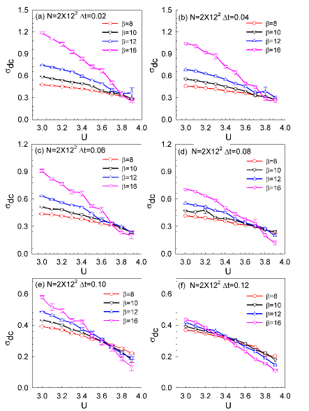
In this work, the low-temperature behavior of DC conductivity is used to distinguish metallic or insulating phases. We found that the transition point changes dramatically at around . So in appendix Fig. 6, we carefully checked the phase boundary by plotting the curves, which indicate a critical transition strength in each panel. While in panel (a), when , gradually increases as get larger, which indicates the metallic behavior. On the other side, when , decreases as increases, which act as an insulator. Thus, the critical transition point for is . And other transition points are (b) ,,(c) ,,(d) ,,(e) , and (f) ,.
.2 Existence of the AF order phase
To establish the phase diagram, the finite-size effect on the AF spin structure factor has been carefully examined in the manuscript. We extrapolated the data to the thermodynamic limit to get the order parameters. As shown in Fig . 7, we discussed the strain effect on the honeycomb lattice with various interaction strengths. All the results are summarized in the phase diagram Fig . 2.