How high is a MoSe2 monolayer?
Abstract
Transition metal dichalcogenides (TMDCs) have attracted significant attention for optoelectronic, photovoltaic and photoelectrochemical applications. The properties of TMDCs are highly dependent on the number of stacked atomic layers, which is usually counted post-fabrication, using a combination of optical methods and atomic force microscopy (AFM) height measurements. Here, we use photoluminescence spectroscopy and three different AFM methods to demonstrate significant discrepancies in height measurements of exfoliated MoSe2 flakes on SiO2 depending on the method used. We highlight that overlooking effects from electrostatic forces, contaminants and surface binding can be misleading when measuring the height of a MoSe2 flake. These factors must be taken into account as a part of the protocol for counting TMDC layers.
Keywords: Molybdenum Diselenide (MoSe2), Transition Metal Dichalcogenides (TMDCs), 2D materials, atomic force microscopy (AFM), photoluminescence spectroscopy (PL), mechanical exfoliation
1 Introduction
Transition metal dichalcogenides (TMDCs) are of increasing interest as promising contenders for a wide range of optoelectronic and electrochemical applications due to their strong light-matter interactions, tunable optical bandgaps and flexible two-dimensional (2D) structure [1, 2]. Molybdenum diselenide (MoSe2) is one of the most promising TMDC candidates for photoelectrochemical energy conversion due to its photocatalytic properties and the electrical conductivity of Se [3, 1]. MoSe2 monolayers have a hexagonal crystal structure that consists of top and bottom Se layers sandwiching a Mo layer [4]. Stacked MoSe2 layers are weakly coupled via van der Waals coupling[5] and have an interlayer spacing in bulk of 0.65 nm[6, 7, 8, 9, 10].
The number of stacked atomic layers in TMDC samples can drastically affect their properties [11, 12, 4]. For example, a MoSe2 monolayer has a direct bandgap of 1.55 eV (800 nm) [13], which transitions to an indirect bandgap as the number of layers increases to 2 and 3 [13, 14, 15, 5]. For both fundamental studies and device functionality, it is therefore vital to be able to confirm the number of layers present in TMDC samples. In addition, it is important to understand how the properties of the different layers in stacked TMDC structures could be influenced during fabrication and from interactions with the underlying substrate [16].
As with other 2D materials, TMDC layers can be synthesized both via chemical vapor deposition (CVD) [17, 18, 19] and, most commonly, using mechanical exfoliation [16, 11, 1, 2, 20, 21, 22, 14], in which mono- or few-layer flakes are transferred onto a substrate, often SiO2/Si. Studies of factors from the fabrication process influencing the measured step heights and optical properties of monolayers have been emerging mostly on MoS2 [20, 23], whereas the literature for other TMDCs such as MoSe2 is limited in comparison. E. Pollman et al. [16] carried out a study on MoS2 comparing the properties of samples fabricated from both techniques, and showed that a major difference is the presence of intercalated water on exfoliated monolayers, leading to both an increased step height and a decreased intensity in photoluminescence spectroscopy [16]. A further challenge is that samples are often handled in air, leading to airborn contaminants [24]. Interestingly, MoSe2 has been shown to be even more susceptible to surface contaminants than sulfur-based TMDCs [24], so understanding how contaminants and other effects may influence the height (and thus layer number) measurements for MoSe2 is highly relevant.
1.1 Methods for counting layers
The number of layers present in TMDC samples is usually measured using a combination of optical microscopy [25, 26], photoluminescence spectroscopy (PL) and/or Raman spectroscopy together with step height measurements made by atomic force microscopy (AFM) [15, 27, 17, 28]. In optical microscopy images, the contrast difference between layers can be analysed for the red, green and blue channels of the image [29, 12, 30]. AFM is used to measure the height of a flake, and comparing that to the expected interlayer spacing of the 2D material. There is much discrepancy among AFM height measurements of mechanically exfoliated TMDCs on SiO2: Some show heights between 0.65 - 1.0 nm[22, 14, 27] while others are much larger, ranging between 2 - 3 nm [20, 31]. Elevated heights are often attributed to surface contaminants [20, 14, 1, 32].
PL is another widely used technique used to characterize TMDC layer numbers. The position of the monolayer peak in a PL spectrum for exfoliated MoSe2 samples has been observed at room temperature in the range 788 - 816 nm [14, 15, 33, 34, 5, 35, 17, 18]. The PL intensity can be a affected by the presence of defects [19] and adsorbates [15] and is expected to decrease as the number of layers increases to 2 and 3 [13, 14, 15, 5]. There is a lack of consensus in the literature regarding how to interpret PL spectra for 2, 3, and N layers of MoSe2. For MoSe2 flakes mechanically exfoliated onto SiO2/SiO, P. Tonndorf et al. [15] show a 15 nm redshift of the dominant A peak for a bilayer and significant broadening and flattening of the A peak for 3 layers. In contrast, Y. Sha et al. [14] measured only a few nm redshift as the number of MoSe2 layers increases. S. Tongay et al. [13] also show a negligible shift in position of the peak as the number of MoSe2 layers increases from 1 to 3 layers. In some cases, observations from bilayers have exhibited the properties of a monolayer, which is thought to be due to the formation of pockets between the layers during exfoliation[27]. The degree of coupling between exfoliated MoSe2 layers has been shown to significantly influence their photoluminescence, as demonstrated by S. Tongay et al. using thermally controlled coupling [13].
In this work, two MoSe2 flakes were measured using optical microscopy, PL spectroscopy and three different modes of AFM: tapping mode, non-contact AFM (nc-AFM) and Kelvin probe force microscopy (KPFM). The presence of electrostatic forces can significantly influence the topographic height profile measured using nc-AFM [36, 37]. In KPFM, the net electrostatic force is minimized using a feedback loop to apply a DC bias, and KPFM thereby provides information about contact potential variations over the sample surface, either due to nonhomogeneities in the sample material or localized charging or polarization effects.
2 Results & Discussion
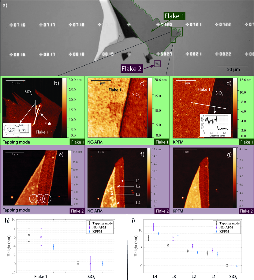
MoSe2 flakes were transferred onto a substrate of SiO2 using all-dry viscoelastic stamping [25]. Figure 1 provides an overview of the sample regions that were selected for study. Flake 1 is the largest, most visibly transparent area of the sample, and Flake 2 is a small island that has stepped layers. Figure 1a shows a grayscale image of the red channel of the R, G, B channels of the color optical image (the red channel is selected here as it shows the highest degree of contrast between the layers). Figures 1b-d and 1e-g show tapping mode, nc-AFM, and KPFM z-channel images of Flake 1 and Flake 2 respectively. The data in the KPFM z-channel images is the z-height measured after compensating for the contribution of the net electrostatic force to the height data.
In the nc-AFM scan in Figure 1f, Flake 2 appears to be stepped, with an overlayer of some additional features on the top layer. The apparent stepped layers and overlayer have been labeled L1, L2, L3, and L4 (note that these regions do not necessarily correspond to 1, 2, 3, and 4 atomic layers). Figures 1h-i show the height measurements extracted from the AFM images, which are presented in tabular form in the Supplementary Materials.
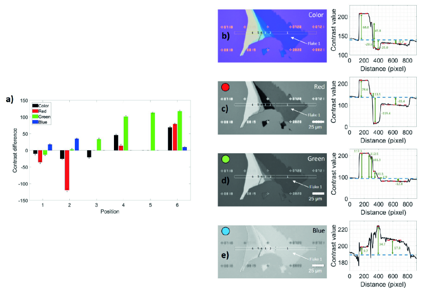
Comparing the optical contrast difference between Flake 1 and the substrate (values given for the color, green and blue channels in Supplementary Materials) for both the color image and red channel image to observations of other TMDCs (MoS2 and WSe2) on 300 nm SiO2/Si [38], the contrast of Flake 1 agrees with that of a monolayer rather than two stacked layers. However, a definite determination of the layer count based on optical contrast is difficult for a sample that is not consisting of large flakes of 1, 2, 3, …, N layers, where the transmittances from each flake can be compared relative to each other [29]. L. Ottaviano et al [20] demonstrated for MoS2, that optical microscopy data alone can be misleading, as the contrast depends on the exact thickness of the SiO2 layer on Si/SiO2 samples, and is not always a monotonic function of the layer number [20]. Optical microscopy could not be used to reliably characterize Flake 2 because it has dimensions smaller than the diffraction limit of light - another limitation of determining layer number by optical contrast [20].
2.1 AFM
The apparent AFM heights, shown in Figures 1h-i, were measured by averaging large areas of the AFM images shown in Figures 1b-g. Area averaging provides more robust, quantitative height measurements than individual line scans. See the Supplementary Materials for more information as well as the results of Figure 1h-i presented in tabular form. Figures 1h-i show that the height measurements of each AFM mode - tapping, nc-AFM and KPFM - often do not agree within uncertainty. This is because each mode provides different information about the sample properties, such as mechanical rigidity and electrostatic nonuniformity. For example, the step height between the substrate and Flake 1 in the KPFM scan (3.9 0.8 nm) is significantly smaller than in the tapping mode and nc-AFM scans, suggesting that electrostatic forces inflate the height measurements when they are not compensated for. Similarly, the systematically lower heights measured with tapping mode on Flake 2 could be explained by mechanical compression of an overlayer or underlayer, since tapping mode is operated in a larger tip-sample force regime than nc-AFM and KPFM, so it is much more likely to mechanically influence (e.g. compress) the sample.
For each AFM mode, the substrate:Flake 1 and substrate:L1 heights measured with each AFM technique are all substantially higher than the nm expected for a single layer of MoSe2. This result is similar to observations by L. Ottaviano et al.[20]. Notably, the surface roughness of the sample measured with each AFM mode is also much larger than the atomic-scale roughness expected for clean MoSe2 flakes. The line scan in the inset of Figure 1d shows an example of the surface roughness: On the SiO2 substrate, the roughness is sub-nanometer, whereas on Flake 1 the roughness is greater than 2 nm. Roughness characterizations of each AFM mode, shown in the Supplementary Materials, yield similar results. This suggests that the sample has a rough overlayer or underlayer, or is highly defective. Such a layer may have been left behind during sample fabrication.
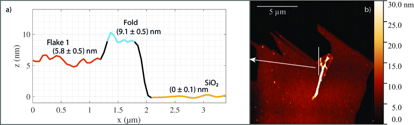
At the location where Flake 1 is folded, shown in the tapping mode data in Figure 1b, the step height between Flake 1 and the fold is smaller than the step between the SiO2 substrate and Flake 1, as indicated by the line trace in the inset. Note that the height of the fold could not be accurately determined using the area averaging method, since the fold is too small. The height measurements from the line trace only are shown in Supplementary Materials. However, this difference in step height could further indicate the presence of an underlayer between the bottom layer and the substrate which is not present between stacked layers.
The most notable electrostatic feature is L4 on Flake 2, shown in Figure 1f-g: With nc-AFM, L4 is several nanometers high, whereas with KPFM compensation L4 is indistinguishable within the surface roughness from L3. The features comprising L4, which could be either on top of or underneath Flake 2, remained unchanged in shape and location even after the sample was annealed several times at 130 ∘C in UHV for eight hours. L4 could be surface contamination introduced during the sample fabrication procedure: Selenium-based TMDCs that have been mechanically exfoliated under ambient conditions have been shown to be highly susceptible to airborne contaminants which are mobile on the surface and aggregate to larger patches with average height of 2.2 nm over 45 hours, influencing the apparent monolayer height and interlayer spacing[24].
Another notable feature shown in Figures 1f-g is that the apparent step height between L1 and L2 in the nc-AFM image becomes zero within error when electrostatic forces are compensated with KPFM. E. Pollmann et al. showed for MoS2 that the degree of screening of charge transfer to the SiO2 substrate can depend on variation in water layers lying underneath the surface. The large uncertainty due to the roughness prevents a clear determination of whether an atomic step is present, but this result shows that non-uniform charging alone (e.g. due to variation in underlying water layers) can also simulate the presence of a step, and must be compensated for.
2.2 Photoluminescence data
The results of characterization using PL spectroscopy of Flake 1 and Flake 2 are shown in Figure 2. The signal measured at the center of Flake 1 (Figure 2a, blue) is no greater than the SiO2 background signal. This could be due to the presence of a water film between the SiO2 and MoSe2; Similar PL signal quenching has been observed for exfoliated MoS2 monolayers, and it was determined to be caused by intercalated water between the substrate and the MoS2 [16, 39]. Previously reported weak PL intensities[40, 13], or peak broadening have also been thought to be caused by aging effects such as oxidation and contamination of adsorbates [41]. A high intensity peak (Figure 2a, green) was detected at the corner of Flake 1 where a fold is visible in Figures 1a and b. The PL peak from this fold lies at a wavelength of 798 2 nm. This agrees with the predicted position, peak shape and linewidth that have been reported for both a monolayer[15, 13] and a bilayer data[14]. Depending on the degree of coupling with the underlying layer [42, 13], the fold could be behaving as a suspended monolayer with contributions from a bilayer signal.
The dominant peak at 800 nm is the A-exciton (ground state exciton) contribution[33, 17], and a second smaller peak is present at 91 nm below (i.e. at 200 meV higher energy), which corresponds to the B-exciton (higher spin-orbit split state). The ratio of the intensities of the A and B peak is linked to the number of defects in the sample, where a higher B/A ratio indicates higher defect density [33]. Fitting the data from the fold in Figure 2a with the sum of two Lorentzian peaks, we obtain the results shown in the inset. The B/A ratio is 0.04, suggesting a relatively high defect density compared to the values measured by K. McCreary et al. [33], where the highest B/A ratio observed for MoSe2 monolayers synthesized by CVD was 0.025.
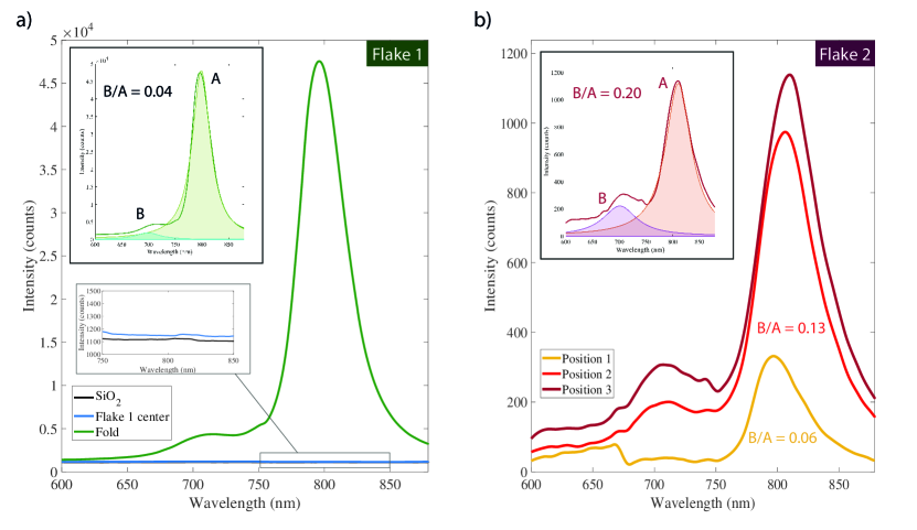
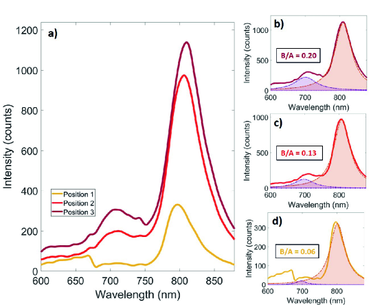
The PL spectra acquired at three positions on Flake 2 are shown in Figure 2b. The approximate position of the center of the laser beam corresponding to these three positions are labelled in Figure 1e. Since the laser beam area was larger than the individual steps in the flake, the measured peaks are expected to be a convolution of contributions from the different layers. The spectrum at position 1 (yellow) has the A peak at (801 3) nm, in agreement with the peak position of the fold in Figure 2a, and hence of a monolayer as observed in [15, 13]. As the spot moves over the island from right to left, the peak position shifts towards 810 nm, as expected for an increasing number of layers [15, 18, 14]. The B/A ratio increases as the number of layers increases from right to left, and the top layer has a very high ratio of 0.20. Here, we do not see the intensity decreasing as the number of layers increases. This could be due to decoupling of the layers [27], but is also likely influenced by the fact that the laser beam spot is large and hence also partly covers the SiO2 in for example the measurement at position 1, and hence sees a smaller contribution from MoSe2. The results demonstrate how the presence of water and/or defects that are not visible optically can affect the PL peaks, highlighting the importance of thorough spatial characterization at the nm-scale in order to uncover the quality of the sample.
3 Conclusion
MoSe2 flakes transferred onto SiO2 were characterized using optical microscopy, PL spectroscopy and three modes of AFM. We showed complete quenching of the photoluminescence peak on the large Flake 1, which may be caused by an underlayer of water or other contamination. Electrostatic nonhomogeneities, a large uniform surface roughness and mechanical compressibility of the sample all indicate the presence of an over- or underlayer, which would also explain higher-than-expected layer heights measured in AFM. We have shown that the height of MoSe2 layers on SiO2 depends on the condition of the sample, and that it is vital to interpret step heights measured using AFM methods correctly.
The approach typically used to count the number of layers in a TMDC sample is to combine an optical measurement with AFM data. Here we have demonstrated that great care must be taken when using these methods, as the layer count can be difficult to deconvolute from effects of charging, defects and contaminants, and any one method alone can lead to an incorrect or incomplete characterization of the sample.
4 Methods
MoSe2 layers were exfoliated onto SiO2 using all-dry viscoelastic stamping. This process uses mechanical exfoliation to transfer 2D crystals onto a viscoelastic Gelfilm stamp, which in turn is pressed against the desired substrate to transfer the flakes onto the surface [25]. Optical microscopy images were obtained using a Nikon optical microscope (Nikon Eclipse LV150N) in reflective mode with a 50x times magnification objective.
Tapping mode measurements were performed in air with a MFP3D (BIO) Asylum microscopy using 240C-PP OPUS tips with 1-2 N/m spring constant and oscillation amplitudes between 14-16 nm. Nc-AFM and KPFM measuremens were performed in ultrahigh vacuum after having been annealed at 130∘C for 8 hours with a modified JEOL JSPM-4500A UHV surface science system at room temperature, using Nanosensors platinum-iridium coated silicon tips with resonant frequency 330 kHz and spring constant 42 N/m.
Photoluminescence spectra were collected at room temperature using a 532 nm laser excitation with a power of 150 µW and 30 s exposure time. A 100X objective was used to focus the laser beam on the sample. The spot size diameter was approximately 1 µm.
Acknowledgments
The authors thank Philipp Nagler for the fabrication of the MoSe2 sample and the acquisition of the optical microscopy image at Universität Regensburg. Funding from NSERC and FRQ-NT are gratefully acknowledged.
References
References
- [1] Changli Li, Qi Cao, Faze Wang, Yequan Xiao, Yanbo Li, Jean Jacques Delaunay, and Hongwei Zhu. Engineering graphene and TMDs based van der Waals heterostructures for photovoltaic and photoelectrochemical solar energy conversion. Chem. Soc. Rev., 47:4981–5037, 2018.
- [2] Sonali Das, Deepak Pandey, Jayan Thomas, and Tania Roy. The Role of Graphene and Other 2D Materials in Solar Photovoltaics. Adv. Mater., 31:1802722, 2019.
- [3] Ali Eftekhari. Molybdenum diselenide (MoSe2) for energy storage, catalysis, and optoelectronics. Applied Materials Today, 8:1–17, 2017.
- [4] Qing Hua Wang, Kourosh Kalantar-Zadeh, Andras Kis, Jonathan N. Coleman, and Michael S. Strano. Electronics and optoelectronics of two-dimensional transition metal dichalcogenides. Nature Nanotech., 7:699–712, 2012.
- [5] Chinh Tam Le, Daniel J. Clark, Farman Ullah, Velusamy Senthilkumar, Joon I. Jang, Yumin Sim, Maeng Je Seong, Koo Hyun Chung, Hyoyeol Park, and Yong Soo Kim. Nonlinear optical characteristics of monolayer MoSe2. Ann. Phys., 528:1–9, 2016.
- [6] P. B. James and M. T. Lavik. The crystal structure of MoSe2. Acta Cryst., 16:1183, 1963.
- [7] Y. Tomm and S. Fiechter. Crystal growth of materials for photovoltaics. Journal of Ceramic Processing Research, 6:141–145, 2005.
- [8] S. K. Mahatha, K. D. Patel, and Krishnakumar S.R. Menon. Electronic structure investigation of MoS2 and MoSe2 using angle-resolved photoemission spectroscopy and abinitio band structure studies. J. Phys.: Condens. Matter, 24:475504, 2012.
- [9] Anupam Roy, Hema C.P. Movva, Biswarup Satpati, Kyounghwan Kim, Rik Dey, Amritesh Rai, Tanmoy Pramanik, Samaresh Guchhait, Emanuel Tutuc, and Sanjay K. Banerjee. Structural and Electrical Properties of MoTe2 and MoSe2 Grown by Molecular Beam Epitaxy. ACS Appl. Mater. Interfaces, 8:7396–7402, 2016.
- [10] Fan Jiang, Wen-Sheng Zhao, and Jun Zhang. Mini-review: Recent progress in the development of MoSe2 based chemical sensors and biosensors. Microelectronic Engineering, 225:111279, 2020.
- [11] Wonbong Choi, Nitin Choudhary, Gang Hee Han, Juhong Park, Deji Akinwande, and Young Hee Lee. Recent development of two-dimensional transition metal dichalcogenides and their applications. Materials Today, 20:116–130, 2017.
- [12] Hao Zhang, Feirong Ran, Xiaotong Shi, Xiangru Fang, Shiyu Wu, Yue Liu, Xianqiang Zheng, Peng Yang, Yang Liu, Lin Wang, Xiao Huang, Hai Li, and Wei Huang. Optical thickness identification of transition metal dichalcogenide nanosheets on transparent substrates. Nanotechnology, 28:164001, 2017.
- [13] Sefaattin Tongay, Jian Zhou, Can Ataca, Kelvin Lo, Tyler S. Matthews, Jingbo Li, Jeffrey C. Grossman, and Junqiao Wu. Thermally Driven Crossover from Indirect toward Direct Bandgap in 2D Semiconductors: MoSe2 versus MoS2. Nano Lett., 12:5576–5580, 2012.
- [14] Yunfei Sha, Shaoqing Xiao, Xiumei Zhang, Fang Qin, and Xiaofeng Gu. Layer-by-layer thinning of MoSe2 by soft and reactive plasma etching. Applied Surface Science, 411:182–188, 2017.
- [15] Philipp Tonndorf, Robert Schmidt, Philipp Böttger, Xiao Zhang, Janna Börner, Andreas Liebig, Manfred Albrecht, Christian Kloc, Ovidiu Gordan, Dietrich R. T. Zahn, Steffen Michaelis de Vasconcellos, and Rudolf Bratschitsch. Photoluminescence emission and Raman response of monolayer MoS2, MoSe2, and WSe2. Opt. Express, 21:4908–4916, 2013.
- [16] Erik Pollmann, Lukas Madauß, Simon Schumacher, Uttam Kumar, Flemming Heuvel, Christina vom Ende, Sümeyra Yilmaz, Sümeyra Güngörmüs, and Marika Schleberger. Apparent differences between single layer molybdenum disulphide fabricated via chemical vapour deposition and exfoliation. Nanotechnology, 31:15505604, 2020.
- [17] Xin Lu, M. Iqbal Bakti Utama, Junhao Lin, Xue Gong, Jun Zhang, Yanyuan Zhao, Sokrates T. Pantelides, Jingxian Wang, Zhili Dong, Zheng Liu, Wu Zhou, and Qihua Xiong. Large-area synthesis of monolayer and few-layer MoSe2 films on SiO2 substrates. Nano Lett., 14:2419–2425, 2014.
- [18] Siyuan Wang, Guang Wang, Xi Yang, Hang Yang, Mengjian Zhu, Sen Zhang, Gang Peng, and Zheng Li. Synthesis of Monolayer MoSe2 with Controlled Nucleation via Reverse-Flow Chemical Vapor Deposition. Nanomaterials, 10:75, 2019.
- [19] Xingli Wang, Yongji Gong, Gang Shi, Wai Leong Chow, Kunttal Keyshar, Gonglan Ye, Robert Vajtai, Jun Lou, Zheng Liu, Emilie Ringe, Beng Kang Tay, and Pulickel M. Ajayan. Chemical Vapor Deposition Growth of Crystalline Monolayer MoSe2. ACS Nano, 8:5125–5131, 2014.
- [20] L Ottaviano, S Palleschi, F Perrozzi, G D’Olimpio, F Priante, M Donarelli, P Benassi, M Nardone, M Gonchigsuren, M Gombosuren, A Lucia, G Moccia, and O A Cacioppo. Mechanical exfoliation and layer number identification of Mo2 revisited. 2D Mater., 4:045013, 2017.
- [21] Stefano Larentis, Babak Fallahazad, and Emanuel Tutuc. Field-effect transistors and intrinsic mobility in ultra-thin MoSe2 layers. Appl. Phys. Lett., 101:223104, 2012.
- [22] Sefaattin Tongay and et al. Defects activated photoluminescence in two-dimensional semiconductors: Interplay between bound, charged, and free excitons. Sci. Rep., 3:2657, 2013.
- [23] Gavin E. Donnelly, Matěj Velický, William R. Hendren, Robert M. Bowman, and Fumin Huang. Achieving extremely high optical contrast of atomically-thin MoS2. Nanotechnology, 31:145706, 2020.
- [24] Korbinian Pürckhauer, Dominik Kirpal, Alfred J. Weymouth, and Franz J. Giessibl. Analysis of Airborne Contamination on Transition Metal Dichalcogenides with Atomic Force Microscopy Revealing That Sulfur Is the Preferred Chalcogen Atom for Devices Made in Ambient Conditions. ACS Appl. Nano Mater., 2:2593–2598, 2019.
- [25] Andres Castellanos-Gomez, Michele Buscema, Rianda Molenaar, Vibhor Singh, Laurens Janssen, Herre S.J. Van Der Zant, and Gary A. Steele. Deterministic transfer of two-dimensional materials by all-dry viscoelastic stamping. 2D Mater., 1, 2014.
- [26] Philipp Nagler, Gerd Plechinger, Mariana V. Ballottin, Anatolie Mitioglu, Sebastian Meier, Nicola Paradiso, Christoph Strunk, Alexey Chernikov, Peter C.M. Christianen, Christian Schüller, and Tobias Korn. Interlayer exciton dynamics in a dichalcogenide monolayer heterostructure. 2D Mater., 4:025112, 2017.
- [27] Ashish Arora, Karol Nogajewski, MacIej Molas, MacIej Koperski, and Marek Potemski. Exciton band structure in layered MoSe2: From a monolayer to the bulk limit. Nanoscale, 7:20769–20775, 2015.
- [28] Yi-Ping Wang, Hui-Jun Zhou, Gui-Hua Zhao, Tian-Long Xia, Lei Wang, Le Wang, and Li-Yuan Zhang. Rapidly counting atomic planes of ultra-thin MoSe2 nanosheets (1 n 4) on SiO2/Si substrate. Rare Met., 35:632–636, 2016.
- [29] Najme S. Taghavi, Patricia Gant, Peng Huang, Iris Niehues, Robert Schmidt, Steffen Michaelis de Vasconcellos, Rudolf Bratschitsch, Mar García-Hernández, Riccardo Frisenda, and Andres Castellanos-Gomez. Thickness determination of MoS2, MoSe2, WS2 and WSe2 on transparent stamps used for deterministic transfer of 2D materials. Nano Res., 12:1691–1695, 2019.
- [30] Jia-Peng Wu, Le Wang, and Li-Yuan Zhang. Rapid and nondestructive layer number identification of two-dimensional layered transition metal dichalcogenides. Rare Met., 36:698–703, 2017.
- [31] Song Lin Li, Hisao Miyazaki, Haisheng Song, Hiromi Kuramochi, Shu Nakaharai, and Kazuhito Tsukagoshi. Quantitative raman spectrum and reliable thickness identification for atomic layers on insulating substrates. ACS Nano, 6:7381–7388, 2012.
- [32] S. J. Haigh, A. Gholinia, R. Jalil, S. Romani, L. Britnell, D. C. Elias, K. S. Novoselov, L. A. Ponomarenko, A. K. Geim, and R. Gorbachev. Cross-sectional imaging of individual layers and buried interfaces of graphene-based heterostructures and superlattices. Nature Mater., 11:764–767, 2012.
- [33] Kathleen M. McCreary, Aubrey T. Hanbicki, Saujan V. Sivaram, and Berend T. Jonker. A- and B-exciton photoluminescence intensity ratio as a measure of sample quality for transition metal dichalcogenide monolayers. APL Mater., 6:111106, 2018.
- [34] Nardeep Kumar, Qiannan Cui, Frank Ceballos, Dawei He, Yongsheng Wang, and Hui Zhao. Exciton diffusion in monolayer and bulk MoSe2. Nanoscale, 6:4915–4919, 2014.
- [35] J. P. B. Silva, C. Almeida Marques, A. S. Viana, L. F. Santos, K. Gwozdz, E. Popko, J. P. Connolly, K. Veltruská, V. Matolín, and O. Conde. Morphological, optical and photovoltaic characteristics of MoSe2/SiOx/Si heterojunctions. Sci. Rep., 10:1–9, 2020.
- [36] Sascha Sadewasser, Philippe Carl, Thilo Glatzel, and Martha Ch Lux-Steiner. Influence of uncompensated electrostatic force on height measurements in non-contact atomic force microscopy. Nanotechnology, 15:14, 2004.
- [37] Sascha Sadewasser and Martha Ch Lux-Steiner. Correct Height Measurement in Noncontact Atomic Force Microscopy. Phys. Rev. Lett., 91:266101, 2003.
- [38] Hai Li, Jumiati Wu, Xiao Huang, Gang Lu, Jian Yang, Xin Lu, Qihua Xiong, and Hua Zhang. Rapid and reliable thickness identification of two-dimensional nanosheets using optical microscopy. ACS Nano, 7:10344–10353, 2013.
- [39] Joseph O. Varghese, Peter Agbo, Alexander M. Sutherland, Victor W. Brar, George R. Rossman, Harry B. Gray, and James R. Heath. The influence of water on the optical properties of single-layer molybdenum disulfide. Adv. Mater., 27:2734–2740, 2015.
- [40] J Jadczak, J Kutrowska-Girzycka, P Kapuściński, Y S Huang, A Wójs, and L Bryja. Probing of free and localized excitons and trions in atomically thin WSe2, WS2, MoSe2 and MoS2 in photoluminescence and reflectivity experiments. Nanotechnology, 28:395702, 2017.
- [41] Jian Gao, Baichang Li, Jiawei Tan, Phil Chow, Toh-Ming Lu, and Nikhil Koratkar. Aging of Transition Metal Dichalcogenide Monolayers. ACS Nano, 10:2628–2635, 2016.
- [42] Guillaume Froehlicher, Etienne Lorchat, and Stéphane Berciaud. Charge Versus Energy Transfer in Atomically Thin Graphene-Transition Metal Dichalcogenide van der Waals Heterostructures. Phys. Rev. X, 8:011007, 2018.
Supplementary Materials
Optical microscopy contrast measurements
From the optical microscopy image of the sample, the contrast difference between the substrate and the MoSe2 flakes can indicate the number of layers stacked [38]. Figure S1 shows the contrast data for a selected region of the sample that includes Flake 1. The images were analysed according to the method in [38] using ImageJ and MATLAB. The contrast values at location 1 (Flake 1) from the color and red channels (values -9.7 and -35.4) are similar to the contrast values observed for monolayers of MoS2 (Fig. 5 in [38]) and WSe2 (Fig. 7 in [38]) on 300 nm of SiO2/Si in [38].
AFM height measurements
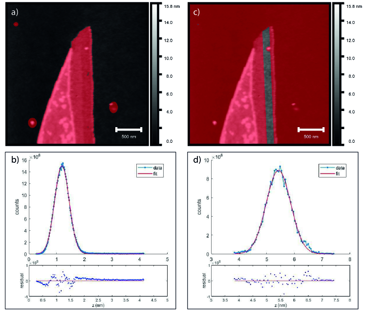
For all of the AFM data shown in this work, height measurements were found by averaging over large sample areas. This, as opposed to measuring individual line profiles, is a more robust way of determining the height, particularly if the sample surface is rough. First, the z-channel image is leveled until the width of a histogram of the entire substrate area is equal to the measurement noise. Then, Gaussean fits (of the form ) are found for each sample area. gives the mean z-channel value and gives the uncertainty of the z-channel value. The substrate mean was subtracted from each sample area mean to determine the sample area height (). Uncertainties were found by adding the Gaussean fit widths in quadrature as . Figure S2 shows an example of the masks and histograms used to evaluate the first layer height measured using ncAFM, where Figure S2a and b show the substrate mask, histogram, and fit, and c and d show the first layer mask, histogram, and fit. The AFM height results are shown in Figure 1(h-i), and a summary is presented in tabular form in Table 1.
| Location | Method | Height (nm) |
| Flake 1 | ||
| Substrate | Tapping Mode | 0.0 0.5 |
| NC-AFM | 0.0 1.6 | |
| KPFM | 0.0 0.5 | |
| 1st layer | Tapping Mode | 6.5 1.5 |
| NC-AFM | 6.0 1.9 | |
| KPFM | 3.9 0.6 | |
| Flake 2 | ||
| Substrate | Tapping Mode | 0.0 0.3 |
| NC-AFM | 0.0 0.4 | |
| KPFM | 0.0 0.2 | |
| 1st layer | Tapping Mode | 3.5 0.6 |
| NC-AFM | 4.2 0.5 | |
| KPFM | 3.1 0.5 | |
| 2nd layer | Tapping Mode | 4.1 0.6 |
| NC-AFM | 5.4 0.5 | |
| KPFM | 3.6 0.4 | |
| 3rd layer | Tapping Mode | 5.8 0.5 |
| NC-AFM | 7.9 0.9 | |
| KPFM | 8.4 0.4 | |
| 4th layer | Tapping Mode | 7.8 0.8 |
| NC-AFM | 10.9 1.1 | |
| KPFM | 9.0 0.4 | |
AFM surface roughness measurements
The surface roughness was measured using Gwyddion by masking the various regions of the sample (as in Figure S2) and measuring the root mean square (RMS) roughness. (Note that these roughness values very closely agree with the height uncertainties found by taking the histogram width of each layer, shown in Table 2.)
| Location | Method | RMS Roughness (nm) |
| Flake 1 | ||
| Substrate | Tapping Mode | 0.4 |
| NC-AFM | 1.1 | |
| KPFM | 0.4 | |
| 1st layer | Tapping Mode | 1.7 |
| NC-AFM | 1.1 | |
| KPFM | 0.7 | |
| Flake 2 | ||
| Substrate | Tapping Mode | 0.2 |
| NC-AFM | 0.3 | |
| KPFM | 0.2 | |
| 1st layer | Tapping Mode | 0.6 |
| NC-AFM | 0.5 | |
| KPFM | 0.4 | |
| 2nd layer | Tapping Mode | 0.6 |
| NC-AFM | 0.6 | |
| KPFM | 0.5 | |
| 3rd layer | Tapping Mode | 0.4 |
| NC-AFM | 0.6 | |
| KPFM | 0.3 | |
| 4th layer | Tapping Mode | 0.8 |
| NC-AFM | 1.2 | |
| KPFM | 0.4 | |
Flake 1 fold line trace
A line trace taken across the fold on Flake 1 is shown in Figure S3 below, with height measurements taken as the average of the z height along the single line. The uncertainty on the height value is given by the standard deviation of the z data along each line indicated in the graph. The small size and irregularity of the fold prevents a height measurement by the area averaging method, and the purpose of the line trace shown is to demonstrate a comparison of the step heights rather than accurate height values.
Photoluminescence measurements
The photoluminescence spectra in Figure 2 were analyzed and plotted in MATLAB. To remove random background noise artefacts in the data, the spectra were cleaned up using the function smooth(data,0.05,’rloess’), a local regression using weighted linear least squares and a 2nd degree polynomial model. Lower weight is assigned to outliers in the regression; the method assigns zero weight to data outside six mean absolute deviations. The data was smoothed using this method using a span of 5 of the total number of data points. The background signal from the SiO2 was subtracted from the MoSe2 curves. The peak position and associated uncertainty were obtained as follows: The main peaks were fitted to a Lorentzian function where is the height of the peak, is the position of the peak (wavelength), and is the width of the peak at half maximum [33]. The fitting was carried out in MATLAB (using fit function), with the appropriate starting parameters estimated. The error in the peak locations was found by forcibly varying around the fitted output value (while letting and vary), to find the range of for which the coefficient of determination (r-squared) value of the fit stayed within 0.01 of its optimum. R-squared indicates the proportionate amount of variation in the response variable y explained by the independent variables x in the linear regression model. The larger the r-squared is, the more variability is explained by the linear regression model. R-squared is the proportion of the total sum of squares explained by the model: where is the sum of squared regression, is the sum of squared total, and is the sum of squared error.