Using In-Plane Anisotropy to Engineer Janus Monolayers of Rhenium Dichalcogenides
Abstract
The new class of Janus two-dimensional (2D) transition metal dichalcogenides with two different interfaces is currently gaining increasing attention due to the possibility to access properties different from the typical 2D materials. Here, we show that in-plane anisotropy of a 2D atomic crystal, like ReS2 or ReSe2, allows formation of a large number of inequivalent Janus monolayers. We use first-principles calculations to investigate the structural stability of 29 distinct ReX2-xYx () structures, which can be obtained by selective exchange of exposed chalcogens in a ReX2 monolayer. We also examine the electronic properties and work function of the most stable Janus monolayers and show that the large number of inequivalent structures provides a way to engineer spin-orbit splitting of the electronic bands. We find that the breaking of inversion symmetry leads to sizable spin splittings and spontaneous dipole moments that are larger than those in other Janus dichalcogenides. Moreover, our calculations suggest that the work function of the Janus monolayers can be tuned by varying the content of the substituting chalcogen. Our work demonstrates that in-plane anisotropy provides additional flexibility in sub-layer engineering of 2D atomic crystals.
I Introduction
Symmetry is a powerful unifying principle in science and the study of symmetry breaking is one of the central questions in physics. In Janus materials, broken symmetry is made explicit by the formation of two interfaces with different chemical compositions and, hence possibly, dissimilar properties [1]. While such a concept was initially realised at the micrometer scale with spherical glass beads [2], more recently, atomically thin Janus materials became reality by engineering of two-dimensional (2D) atomic crystals like graphene and transition metal dichalcogenides (TMDs) [3, 4, 6, 5, 7, 8]. The latter are built of sandwich-like layers in which an atomic plane of transition metals is embedded between two planes of chalcogen atoms, and it has been shown that it is possible to produce Janus TMD layers in which these outer planes are made of different chalcogens. In their pioneering work, Lu et al. have successfully synthesized Janus MoSSe with a spontaneous out-of-plane dipole by selenization of MoS2 [3] while Zhang et al. have fabricated a monolayer Janus MoSeS by sulfurization of MoSe2 [4]. More recently, Sant et al. have also demonstrated a monolayer Janus PtSeS by sulfurization of PtSe2 [5]. Janus 2D materials present an interesting contrast to the idea of stacking 2D materials on top of each other into van der Waals heterostructures; [9] here instead, one engineers a single monolayer crystal. Janus TMDs in particular have several interesting properties including a strong Rashba spin splitting, second-harmonic response, piezoelectricity and good catalytic performance [6, 7, 8, 10].
In most TMDs, all of the chalcogen sites in the same plane are equivalent due to the combination of and translational symmetries present in the most common trigonal prismatic and octahedral phases [11]. We use the example of rhenium-based TMDs to show that 2D materials with lower symmetry provide an additional flexibility in the design of Janus materials, as inequivalence of atomic sites translates into potential chemical and physical site selectivity. In the case of ReS2 and ReSe2, the ideal octahedral (T) arrangement of chalcogens around the transition metal sites, Fig. 1(a), is distorted into characteristic rhenium chains [12, 13], as shown in Fig. 1(b). In the new structure (T′), breaking of the symmetry leaves inversion as the only non-trivial symmetry. We use density functional theory calculations to assess the energetic stability and electronic structure of ReS2-xSex and ReSe2-xSx monolayer crystals obtained by exchanging chalcogen species in inequivalent sites in one of the chalcogen planes. We show that in rhenium TMDs this allows the formation of a large number of different Janus monolayers. We identify the most stable structures, discuss their dynamical stability and investigate their work function and electronic properties, including the spin-orbit splitting and out-of-plane dipole moment arising due to broken inversion symmetry in the Janus layers. Notably, in ReSSe we find the dipole moment to be about four times larger than that reported for other Janus TMDs [14, 15].
Note that several different distortion-driven unit cells, some of which are only metastable, have been observed in TMDs [11, 16, 17]. All of the distorted unit cells share the two features relevant here: (i) the symmetry of the ideal T phase is broken while (ii) the inversion symmetry is preserved. Hence, our conclusions regarding the potential richness of Janus monolayers of ReX2-xYx can be generalised to these other distorted structures.

II Methods
Calculations are carried out using density functional theory (DFT) [18] as implemented in the Quantum Espresso simulation package [19, 20]. The Kohn-Sham wavefunctions and energies are calculated using the local density approximation (LDA) in the Perdew-Zunger parametrization [21], using a plane-wave basis with energy and charge density cutoffs of 60 and 360 Ry, respectively. Projector augmented-wave pseudopotentials [22] are used to describe the core-valence interactions. The structural relaxation is performed until the force on each atom is smaller than 0.005 eV/Å. The Brillouin Zone integration is sampled following the Monkhorst-Pack scheme [23], using 991 and 13131 -point grids for the ionic optimization and the electronic structure analysis, respectively. To avoid spurious interactions between periodically repeated slabs, the vacuum region is set to 25 Å, and dipole corrections were included to eliminate artificial electrostatic effects. When calculating the formation energies, we have checked that for an enlarged unit cell (for example, with the lattice constant doubled from to ), the conclusions regarding the energetic stability follow the same trend.
For more accurate band gaps, we have employed the HSE06 hybrid functional [24, 25], instead of the more computationally expensive GW methods [26, 27, 28], starting from the exchange-correlation energy expressed by LDA, including spin-orbit coupling.
The phonon band structures were calculated using density functional perturbation theory (DFPT) [29] in the Quantum Espresso code. The dynamic matrix was estimated on a -point mesh in the Brillouin zone; such sampling is found to be sufficient for obtaining well-converged results. The dynamical matrices at arbitrary wave vectors were obtained using Fourier Transform-based interpolation to obtain phonon dispersion along the same wave vector path as the electronic band structures.
The crystal orbital Hamilton populations (COHP) [30] presented in the Supplemental Material [31] were computed using the LOBSTER code [32, 33]. We employed the local basis function as given by Bunge [34] for the projection of the 3 and 3 orbitals for S, 4 and 4 for Se, and 5, 6, 5, and 5 for Re atoms. For the charge density analysis, we performed integrations of the electronic charge of the atoms following Bader charge method implemented in Henkelman’s code [35, 36, 37, 38].
III Results and Discussion
III.1 Energetic stability and structural properties
We start our discussion with a closer look at a unit cell of monolayer ReX2, , as shown in the inset of Fig. 1(b). Due to a Jahn-Teller distortion, the lattice vectors of the distorted T′ structure are approximately twice as large as in the ideal T phase and the unit cell contains 12, rather than 3, atoms – 4 rheniums and 8 chalcogens [12, 13]. As inversion is the only point group symmetry element still present, all four of the chalcogen sites on the same side of the transition metals (either above or below) are inequivalent. We highlight one set of such sites in the inset of Fig. 1(b) and number them as 1, 2, 3, and 4. The low symmetry of the unit cell of monolayer rhenium dichalcogenides results in a Brillouin zone which is a distorted regular hexagon, as shown in Fig. 1(c), where we have labeled the inequivalent corners and centres of sides and marked a path in the momentum space used to plot the band structures later on.
In the bulk, the inequivalence of chalcogen sites has been observed explicitly by studying the Raman spectra of ReSe2-xSx alloys containing low levels of sulfur [39] and investigating ReSe2 using tunnelling microscopy [40]. In the former study, four different Raman bands arising from the local vibrational modes of sulfur atoms were observed, corresponding to substitutions occupying each of the sites. Interestingly, because in ReX2 the valence band maximum is predominantly built from in-plane rhenium -orbitals [13, 41], a unique coupling develops between the crystal thickness and in-plane anisotropy of the electronic dispersion: the anisotropy increases as the crystal is thinned down and reaches maximum in the monolayer [42]. This suggests that rhenium TMD monolayers are an ideal platform to explore how in-plane anisotropy of 2D crystals can be used to engineer novel atomically thin Janus materials.
Recently, Janus TMD monolayers have been produced by exchange of chalcogens in the layer above the transition metals either by sulfurization of a selenide [4] or selenization of a sulfide [3]. In particular, Zhang et al. demonstrated a fine degree of control over the sulphurization of MoSe2 as a function of the temperature of the process [4]. An even greater degree of control was achieved by Lin et al. who used pulsed laser deposition [43] and tuned kinetic energy of Se plasma to determine conditions for the formation of high-quality Janus WSSe monolayers at temperatures below 300 ∘C.
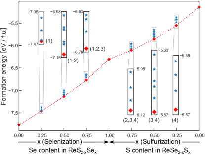
In hexagonal TMDs, such processes cannot distinguish between various chalcogen sites as they are related by the rotational symmetry and lattice translation. However, as in ReX2 the chalcogen sites 1-4 are inequivalent, it could be possible to devise a process which will exchange the chalcogens selectively rather than en masse. In the rest of the paper, we use the notation ReX2-xYx(), with concentration , to denote a monolayer of ReX2 in which 4 of the X atoms in positions as marked in the inset of Fig. 1(b) have been substituted with Y chalcogens. In this notation, is the fraction of all chalcogen sites that have been exchanged and, for example, ReSe1.5S0.5(1,3) denotes a ReSe2 monolayer in which selenium atoms in positions 1 and 3 have been replaced by sulphur. For Janus layers in which all of the top four chalcogens have been substituted, the indices and substitution positions can be omitted without loss of clarity. Moreover, since in our calculations we model free-standing monolayers, the two “full Janus” structures, ReSeS and ReSSe, are structurally and electronically equivalent. In total, we obtain 29 distinct Janus structures and we present the formation energies for all of them as well as those of pristine ReS2 and ReSe2 monolayers in Fig. 2 (in the Supplemental Material [31], we also present the data from Fig. 2 in the form of the binary convex hull, Fig. S1, in which the formation energies of the Janus monolayers are directly compared to those of the pristine ReS2 and ReSe2 monolayers).
To evaluate the energetic stability of our structures, we have calculated the formation energies per formula unit (f. u.),
| (1) | ||||
where is the total energy of each compound and are the chalcogen species. For the pure elements S and Se, we have taken as reference formation energies of their most stable crystalline phases at ambient conditions (monoclinic for Se and orthorhombic for S). The results in Fig. 2 show that the pristine ReS2 and ReSe2 monolayers have, respectively, the lowest (-7.77 eV per f. u.) and the highest (-5.15 eV per f. u.) formation energies among all the investigated structures. The formation energies of all the Janus layers fit between these two values, with energetic stability decreasing (and the value of increasing) linearly with the increasing of the selenium content. This suggests that it is energetically more convient to engineer the Janus monolayers by sulfurization of ReSe2 rather than selenization of ReS2.
The formation energy of a full Janus layer ReSSe is -6.30 eV, which is close to the mean value (-6.46 eV) of the formation energies of the pristine monolayers. We have checked that, for ReSSe, our calculations predict the same formation energy, irrespectively of whether we consider a selenized ReS2 or a sulphurized ReSe2. All other structures with the same chalcogen concentrations have different formation energies because, as suggested by the in-plane anisotropy of rhenium dichalcogenides, exchange of chalcogens on each of the four inequivalent sites corresponds to dissimilar energy costs. The formation energies of the ReS1.75Se0.25() structures, in the left half of Fig. 2, show that ReS1.75Se0.25(1) is the most stable ( eV per unit cell), followed by ReS1.75Se0.25(2), ReS1.75Se0.25(3) and ReS1.75Se0.25(4) with formation energies higher by 4 meV, 40 meV, and 86 meV, respectively. Similar site ordering, , is seen for a step-by-step selenization of ReS2 into ReSSe as ReS1.75Se0.25(1), ReS1.5Se0.5(1,2) and ReS1.25Se0.75(1,2,3) are the most stable structures for , and , respectively. To note, the very small energy difference between ReS1.75Se0.25(1) and ReS1.75Se0.25(2) means that both configurations are likely to form for the of selenide concentration. Notably, as seen from the location of sites 1 and 2 in Fig. 1(b), exchange of sulfur to selenide is preferential at the chalcogen sites between the rhenium chains. This is in agreement with the observations of preferential Se locations in ReS2-xSex alloy [44]. Overall, we find that for a Se atom substituting sulfur, the distances to its three nearest rhenium atoms increase by as much as 5.5%.
The energy ordering of the chalcogen sites preferred during sulfurization of a ReSe2 monolayer, right half of Fig. 2, is reversed with respect to that discussed for ReS2-xSex: the most stable configurations are ReSe1.75S0.25(4), ReSe1.5S0.5(3,4), and ReSe1.25S0.75(2,3,4) for , and , respectively. Similarly, for the ReSe1.75S0.25 structure, the energetic stability of the sites follows the sequence 4, 3, 2, and 1 from the most to the least stable – inversed as compared to that of the ReS1.75Se0.25 monolayer. Together with the earlier results for selenization of ReS2, this means that the energetics of chalcogen substitution at any of the inequivalent sites can be considered effectively independent of what chalcogen species occupy the other sites. Moreover, such energetic ordering of the sites implies that sulfur prefers to substitute selenide at atomic positions located within the rhenium chains rather than between them. This can be explained by the difference in the size of the chalcogen species and the distorted structure of the T′ phase. Due to the distortion, as compared to the T phase, the bond lengths between rhenium atoms and the chalcogen atoms between the chains (sites 1 and 2) are stretched while the bond lengths between rheniums and the chalcogens within the chain (sites 3 and 4) are shortened. Therefore, it is energetically easier to accommodate bigger chalcogen species (Se) between the chains as there is more space available as compared to within the chains. At the same time, the smaller chalcogen species (S) can fit within the rhenium chains with less effort against the local strain. We find that when one sulfur replaces a selenide atom, the bond length is shortened by 5.3% on site 1, compared to a value of 4.8% on the other sites. To note, the energetic order of chalcogen vacancies in ReX2 follows the sequence 4, 3, 2, 1 [45, 46], the same as for exchange of Se to S. In both cases, the order is dictated by the preference for atomic sites corresponding to smaller volume in the lattice to minimize strain (either due to an empty site or substitution by an atom smaller than Se). The same mechanism reverses the site ordering for selenization of ReS2 to accommodate larger Se atoms in place of smaller S.
We have investigated whether exchange of the chalcogen species leads to significant changes in the bond strength by computing the Crystal Orbital Hamilton Populations (COHP) [30] for the three shortest chalcogen-rhenium bonds for each of the chalcogen sites for ReS2 and ReS1.75Se0.25(1). COHP partitions the band structure energy into orbital-pair interactions and can be interpreted as a ”bond-weighted” density-of-states between a pair of atoms. It indicates the bonding character of states at given energy and its energy integral shows the contribution of a specific bond to the band energy and hence provides information about the bond strength. Our results presented in Fig. S2 in the Supplemental Material [31] show little change in the COHP upon the exchange of one S to Se, indicating very similar bonds in both monolayers despite their significant lengthening in ReS1.75Se0.25(1) as compared to ReS2. This suggests that interpretation of our results in terms of strain and chalcogen sites which can more readily accommodate the larger/smaller chalcogen species does capture the essential physics.
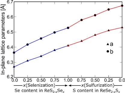
The impact of the size of the chalcogen species on the structure of the Janus monolayer can also be seen by comparing their in-plane lattice constants, and , shown in Fig. 3 for the pure monolayers and the most stable Janus crystals. Both vary nearly linearly between ReS2 and ReSe2 with chalcogen composition conforming to Vegard’s law, which postulates the existence of a linear relationship between the crystal lattice constant of an alloy and the varying concentration of its constituents [47]. The lattice constants , of a Janus monolayer ReX2-xYx can be determined as
| (2) |
where , , Å, Å, Å and Å. For example, for the full Janus monolayer ReSSe, Å, in agreement with our ab initio calculations.
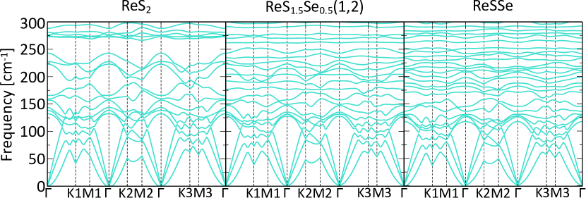
Finally, apart from thermodynamic stability of the studied Janus monolayers, we also investigate their dynamic stability by studying their phonon spectra. In Fig. 4, we show the phonon band structures for three selected materials: pristine ReS2, ReS1.5Se0.5(1,2) and ReSSe, calculated along the wave vector path as shown in Fig. 1(c). We do not observe any appearance of imaginary energy solutions, indicating no instabilities or softening of the phonon modes. We suggest that this is because the low symmetry of the pristine ReX2 compounds easily accommodates small distortions of bonds due to SSe substitutions. Spectra for all the structures are very similar in the range of small wavenumbers, cm-1. At higher wavenumbers, exchanging S to Se in ReS2 lowers the energy of optical phonons which leads to vanishing of the gap present in ReS2 around cm-1 and flattening of their dispersion. This is due to the heavier mass of Se as compared to S [39].
III.2 Electronic properties
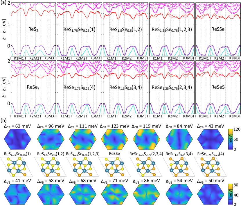
Following our discussion of the stability of the various ReX2-xYx Janus monolayers, we discuss the electronic properties of only the most stable structures for each concentration. Figure 5(a) presents the band structures of these ReX2-xYx systems, from the pristine ReS2 and ReSe2 monolayers on the left (top and bottom row, respectively) to the full Janus structures, ReSSe and ReSeS, on the right. The momentum path through the Brillouin zone is chosen as indicated with the red arrows in Fig. 1(c). As anticipated, the bands of ReSSe and ReSeS (right-most column) are identical. Due to the intrinsically present inversion symmetry, the bands of both the pristine ReS2 and ReSe2 monolayers (left-most column) are spin-degenerate. Also, within our computational framework, both are indirect band gap semiconductors: the conduction band minimum (CBM) is found at whereas the valence band maximum (VBM) is located slightly away from it. This is in agreement with other works using similar methodology [42, 48] although a direct band gap has been predicted at the GW level [49] (interestingly, the latter also predicts direct band gaps in the bulk while experiments suggest this is not the case [50, 51, 52, 53]). All of the Janus monolayers inherit the CBM location as well as the shape of the valence band around from the pristine structures and remain indirect band gap semiconductors. However, exchange of any chalcogens only on one side of the transition metals breaks the inversion symmetry so that spectra of all Janus monolayers display band splitting due to spin-orbit coupling. While in general this splitting increases as the concentration of the substituting chalcogen (and hence the extent of inversion symmetry breaking) increases, for a given momentum it does not simply grow linearly in magnitude from either of the pristine structures to the full Janus monolayer. In Fig. 5(b), we show the momentum-resolved 2D maps of the spin-splitting of the non-degenerate lowest conduction and highest valence bands across the whole Brillouin zone and list the maximum conduction and valence band splittings, and , respectively, for all the Janus structures. Notice that, in the valence band in particular, the regions of the Brillouin zone with the largest splitting change from one structure to the next and are not always found in the vicinity of high-symmetry directions in the Brillouin zone. Moreover, the largest possible valence band splitting is produced in ReSe1.25S rather than in the full Janus monolayer ReSSe. This suggests sub-layer atomic engineering of two-dimensional crystals as a potential strategy of tailoring the momentum-dependence of spin-orbit coupling.
While the band structures presented in Fig. 5 have been obtained in the LDA approximation, this method is well-known to provide underestimated band gaps. We performed additional calculations with HSE-type hybrid functional to produce more reliable band gap estimates. We list the LDA and HSE values for the most stable ReS2-xSex and ReSe2-xSx monolayers in the first two columns of Table 1. Overall, the LDA band gaps are enlarged by about 50% when HSE is used. Upon substitution of ReS2 (ReS2) with Se (S), the band gap decreases (increases), reaching the value of 1.86 eV for the full Janus monolayer. However, unlike the lattice constant, which follows Vegard’s law, the the band gap does not show a linear change with concentration since the band gaps of ReS1.25Se0.75 and ReSe1.25S0.75 are sightly larger than or equal to those of ReS1.5Se0.5 and ReSe1.5S0.5, respectively (See Table 1).
| Structure | LDA gap | HSE gap | |
|---|---|---|---|
| ReS2 | 1.39 | 2.06 | 0.00 |
| ReS1.75Se0.25(1) | 1.28 | 1.92 | 0.14 |
| ReS1.5Se0.5(1,2) | 1.24 | 1.88 | 0.30 |
| ReS1.25Se0.75(1,2,3) | 1.26 | 1.89 | 0.50 |
| ReSSe / ReSeS | 1.24 | 1.86 | 0.71 |
| ReSe1.25S0.75(2,3,4) | 1.16 | 1.76 | 0.56 |
| ReSe1.5S0.5(3,4) | 1.16 | 1.76 | 0.39 |
| ReSe1.75S0.25(4) | 1.19 | 1.79 | 0.21 |
| ReSe2 | 1.18 | 1.78 | 0.00 |
For the pristine ReS2 and ReSe2, our LDA gap values are in a good agreement with the previously reported DFT calculations [42, 48]. The more accurate values for the band gaps of the pristine single layers have been also calculated using the GW method, yielding 2.38 eV [48, 49] and 2.09 eV [48] or 2.05 eV [49] for ReS2 and ReSe2, respectively. Our HSE calculations underestimate these GW values by approximately 13%.
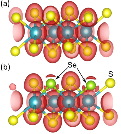
Another consequence of inversion-symmetry breaking is the formation of an out-of-plane dipole moment, , which arises due to the difference in electronegativities between the S and Se species [3, 54, 15, 14] and points towards the chalcogen layer with a greater concentration of selenium. The magnitude of increases with increasing concentration of the substituting chalcogen, , reaching maximum, Å, where is the magnitude of electron charge, in the full Janus monolayer. We list the dipole moment for the most stable structures (as well as, for explicit comparison, for the pristine structures which have no dipole moment) in Table 1. We compare the electron density distribution in the pristine ReS2 () and ReS1.5Se0.5(1,2) ( D) in Fig. 6. Incorporating Se in place of S leads to a decrease of the electron density around the respective Se atomic sites and a transfer of charge, mainly to the rhenium atoms. The electron density around the S sites in the same chalcogen layer as the Se atoms is effectively unchanged. As shown by Bader charge analysis [55, 35] presented in Table S1 of the Supplemental Material [31], the charge redistribution due to SSe exchange at a given site is only weakly affected by the changes in the atomic species occupying chalcogen sites in the vicinity. We find that the dipole moment values of Janus ReSSe/ReSeS are about four times as large as the values of their MoSSe and WSSe analogues [15, 14].
III.3 Work function
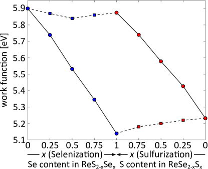
The exchange of chalcogen atoms also modifies the work function of the material. In Fig. 7, we show using the blue and red circles the work function, , taken here as the difference between the vacuum level and the valence band maximum, for all of the stable ReX2-xYx monolayers. We observe two nearly linear curves which show the work function for selenized ReS2 (blue circles) and sulfurized ReSe2 (red circles), respectively. For the former, the work function decreases linearly with the increasing concentration of Se, from 5.90 eV for ReS2 to 5.14 eV for the full Janus monolayer ReSSe, close to the work function of the pristine ReSe2 (5.24 eV). Inversely, the work function of sulfurized ReSe2 increases linearly to the value of 5.87 eV for the full Janus monolayer ReSeS. The discontinuity in in the centre of the graph is a consequence of the out-of-plane dipole moment . Recall that we assume here that exchange of the chalcogens takes place only in the layer above the transition metals which corresponds to the experimental situation of a monolayer crystal resting on a substrate with its top side exposed. As a result, the full Janus monolayer ReSSe obtained from ReS2 and ReSeS obtained from ReSe2 have dipole moments oriented in opposite directions with respect to the surface which leads to the difference in work functions (our rigid choice of ”up” and ”down” breaks the inversion symmetry which otherwise links the two structures). Therefore, as pointed out before [14], Janus TMDs provide interesting opportunities when considering band alignment in vertical or planar heterojunctions. For completeness, we also show in Fig. 7 the work functions computed for the bottom surfaces of all structures, shown using blue and red squares (and a black dashed line as a guide for the eye) for selenized ReS2 and sulfurized ReSe2, respectively. For a given structure, the difference between the work functions indicated with a square and a circle corresponds to the difference of electric potential energies of the two chalcogen layers.
IV Conclusions
In summary, we have employed first-principles density functional simulations to study the stability as well as lattice and electronic properties of Janus monolayers of rhenium dichalcogenides. We have shown that the in-plane anisotropy of rhenium dichalcogenides leads to energetical inequivalence of Janus-like monolayers with the same sulfur and selenium content. While the selenium atoms prefer occupation of the interchain chalcogen sites, sulfur favours intrachain sites instead. In general, 2D alloys are thermodynamically preferred over their 2D Janus counterparts where S and Se atoms are separated from each other on either side of the (top or bottom) surfaces. However, recent experimental work demonstrates significant improvement of the understanding and degree of control of the chalcogen exchange process, aimed at preventing alloying and realizing Janus geometry [3, 4, 5, 43, 56, 57]. This, coupled with the anisotropy-induced inequivalence of the chalcogen sites means that, at least in principle, in ReX2 it could be possible to selectively exchange only a fraction of the chalcogens in a layer in contrast to all of them as is the case for other Janus TMDs. Such a partial chalcogen substitution provides a way to tune the work function of the material. Moreover, it enables a gradual breaking of inversion symmetry and hence engineering of spin-orbit splitting of the electronic bands in a 2D material. Finally, inversion symmetry breaking induces out-of-plane dipoles which in the full Janus monolayer are significantly larger than those reported for other Janus TMDs. Overall, our findings highlight the unusual properties of Janus rhenium dichalcogenides and, more generally, the relevance of in-plane anisotropy when engineering 2D materials.
Acknowledgements.
This work was supported by the U.K. Engineering and Physical Sciences Research Council (EPSRC) through the Centre for Doctoral Training in Condensed Matter Physics, Grant EP/L015544/1. We acknowledge use of the Balena High Performance Computing (HPC) Service at the University of Bath as well as the Isambard UK National Tier-2 HPC Service operated by GW4 and the UK Met Office and funded by EPSRC (Grant EP/P020224/1). For the purpose of open access, the authors have applied a Creative Commons Attribution (CC BY) licence to any Author Accepted Manuscript version arising. The data used in this study can be reproduced using the files available from the University of Bath data archive at https://doi.org/10.15125/BATH-001136 [58].References
- [1] A. Walther and A. H. E. Muller, Janus Particles: Synthesis, Self-Assembly, Physical Properties, and Applications, Chemical Reviews 113, 5194 (2013).
- [2] C. Casagrande, P. Fabre, E. Raphael, and M. Veyssie, Janus Beads: Realization and Behaviour at Water/Oil Interfaces, Europhysics Letters 9, 251 (1989).
- [3] A.-Y. Lu, H. Zhu, J. Xiao, C.-P. Chuu, Y. Han, M.-H. Chiu, C.-C. Cheng, C.-W. Yang, K.-H. Wei, Y. Yang, Y. Wang, D. Sokaras, D. Nordlund, P. Yang, D. A. Muller, M.-Y. Chou, X. Zhang, and L.-J. L. Lu, Janus monolayers of transition metaldichalcogenides, Nature Nanotechnology 12, 744 (2017).
- [4] J. Zhang, S. Jia, I. Kholmanov, L. Dong, D. Er, W. Chen, H. Guo, Z. Jin, V. B. Shenoy, L. Shi, and J. Lou, Janus Monolayer Transition-Metal Dichalcogenides, ACS Nano 11, 8192 (2017).
- [5] R. Sant, M. Gay, A. Marty, S. Lisi, R. Harrabi, C. Vergnaud, M. T. Dau, X. Weng, J. Coraux, N. Gauthier, O. Renault, G. Renaud, and M. Jamet, Synthesis of epitaxial monolayer Janus SPtSe, npj 2D Materials & Applications 4, 41 (2020).
- [6] R. Li, Y. Cheng, and W. Huang, Recent Progress of Janus 2D Transition Metal Chalcogenides: From Theory to Experiments, Small 14, 1802091 (2018).
- [7] M. Yagmurcukardes, Y. Qin, S. Ozen, M. Sayyad, F. M. Peeters, S. Tongay, and H. Sahin, Quantum properties and applications of 2D Janus crystals and their superlattices, Applied Physics Reviews 7, 011311 (2020).
- [8] L. Zhang, Z. Yang, T. Gong, R. Pan, H. Wang, Z. Guo, H. Zhang, and X. Fu, Recent advances in emerging Janus two-dimensional materials: from fundamental physics to device applications, Journal of Materials Chemistry A 8, 8813 (2020).
- [9] A. K. Geim and I. V. Grigorieva, Van der Waals heterostructures, Nature 499, 419 (2013).
- [10] X. Yuan, M. Yang, L. Wang, and Y. Li, Structural stability and intriguing electronic properties of two-dimensional transition metal dichalcogenide alloys, Physical Chemistry Chemical Physics 19, 13846 (2017).
- [11] S. Manzeli, D. Ovchinnikov, D. Pasquier, O. V. Yazyev, and A. Kis, 2D transition metal dichalcogenides, Nature Reviews Materials 2, 17033 (2017).
- [12] H.-J. Lamfers, A. Meetsma, G. Wiegers, and J. de Boer, The crystal structure of some rhenium and technetium dichalcogenides, Journal of Alloys and Compounds 241, 34 (1996).
- [13] M. Kertesz and R. Hoffmann, Octahedral vs trigonal-prismatic coordination and clustering in transition-metal dichalcogenides, Journal of the American Chemical Society 106, 3453 (1984).
- [14] A. C. Riis-Jensen, M. Pandey, and K. S. Thygesen, Efficient Charge Separation in 2D Janus van der Waals Structures with Built-in Electric Fields and Intrinsic p–n Doping, Journal of Physical Chemistry C 122, 24520 (2018).
- [15] C. Xia, W. Xiong, J. Du, T. Wang, Y. Peng, and J. Li, Universality of electronic characteristics and photocatalyst applications in the two-dimensional Janus transition metal dichalcogenides, Physical Review B 98, 165424 (2018).
- [16] X. Qian, J. Liu, L. Fu, J. Li, Quantum spin Hall effect in two-dimensional transitionmetal dichalcogenides, Science 346, 1344 (2014).
- [17] M. S. Sokolikova and C. Mattevi, Direct synthesis of metastable phases of 2D transition metal dichalcogenides, Chemical Society Reviews 49, 3952 (2020).
- [18] W. Kohn and L. J. Sham, Self-Consistent Equations Including Exchange and Correlation Effects, Physical Review 140, A1133 (1965).
- [19] P. Giannozzi, S. Baroni, N. Bonini, M. Calandra, R. Car, C. Cavazzoni, D. Ceresoli, G. L. Chiarotti, M. Cococcioni, I. Dabo, A. Dal Corso, S. de Gironcoli, S. Fabris, G. Fratesi, R. Gebauer, U. Gerstmann, C. Gougoussis, A. Kokalj, M. Lazzeri, L. Martin-Samos, N. Marzari, F. Mauri, R. Mazzarello, S. Paolini, A. Pasquarello, L. Paulatto, C. Sbraccia, S. Scandolo, G. Sclauzero, A. P. Seitsonen, A. Smogunov, P. Umari, and R. M. Wentzcovitch, QUANTUM ESPRESSO: a modular and open-source software project for quantum simulations of materials, Journal of Physics: Condensed Matter 21, 395502 (2009).
- [20] P. Giannozzi, O. Andreussi, T. Brumme, O. Bunau, M. Buongiorno Nardelli, M. Calandra, R. Car, C. Cavazzoni, D. Ceresoli, M. Cococcioni, N. Colonna, I. Carnimeo, A. Dal Corso, S. de Gironcoli, P. Delugas, R. A. DiStasio Jr, A. Ferretti, A. Floris, G. Fratesi, G. Fugallo, R. Gebauer, U. Gerstmann, F. Giustino, T. Gorni, J. Jia, M. Kawamura, H.-Y. Ko, A. Kokalj, E. Kucukbenli, M. Lazzeri, M. Marsili, N. Marzari, F. Mauri, N. L. Nguyen, H.-V. Nguyen, A. Otero-de-la-Roza, L. Paulatto, S. Ponce, D. Rocca, R. Sabatini, B. Santra, M. Schlipf, A. P. Seitsonen, A. Smogunov, I. Timrov, T. Thonhauser, P. Umari, N. Vast, X. Wu, and S. Baroni, Advanced capabilities for materials modelling with Quantum ESPRESSO, Journal of Physics: Condensed Matter 29, 465901 (2017).
- [21] J. P. Perdew and A. Zunger, Self-interaction correction to density-functional approximations for many-electron systems, Physical Review B 23, 5048 (1981).
- [22] P. E. Blöchl, Projector augmented-wave method, Physical Review B 50, 17953 (1994).
- [23] H. J. Monkhorst and J. D. Pack, Special points for Brillouin-zone integrations, Physical Review B 13, 5188 (1976).
- [24] J. Heyd, G. E. Scuseria, and M. Ernzerhof, Hybrid functionals based on a screened Coulomb potential, Journal of Chemical Physics 118, 8207 (2003).
- [25] J. Heyd, G. E. Scuseria, and M. Ernzerhof, Erratum: “Hybrid functionals based on a screened Coulomb potential” [J. Chem. Phys. 118, 8207 (2003)], Journal of Chemical Physics 124, 219906 (2006).
- [26] L. Hedin, New Method for Calculating the One-Particle Green’s Function with Application to the Electron-Gas Problem, Physical Review 139, A796 (1965).
- [27] M. S. Hybertsen and S. G. Louie, Electron correlation in semiconductors and insulators: Band gaps and quasiparticle energies, Physical Review B 34, 5390 (1986).
- [28] M. Schlipf, H. Lambert, N. Zibouche, and F. Giustino, SternheimerGW: A program for calculating GW quasiparticle band structures and spectral functions without unoccupied states, Computer Physics Communications 247, 106856 (2020).
- [29] S. Baroni, S. de Gironcoli, A. Dal Corso, and P. Giannozzi, Phonons and related crystal properties from density-functional perturbation theory, Reviews of Modern Physics 73, 515 (2001).
- [30] R. Dronskowski and P. E. Bloechl, Crystal orbital Hamilton populations (COHP): energy-resolved visualization of chemical bonding in solids based on density-functional calculations, Journal of Physical Chemistry 97, 8617 (1993).
- [31] See Supplemental Material at [URL will be inserted by publisher] for the discussion of the binary convex hull, crystal orbital Hamilton populations and Bader charge analysis.
- [32] S. Maintz, V. L. Deringer, A. L. Tchougreeff, and R. Dronskowski, Analytic Projection from Plane-Wave and PAW Wavefunctions and Application to Chemical-Bonding Analysis in Solids, Journal of Computational Chemistry 34, 2557 (2013).
- [33] S. Maintz, V. L. Deringer, A. L. Tchougreeff, and R. Dronskowski, LOBSTER: A Tool to Extract Chemical Bonding from Plane-Wave Based DFT, Journal of Computational Chemistry 37, 1030 (2016).
- [34] C. F. Bunge, J. A. Barrientos, and A. V. Bunge, Roothaan-Hartree-Fock Ground-State Atomic Wave Functions: Slater-Type Orbital Expansions and Expectation Values for Z=2-54, Atomic Data and Nuclear Data Tables 53, 113 (1993).
- [35] G. Henkelman, A. Arnaldsson, and H. Jonsson, A fast and robust algorithm for Bader decomposition of charge density, Computational Materials Science 36, 354 (2006).
- [36] E. Sanville, S. D. Kenny, R. Smith, and G. Henkelman, An improved grid-based algorithm for Bader charge allocation, Journal of Computational Chemistry 28, 899 (2007).
- [37] W. Tang, E. Sanville, and G. Henkelman, A grid-based Bader analysis algorithm without lattice bias, Journal of Physics: Condensed Matter 21, 084204 (2009).
- [38] M. Yu and D. R. Trinkle, Accurate and efficient algorithm for Bader charge integration, Journal of Chemical Physics 134, 064111 (2011).
- [39] L. S. Hart, J. L. Webb, S. Murkin, D. Wolverson, and D.-Y. Lin, Identifying light impurities in transition metal dichalcogenides: the local vibrational modes of S and O in ReSe2 and MoSe2, npj 2D Materials and Applications 1, 41 (2017).
- [40] M. Hong, X. Zhou, N. Gao, S. Jiang, C. Xie, L. Zhao, Y. Gao, Z. Zhang, P. Yang, Y. Shi, Q. Zhang, Z. Liu, J. Zhao, and Y. Zhang, Identifying the Non-Identical Outermost Selenium Atoms and Invariable Band Gaps across the Grain Boundary of Anisotropic Rhenium Diselenide, ACS Nano 12, 10095 (2018).
- [41] B. K. Choi, S. Ulstrup, S. M. Gunasekera, J. Kim, S. Y. Lim, L. Moreschini, J. S. Oh, S.-H. Chun, C. Jozwiak, A. Bostwick, E. Rotenberg, H. Cheong, I.-W. Lyo, M. Mucha-Kruczynski, and Y. J. Chang, Visualizing orbital content of electronic bands in anisotropic 2D semiconducting ReSe2, ACS Nano 14, 7880 (2020).
- [42] L. S. Hart, S. M. Gunasekera, M. Mucha-Kruczynski, J. L. Webb, J. Avila, M. C. Asensio, and D. Wolverson, Interplay of crystal thickness and in-plane anisotropy and evolution of quasi-one dimensional electronic character in ReSe2, Physical Review B 104, 035421 (2021).
- [43] Y.-C. Lin, C. Liu, Y. Yu, E. Zarkadoula, M. Yoon, A. A. Puretzky, L. Liang, X. Kong, Y. Gu, A. Strasser, H. M. Meyer III, M. Lorenz, M. F. Chisholm, I. N. Ivanov, C. M. Rouleau, G. Duscher, K. Xiao, and D. B. Geohegan, Low Energy Implantation into Transition-Metal Dichalcogenide Monolayers to Form Janus Structures, ACS Nano 14, 3896 (2020).
- [44] W. Wen, J. Lin, K. Suenaga, Y. Guo, Y. Zhu, H.-P. Hsud, and L. Xie, Preferential S/Se occupation in an anisotropic ReS2-xSe2x monolayer alloy, Nanoscale 9, 18275 (2017).
- [45] S. Horzum, D. Cakir, J. Suh, S. Tongay, Y.-S. Huang, C.-H. Ho, J. Wu, H. Sahin, and F. M. Peeters, Formation and stability of point defects in monolayer rhenium disulfide, Physical Review B 89, 155433 (2014).
- [46] Y. Zhu, L. Tao, X. Chen, Y. Ma, S. Ning, J. Zhou, X. Zhao, M. Bosman, Z. Liu, S. Du, S. T. Pantelides, and W. Zhou, Anisotropic point defects in rhenium diselenide monolayers, iScience 24, 103456 (2021).
- [47] L. Vegard, Die Konstitution der Mischkristalle und die Raumf ullung der Atome, Zeitschrift fur Physik 5, 17 (1921).
- [48] H.-X. Zhong, S. Gao, J.-J. Shi, and L. Yang, Quasiparticle band gaps, excitonic effects, and anisotropic optical properties of the monolayer distorted 1T diamond-chain structures ReS2 and ReSe2, Physical Review B 92, 115438 (2015).
- [49] J. Echeverry, and I. Gerber, Theoretical investigations of the anisotropic optical properties of distorted 1T-ReS2 and ReSe2 monolayers, bilayers, and in the bulk limit, Physical Review B 97, 075123 (2018).
- [50] J. L. Webb, L. S. Hart, D. Wolverson, C. Chen, J. Avila, and M. C. Asensio, Electronic band structure of ReS2 by high-resolution angle-resolved photoemission spectroscopy, Physical Review B 96, 115205 (2017).
- [51] L. S. Hart, J. L. Webb, S. Dale, S. J. Bending, M. Mucha-Kruczynski, D. Wolverson, C. Chen, J. Avila, and M. C. Asensio, Electronic bandstructure and van der Waals coupling of ReSe2 revealed by high-resolution angle-resolved photoemission spectroscopy, Scientific Reports 7, 5145 (2017).
- [52] P. Eickholt, J. Noky, E. F. Schwier, K. Shimada, K. Miyamoto, T. Okuda, C. Datzer, M. Druppel, P. Kruger, M. Rohlfing, and M. Donath, Location of the valence band maximum in the band structure of anisotropic 1T´-ReSe2, Physical Review B 97, 165130 (2018).
- [53] S. M. Gunasekera, D. Wolverson, L. S. Hart, and M. Mucha-Kruczynski, Electronic band structure of rhenium dichalcogenides, Journal of Electronic Materials 47, 4314 (2018).
- [54] Y. Ji, M. Yang, H. Lin, T. Hou, L. Wang, Y. Li, and S.-T. Lee, Janus Structures of Transition Metal Dichalcogenides as the Heterojunction Photocatalysts for Water Splitting, Journal of Physical Chemistry C 122, 3123 (2018).
- [55] R. F. W. Bader, Atoms in Molecules: A Quantum Theory, Oxford University Press, New York, 1990.
- [56] Y. Qin, M. Sayyad, A. R.-P. Montblanch, M. S. G. Feuer, D. Dey, M. Blei, R. Sailus, D. M. Kara, Y. Shen, S. Yang, A. S. Botana, M. Atature, and S. Tongay, Reaching the Excitonic Limit in 2D Janus Monolayers by In Situ Deterministic Growth, Advanced Materials 34, 2106222 (2022).
- [57] C. W. Jang, W. J. Lee, J. K. Kim, S. M. Park, S. Kim, and S.-H. Choi, Growth of two-dimensional Janus MoSSe by a single in situ process without initial or follow-up treatments, npg Asia Materials 14, 15 (2022).
- [58] N. Zibouche, S. M. Gunasekera, D. Wolverson, and M. Mucha-Kruczynski, Dataset for article Using In-Plane Anisotropy to Engineer Janus Monolayers of Rhenium Dichalcogenides, University of Bath Research Data Archive (2022), https://doi.org/10.15125/BATH-001136.