Origin of ferroelectric domain wall alignment with surface trenches in ultrathin films
Abstract
Engraving trenches on the surfaces of ultrathin ferroelectric (FE) films and superlattices promises control over the orientation and direction of FE domain walls (DWs). Through exploiting the phenomenon of DW-surface trench (ST) parallel alignment, systems where DWs are known for becoming electrical conductors could now become useful nanocircuits using only standard lithographical techniques. Despite this clear application, the microscopic mechanism responsible for the alignment phenomenon has remained elusive. Using ultrathin PbTiO3 films as a model system, we explore this mechanism with large scale density functional theory simulations on as many as 5,136 atoms. Although we expect multiple contributing factors, we show that parallel DW-ST alignment can be well explained by this configuration giving rise to an arrangement of electric dipole moments which best restore polar continuity to the film. These moments preserve the polar texture of the pristine film, thus minimizing ST-induced depolarizing fields. Given the generality of this mechanism, we suggest that STs could be used to engineer other exotic polar textures in a variety of FE nanostructures as supported by the appearance of ST-induced polar cycloidal modulations in this letter. Our simulations also support experimental observations of ST-induced negative strains which have been suggested to play a role in the alignment mechanism.
Ferroelectric (FE) domain walls (DWs) have been observed in parallel alignment with surface and substrate defects since the 2000’s [1, 2, 3, 4, 5]. While this phenomenon was initially proposed to control polarization dependent surface reactions [3], now that electrically conducting FE DWs [6, 7] have been realized, new horizons for nanoelectronic devices approach. That is, the phenomenon now promises control over the orientation of 2D conducting channels on the nanoscale; a potential pathway for fabricating DW-mediated nanocircuits with standard lithographical techniques. Presently, control over FE DWs and polar textures is achieved using carefully directed electric fields. With this technique, exotic topological phases including polar skyrmions [8] have been stabilized and DW-based nanocomponents [9, 10, 11, 12] have been created; the latter defining the emerging field of DW nanoelectronics via DW injection [13, 14, 15, 9, 16]. While directed electric fields offer the advantages of nanocircuits written with reversibility [7], they can lack permanence once the fields are released. Defect mediated alignment, however, offers enduring control without external stimuli. In light of this, we envisage great opportunities for these techniques to be applied in tandem helping to enable the next generation of DW-nanoelectronic devices.
Notwithstanding these advances, the mechanism for DW alignment with surface defects is far from a settled topic. One study used macroscopic time-dependent Landau–Ginzburg–Devonshire theory to examine the interaction of PbTiO3 (PTO)/SrTiO3 (STO) superlattices with the milled edges of the nanostructure [5]. They suggested that alignment arises from lowering the bulk and electrostrictive energy terms driven by the release of lateral mechanical restraints near the edge. Another study used a nanofocused X-ray beam to reveal giant strain and strain gradients near milled surface defects on the PTO/STO superlattice [4]. This opens the door to the possibility of piezoelectric and/or flexoelectric contributions to the alignment mechanism. Until the present letter, no microscopic origin for the phenomenon has been proposed.
The feature of the domain structure pinned in the alignment is also disputed. A density functional theory (DFT) study of steps on the PTO (001) surface [17] found that DWs formed exactly at the step edges, suggesting that the DWs themselves are pinned. In contrast, an effective Hamiltonian study [18] found that film stability was enhanced when the domain centroid (DC, the area of maximal out-of-plane polarization furthest from the DW) was pinned by the step edge. While the DFT study [17], in principle, should offer higher accuracy predictions, like-for-like comparisons cannot be made since the effective Hamiltonian study [18] treats the underlying flux-closure domain structure [19, 20] when the former does not. Indeed, providing a full treatment of FE domains with DFT quickly becomes intractable due to the (where is the number of atoms) scaling wall for computational time present in conventional DFT codes [21, 22].
In this letter, we address these discrepancies and offer a microscopic explanation of the DW alignment mechanism. Through performing state-of-the-art large scale DFT simulations of ultrathin PTO films, we venture far beyond previous works, able to treat the interaction between surface trenches (STs) and FE domains with DFT accuracy. We propose that DW-ST parallel alignment can be well explained by considering which ST orientations (relative to the DW) are best able to support continuity of the polar texture. This continuity minimizes new ST-induced depolarizing fields which would otherwise act to destabilize the polydomain polarization. We suggest that this alignment is only one consequence of a wider class of polar textures that can be produced through minimizing ST-induced depolarizing fields. This idea is reinforced by the appearance of engineered polar cycloidal modulations in our films.
To overcome the scaling wall of conventional DFT, the [22, 21] scaling algorithm [23, 24, 25] in the CONQUEST code [26, 27] (v1.0.5 [28]) is used with a single- plus polarization basis set of pseudoatomic orbitals [29, 30, 31], norm-conserving Hamann pseudopotentials [32, 33] and the local density approximation as parameterized by Perdew & Wang [34]. Other simulation details and preliminary tests are presented in the supplemental material [35].
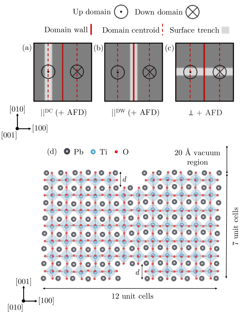
We begin with a polydomain and free-standing PbO terminated PTO film seven unit cells in thickness, with a 20 Å vacuum region in the out-of-plane direction to prevent interactions between film images. An epitaxial strain of - (relative to the the in-plane lattice parameters of bulk PTO) is imparted to represent the experimental PTO/STO lattice constant mismatch: the conditions where DW alignment has been experimentally observed [1, 2, 3, 4, 5]. Explicit STO substrate is not used as the incipient broken inversion symmetry in the out-of-plane directions is known to give rise to sizeable perturbations to the domain structure [36, 20] which we wish to isolate from our analysis. The equilibrium flux-closure domain period is used, which we find to be unit cells. One unit cell wide STs are placed on both surfaces of the film to (i) once again, limit the effect of inversion symmetry breaking and (ii) to eliminate spurious electric fields resultant from inequivalent surface dipole densities (otherwise requiring approximate correction [37]). STs are laterally separated by 12 unit cells in one of three positions: over the DC running parallel to the DW (, Fig. 1(a)), over the DW running parallel to the DW (, Fig. 1(b)) or running perpendicular to the DW (Fig. (1(c)). This last orientation features antiferrodistortive (AFD) modes since the even in-plane periodicity, broken surface symmetry and PbO termination will always invoke the AFD surface reconstruction [38] (enhanced surface octahedral rotations). We label these films + AFD. For fair comparison, we double the in-plane periodicity of to additionally consider + AFD films. We are then able to evaluate the impact of AFD modes on the DW alignment mechanism.
Each film listed so far is treated with ST depths of and unit cells with PbO terminated trench floors (shown in Fig. 1(d)). To investigate the effects of lateral interactions between STs, we perform two further simulations of the , films with STs separated by (). This sufficiently limits the overlap of ST-induced surface strain fields. We relax each structure until the magnitude of the force on each atom falls below eV/Å.
The relative stability of each film is given in Table I. It is clear immediately that the most stable ST arrangement treated in this letter is + AFD, true for and supporting the results of an effective Hamiltonian study [18]. The hierarchy of stabilities is preserved independently of the treated . In decreasing order we have + AFD, + AFD, + AFD and then the films without AFD modes: and . This hierarchy demonstrates that parallel DW-ST alignment is favoured, in good agreement with experimental observations [1, 2, 3, 4, 5]. For STs parallel to the DW, we see that part of this hierarchy is preserved independently of AFD modes. While this strongly implies that AFD modes play little-to-no role in the DW alignment mechanism, we do see that AFD modes greatly lower the total energy and lead to strong antiphase tilts (of ) at the surface which locally suppress polar modes in agreement with a study using a similar method [20]. Remarkably, these modes persist at a similar magnitude at the trench floor despite the broken connectivity with the surface octahedral tilt network. The film is also more stable than by 0.359 eV/1760 atoms; part of the hierarchy is unaffected by larger lateral ST separations, consistent with DW alignment observed for isolated defects [4]. It is clear now that the DW alignment mechanism is robust to the conditions tested in this letter.
| E - E( + AFD) [eV/FU] | |||||
|---|---|---|---|---|---|
| + AFD | + AFD | + AFD | |||
| 0 | +0.219 | +1.706 | +3.852 | +4.106 | |
| 0 | +0.361 | +0.881 | +4.089 | +4.095 | |
| 0 | +0.141 | +1.951 | +4.639 | +4.878 | |
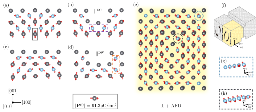
The stability of the different films can be best understood by considering how the polar texture adapts to a trench. That is, regardless of orientation, a trench must introduce new discontinuities to the polar texture of a pristine film (the film without STs) and therefore new depolarizing fields. The most stable arrangement must then be the one which best restores polar continuity, thus minimizing ST-induced depolarizing fields. Using this principle, the favorability of over can be understood clearly from the local polarization vector fields shown in Fig. 2(a-d). Independent of depth, we find that the local polarization near the DC for the film (Fig. 2(b)) is barely modulated in comparison to the DC of the pristine film (Fig. 2(a)). This is made clear by the two Ti-centered polarization vectors in the purple dashed box of Fig. 2(b) which reproduce the two surface modes present for the pristine film in the region for which the ST was inserted. This is because we have removed a unit cell at a site of preexisting out-of-plane polar discontinuity. The resulting polar texture arises from minimizing similar depolarizing fields to the pristine film. This contrasts greatly with the films (Fig. 2(d)) where there are large differences in the local polarization compared with the pristine film (Fig. 2(c)). In this case, the trench removes material in a region of continuous in-plane polarization at the cap of a polar vortex. This creates a new and large discontinuity in the polarization, giving rise to new in-plane depolarizing fields which are minimized by rotations of the local polarization at the trench edges towards [010] (or [00]) and [00]. While this minimization increases the stability of the film, the resulting polar texture sees the two Ti-centered local polar modes in the orange box of Fig. 2(d) stuck between a rock and a hard place. They are arranged in an electrostatically unfavorable near-head-to-head configuration. To compensate for this, the mean out-of-plane polarization of films are reduced by compared with films. All of these effects lower the stability of films.
The low stability of + AFD films can also be understood using the local polarization vector fields. This geometry is equivalent to interfacing an axial slice of the flux-closure domain structure of a thinner film with a thicker one. For example, at , a single unit cell wide and 3 unit cell thick axial slice is inserted (STs are present on both surfaces). This slice has weaker out-of-plane polarization than the surrounding 7 unit cell thick film; an experimentally observed effect for thinner pristine films [2]. In spite of this, the mean out-of-plane polarization for the entire film is greater than + AFD films. The same is not true for the axial polarization (along [010], the Bloch components [40]). These become highly discontinuous giving rise to new depolarizing fields which are compensated for by strongly reducing the axial polarization. Discontinuity perpendicular to the direction of the polarization has striking effects. Fig. 2(e) shows strong rotations of the local polarization in the (010) plane along the [010] direction within a single polar vortex (highlighted on Fig. 2(f)). Fig. 2(g) shows a sharp rotation as we approach the trench edge while Fig. 2(h) shows a smooth rotation in order to create a continuous interface between the different flux-closure domains of the 7 and 3 unit cell thick regions. Although these modulations are cycloidal, close inspection reveals that the films remain achiral. However, degenerate chiral and achiral phases have been predicted in the PTO/STO system relating to the direction of the axial polarization for each polar vortex [40]. Since + AFD films feature suppressed axial polarization, these films actually suppress chirality. Further, these modulations give rise to inhomogeneous strain and strain gradients which interact with and disturb the underlying strain field of the pristine film. The prediction of trench-induced cycloidal modulations highlights that STs could be used to engineer exotic polar textures in ferroelectric nanostructures. All of these effects compounded with one another see the + AFD films most severely modulated from the pristine film affirming their low stability compared with + AFD films.
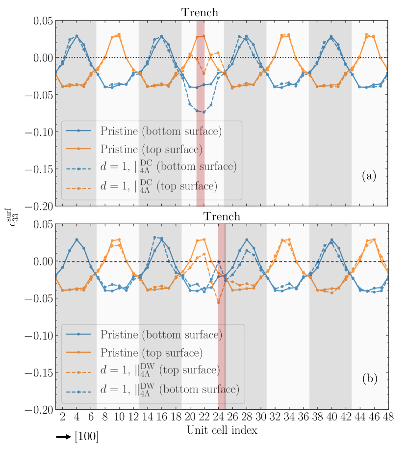
Motivated by the experimental observation of defect-induced out-of-plane negative strains [4], we examined this effect within our simulations. We define the out-of-plane surface strain relative to the average out-of-plane lattice parameter of the pristine film (4.051 Å). Negative strains emerge for all films within unit cells of the ST, weakly depending on apart from which gives rise to large negative strains further from the ST which we postulate is a fictitious artefact of the supercell geometry (the vertical trench-trench interaction is too strong as at they become separated by only a single unit cell). When increasing the ST separation to , we observe no change in the range or character of the strain field. These fields are shown in Fig. 3, overlaid with the underlying strain field of the pristine film. For the pristine film, we see that the strain fields of the upper and lower surfaces are a pair of sinusoids in antiphase with asymmetrical antinodes. The origin of this asymmetry is beyond the scope of this letter but will be addressed in a forthcoming publication. We see in Fig. 3(a) that near the ST, the ST-induced negative strain cooperates with the negative strain of the pristine film at the bottom surface (where polarization is directed along [001]) of . The positive strain of the pristine film is cancelled on the upper surface. Fig. 3(b) shows that brings slightly longer-range disorder to the surface strain field than . While these effects could contribute to the DW alignment mechanism (i.e. piezoelectric and/or flexoelectric contributions), our method does not allow us to separate these contributions from changes in the polarization emerging from the aforementioned depolarizing field minimization. We remark that direct comparison of our results with ref. [4] are limited by the drastically different length scales. In [4], defects extend over many domain periods and are less uniform than this study. It is then feasible that different mechanisms could begin to contribute. That being said, in PTO/STO systems, the in-plane axial components have been observed with much longer periods, robust throughout entire samples [40]. Then, for larger surface defects, while it may not be possible to discriminate between and arrangements, perpendicular-to-wall geometries can be precluded. So long as the defect sufficiently disturbs the axial components, the resulting depolarizing field penalty can be large enough to prevent the condensation of perpendicular-to-wall geometries and thus the ST-DW parallel alignment phenomenon is still observed.
In summary, we have investigated the mechanism for experimentally observed parallel DW-ST alignment with state-of-the art DFT simulations using as many as 5,136 atoms. We assert that although the mechanism could have many contributing components, it can be satisfactorily explained by how well the polar texture of a film can adapt to a ST with a given orientation relative to the DW. The preferred orientation features dipole moments in the vicinity of the ST in an arrangement where energy penalties from ST-induced depolarizing fields are most reduced. Subsequently, the preferred polar texture best restores polar continuity and resembles the polar texture of the pristine film. These conditions hold true for the films which we find to be the most energetically stable arrangement, independent of the presence of AFD modes, larger lateral ST separations and three depths (1, 2 and 3 unit cells). We find large negative strains in the vicinity of our STs for all films. While it is possible that this contributes to the alignment mechanism via piezoelectric and/or flexoelectric effects, we cannot decouple these from other effects within our method. ST-DW parallel alignment is only one consequence of ST engineering. Other exotic polar textures could be engineered in a wide range of ferroelectric nanostructures as demonstrated by the appearance of ST-induced polar cycloidal modulations in + AFD films. Finally, we remark that the system sizes treated within this letter greatly surpass standard ab initio studies. This demonstrates the power of DFT methods [23, 24, 25] which we expect to become widely adopted.
Acknowledgements
We are grateful for use of the ARCHER/ARCHER2 UK National Supercomputing Service funded by the UKCP consortium EPSRC Grant Ref. No. EP/P022561/1. The authors also thank Pavlo Zubko and Marios Hadjimichael for their careful review this letter.
References
- Streiffer et al. [2002] S. K. Streiffer, J. A. Eastman, D. D. Fong, C. Thompson, A. Munkholm, M. V. R. Murty, O. Auciello, G. R. Bai, and G. B. Stephenson, Phys. Rev. Lett. 89, 067601 (2002).
- Fong et al. [2004] D. D. Fong, G. B. Stephenson, S. K. Streiffer, J. A. Eastman, O. Auciello, P. H. Fuoss, and C. Thompson, Science 304, 1650 (2004).
- Thompson et al. [2008] C. Thompson, D. D. Fong, R. V. Wang, F. Jiang, S. K. Streiffer, K. Latifi, J. A. Eastman, P. H. Fuoss, and G. B. Stephenson, Appl. Phys. Lett. 93, 182901 (2008).
- Hadjimichael et al. [2018] M. Hadjimichael, E. Zatterin, S. Fernandez-Peña, S. J. Leake, and P. Zubko, Phys. Rev. Lett. 120, 037602 (2018).
- Park et al. [2018] J. Park, J. Mangeri, Q. Zhang, M. H. Yusuf, A. Pateras, M. Dawber, M. V. Holt, O. G. Heinonen, S. Nakhmanson, and P. G. Evans, Nanoscale 10, 3262 (2018).
- Seidel et al. [2009] J. Seidel, L. W. Martin, Q. He, Q. Zhan, Y.-H. Chu, A. Rother, M. E. Hawkridge, P. Maksymovych, P. Yu, M. Gajek, N. Balke, S. V. Kalinin, S. Gemming, F. Wang, G. Catalan, et al., Nat. Mater. 8, 229 (2009).
- Hong et al. [2021] Z. Hong, S. Das, C. Nelson, A. Yadav, Y. Wu, J. Junquera, L.-Q. Chen, L. W. Martin, and R. Ramesh, Nano Lett. (2021).
- Das et al. [2020] S. Das, Z. Hong, V. A. Stoica, M. A. P. Gonçalves, Y. T. Shao, E. Parsonnet, E. J. Marksz, S. Saremi, M. R. McCarter, A. Reynoso, C. J. Long, A. M. Hagerstrom, D. Meyers, V. Ravi, B. Prasad, H. Zhou, et al., Nat. Mater. (2020).
- Whyte and Gregg [2015] J. Whyte and J. Gregg, Nat. Commun. 6, 7361 (2015).
- McConville et al. [2020] J. P. V. McConville, H. Lu, B. Wang, Y. Tan, C. Cochard, M. Conroy, K. Moore, A. Harvey, U. Bangert, L.-Q. Chen, A. Gruverman, and J. M. Gregg, Adv. Funct. Mater. 30, 2000109 (2020).
- Sharma et al. [2017] P. Sharma, Q. Zhang, D. Sando, C. H. Lei, Y. Liu, J. Li, V. Nagarajan, and J. Seidel, Sci. Adv. 3, e1700512 (2017).
- Jiang et al. [2017] J. Jiang, Z. L. Bai, Z. H. Chen, L. He, D. W. Zhang, Q. H. Zhang, J. A. Shi, M. H. Park, J. F. Scott, C. S. Hwang, and A. Q. Jiang, Nat. Mater. 17, 49 (2017).
- Maksymovych et al. [2011] P. Maksymovych, A. N. Morozovska, P. Yu, E. A. Eliseev, Y.-H. Chu, R. Ramesh, A. P. Baddorf, and S. V. Kalinin, Nano Lett. 12, 209 (2011).
- Catalan et al. [2012] G. Catalan, J. Seidel, R. Ramesh, and J. F. Scott, Rev. Mod. Phys. 84, 119 (2012).
- Whyte et al. [2013] J. R. Whyte, R. G. P. McQuaid, P. Sharma, C. Canalias, J. F. Scott, A. Gruverman, and J. M. Gregg, Adv. Mater. 26, 293 (2013).
- Werner et al. [2017] C. S. Werner, S. J. Herr, K. Buse, B. Sturman, E. Soergel, C. Razzaghi, and I. Breunig, Sci. Rep. 7, 9862 (2017).
- Shimada et al. [2010a] T. Shimada, S. Tomoda, and T. Kitamura, J. Phys. Condens. Matter 22, 355901 (2010a).
- Prosandeev and Bellaiche [2007] S. Prosandeev and L. Bellaiche, Appl. Phys. Lett. 91, 072901 (2007).
- Tang et al. [2015] Y. L. Tang, Y. L. Zhu, X. L. Ma, A. Y. Borisevich, A. N. Morozovska, E. A. Eliseev, W. Y. Wang, Y. J. Wang, Y. B. Xu, Z. D. Zhang, and S. J. Pennycook, Science 348, 547 (2015).
- Baker and Bowler [2020] J. S. Baker and D. R. Bowler, Adv. Theory Simul. 3, 2000154 (2020).
- Bowler and Miyazaki [2012] D. R. Bowler and T. Miyazaki, Rep. Prog. Phys. 75, 036503 (2012).
- Goedecker [1999] S. Goedecker, Rev. Mod. Phys. 71, 1085 (1999).
- Li et al. [1993] X.-P. Li, R. W. Nunes, and D. Vanderbilt, Phys. Rev. B 47, 10891 (1993).
- Palser and Manolopoulos [1998] A. H. R. Palser and D. E. Manolopoulos, Phys. Rev. B 58, 12704 (1998).
- Bowler and Gillan [1999] D. Bowler and M. Gillan, Comput. Phys. Commun. 120, 95 (1999).
- Bowler et al. [2006] D. R. Bowler, R. Choudhury, M. J. Gillan, and T. Miyazaki, Phys. Status Solidi B 243, 989 (2006).
- Nakata et al. [2020] A. Nakata, J. S. Baker, S. Y. Mujahed, J. T. L. Poulton, S. Arapan, J. Lin, Z. Raza, S. Yadav, L. Truflandier, T. Miyazaki, and D. R. Bowler, J. Chem. Phys. 152, 164112 (2020).
- Zen [2020] CONQUEST v1.0.5 (2020).
- Torralba et al. [2008] A. S. Torralba, M. Todorović, V. Brázdová, R. Choudhury, T. Miyazaki, M. J. Gillan, and D. R. Bowler, J. Phys. Condens. Matter 20, 294206 (2008).
- Bowler et al. [2019] D. R. Bowler, J. S. Baker, J. T. L. Poulton, S. Y. Mujahed, J. Lin, S. Yadav, Z. Raza, and T. Miyazaki, Jpn. J. Appl. Phys 58, 100503 (2019).
- Baker et al. [2020] J. S. Baker, T. Miyazaki, and D. R. Bowler, Electron. Struct. 2, 025002 (2020).
- Hamann [2013] D. R. Hamann, Phys. Rev. B 88, 085117 (2013).
- van Setten et al. [2018] M. van Setten, M. Giantomassi, E. Bousquet, M. Verstraete, D. Hamann, X. Gonze, and G.-M. Rignanese, Comput. Phys. Commun. 226, 39 (2018).
- Perdew and Wang [1992] J. P. Perdew and Y. Wang, Phys. Rev. B 45, 13244 (1992).
- [35] See Supplemental Material [publisher url] for finer details of the simulation method and required preliminary tests/studies used to enable the main article, which includes Refs. [42, 43, 44, 45, 46, 47, 48, 49]. Additional raw data including basis sets and example inputs are hosted at https://doi.org/10.5281/zenodo.4699823.
- Sai et al. [2000] N. Sai, B. Meyer, and D. Vanderbilt, Phys. Rev. Lett. 84, 5636 (2000).
- Bengtsson [1999] L. Bengtsson, Phys. Rev. B 59, 12301 (1999).
- Munkholm et al. [2001] A. Munkholm, S. K. Streiffer, M. V. R. Murty, J. A. Eastman, C. Thompson, O. Auciello, L. Thompson, J. F. Moore, and G. B. Stephenson, Phys. Rev. Lett. 88, 016101 (2001).
- Resta et al. [1993] R. Resta, M. Posternak, and A. Baldereschi, Phys. Rev. Lett. 70, 1010 (1993).
- Shafer et al. [2018] P. Shafer, P. García-Fernández, P. Aguado-Puente, A. R. Damodaran, A. K. Yadav, C. T. Nelson, S.-L. Hsu, J. C. Wojdeł, J. Íñiguez, L. W. Martin, E. Arenholz, J. Junquera, and R. Ramesh, PNAS 115, 915 (2018).
- Shimada et al. [2010b] T. Shimada, S. Tomoda, and T. Kitamura, Phys. Rev. B 81, 144116 (2010b).
- Gonze et al. [2016] X. Gonze, F. Jollet, F. A. Araujo, D. Adams, B. Amadon, T. Applencourt, C. Audouze, J.-M. Beuken, J. Bieder, A. Bokhanchuk, et al., Comput. Phys. Commun. 205, 106 (2016).
- Gonze et al. [2009] X. Gonze, B. Amadon, P.-M. Anglade, J.-M. Beuken, F. Bottin, P. Boulanger, F. Bruneval, D. Caliste, R. Caracas, M. Côté, et al., Comput. Phys. Commun. 180, 2582 (2009).
- Bowler et al. [2020] D. R. Bowler, J. S. Baker, J. T. L. Poulton, S. Y. Mujahed, L. Truflandier, S. Yadav, Z. Raza, T. Miyazaki, M. Gillan, A. Nakata, et al., The CONQUEST code: public release at https://github.com/OrderN/CONQUEST-release (2020).
- Zhang et al. [2017] Y. Zhang, J. Sun, J. P. Perdew, and X. Wu, Phys. Rev. B 96, 035143 (2017).
- Vanderbilt [1990] D. Vanderbilt, Phys. Rev. B 41, 7892 (1990).
- Hotelling [1943] H. Hotelling, Ann. Math. Stat. 14, 1 (1943).
- Aguado-Puente and Junquera [2012] P. Aguado-Puente and J. Junquera, Phys. Rev. B 85, 184105 (2012).
- Pulay [1980] P. Pulay, Chem. Phys. Lett 73, 393 (1980).