eWake: A Novel Architecture for Semi-Active Wake-Up Radios Attaining Ultra-High Sensitivity at Extremely-Low Consumption
Abstract.
In this work we propose a new scheme for semi-passive Wake-Up Receiver circuits that exhibits remarkable sensitivity beyond -70 dBm, while state-of-the-art receivers illustrate sensitivity of up to -55 dBm. The receiver employs the typical principle of an envelope detector that harvests RF energy from its antenna, while it employs a nano-power operation amplifier to intensify the obtained signal prior to the final decoding that is realized with the aid of a comparator circuit. It operates at the 868 MHz ISM band using OOK signals propagated through LoRa transceivers, while also supporting addressing capabilities in order to awake only the specified network’s nodes. The power expenditure of the developed receiver is as low as 580 nA, remaining at the same power consumption levels as the state-of-the-art implementations.
1. Introduction
Energy efficiency is a leading topic of research in the domain of Wireless Sensor Networks (WSNs). In most real-world applications, sensor nodes are battery operated, while their life duration is solely dependent on the battery’s remaining charge and the node’s power profile. A common strategy for saving energy in sensor networks is the duty-cycle practice, which suggests that sensor nodes enter a low-power mode, the so-called sleep state, in order to save as much energy as possible during their inactive periods. The sleep state is interrupted by short, burst events, where sensors sense, process and propagate data. The above principle is usually realized using internal or external time keeping circuits that provide fixed interrupt signals to awake the devices from their sleep state. Moreover, it is common that the interval of the wake-up signals is fixed and predefined depending on the application scenario of the network. Despite the fact that the aforementioned principle significantly reduces the overhearing and idle listening problem, which is a major source of energy wastage (Ye and Heidemann, 2004), it is not considered to be the best practice, especially in application scenarios that do not require fixed time intervals.
Another method that eliminates the duty-cycle obstacle is the employment of a Wake-Up Receiver (WuR), presented in a few research works (Gomez et al., 2016; Magno et al., 2016; Spenza et al., 2015; Marinkovic and Popovici, 2011; Aoudia et al., 2018; Gamm et al., 2010; Kazdaridis et al., 2017a; Nintanavongsa et al., 2012). This receiver is actually an auxiliary circuit usually attached to the main sensing device in order to notify the latter to switch from its sleep to its active phase. This circuit typically draws less than 1 A in order to remain as energy efficient as possible. Usually, a semi-active WuR combines an envelope detector that is a passive circuit along with a low-power comparator circuit that is an active component. It is worth noting that the best obtained performance in semi-active WuR systems in terms of sensitivity is observed in (Magno et al., 2016) with a reported sensitivity of -55 dBm, while the receiver circuit drains 600 nA when operating in its quiescent state. The aforementioned circuits have also gain significant attention over the last years with new principles presented in (D’Addato et al., 2020; Williams et al., 2020; Sutton et al., 2015; Cabarcas et al., 2020).
In this work we leverage the existing semi-active principle and we introduce eWake, a novel enhancement that offers substantially increased sensitivity, that goes beyond -70 dBm, while the power consumption of our WuR circuit remains at the same levels.
2. Wake-Up System Implementation
In this section we present the mini-ICARUS mote that integrates a novel WuR circuit able to detect wake-up signals at up to -70 dBm, while we discuss the technical details of the mote and the developed WuR.
2.1. System Architecture
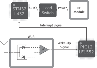
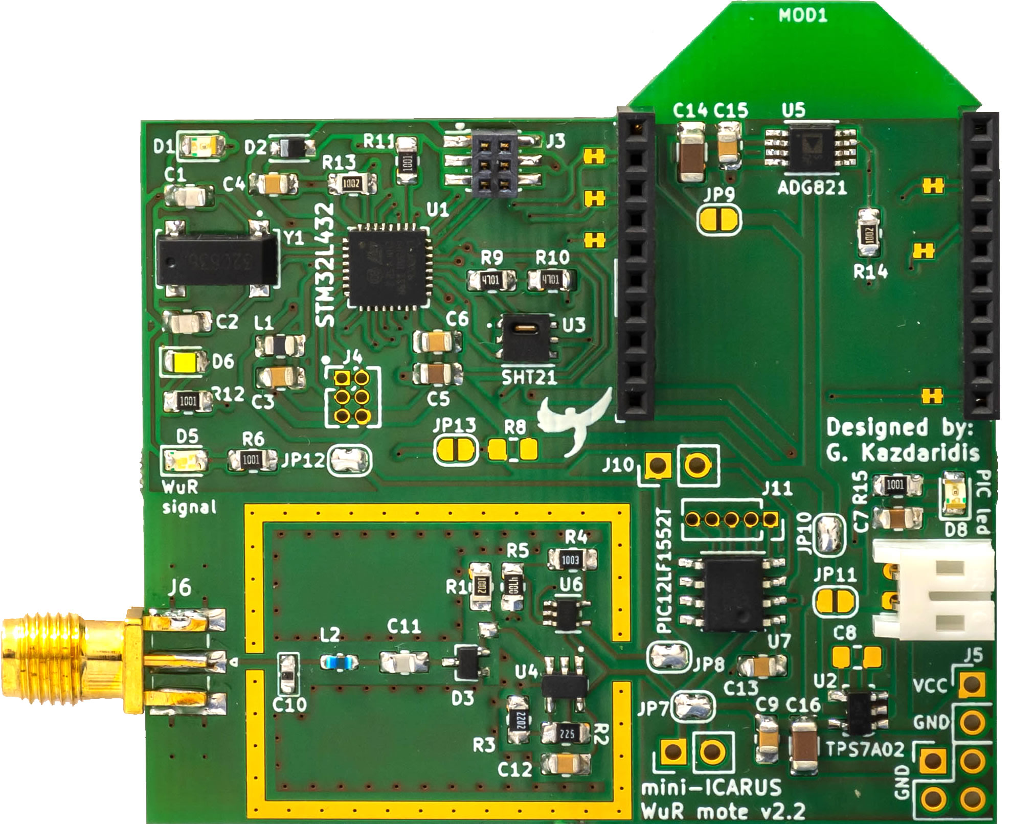
The architecture of the mini-ICARUS mote is illustrated in the Fig. 1(a), while the mote is presented in Fig. 1(b). The device integrates a novel WuR circuit, an ultra low-power microcontroller (MCU) for supporting addressing capabilities, a host MCU and an XBee footprint for plugging in wireless interfaces.
The WuR circuit is discussed in detail in next, while the low-power MCU is the 8-bit PIC12LF1552T. The PIC MCU is configured in its lowest sleep state, while it is awaken through a raising-edge Interrupt signal upon the reception of a wake-up packet. The PIC MCU process the received signal and identifies whether it should trigger the host MCU to wake-up, in case of receiving the correct wake-up packet, or to return back to the sleep phase if not. The host MCU is the STM32L432 which is an ultra low-power ARM Cortex-M4 32-bit RISC MCU operating at a frequency of up to 80 MHz. The STM32L432 remains in sleep state, consuming only 20 nA, awaiting from the PIC MCU an interrupt signal when a correct wake-up packet is received (containing the proper wake-up address). Upon the reception of such a packet the STM32L432 switches to its active state in order to measure, process and transmit data as described by the application scenario. The mini-ICARUS mote integrates an XBee footprint socket where the user can attach the desired wireless interface, such as IEEE 802.15.4 modules, LoRa transceivers or other wireless modems. Notably, wireless interfaces usually draw significant amount of power even when in sleep (Kazdaridis et al., 2020a), thus we employed a load-switch to entirely turn off the power supply of the wireless module when not in use. The aforementioned method is known as power-gating technique (Silva et al., 2012).
2.2. Wake-up Receiver Implementation
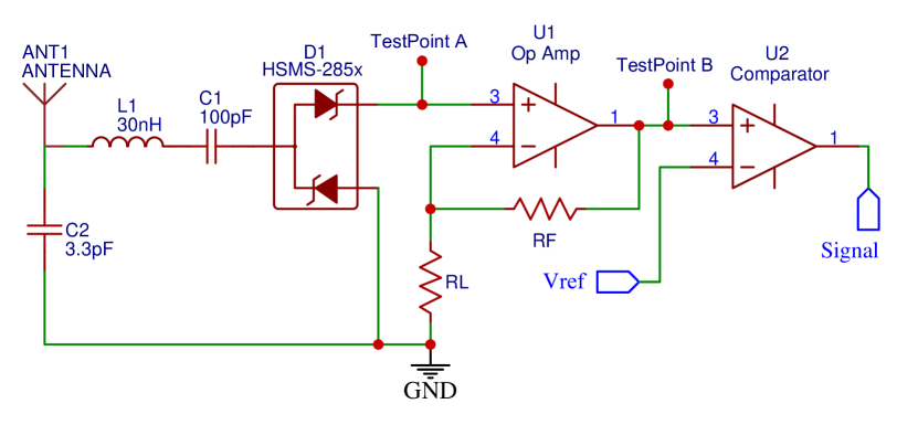
The developed prototype receiver consists of low-cost off-the-shelf electronics and a low-power micro-controller. The schematic diagram of the receiver is illustrated in Fig. 2, which is integrated into the mini-ICARUS mote. For the wake-up receiver a matching network, a passive rectifier (HSMS-285c), an Operation Amplifier and a Comparator IC (Integrated Circuit) were used. Typically, the matching network consists of a capacitor and an inductor element that together form an L-C network used to match the impedance of the antenna with the rest circuit. Then, a passive rectifier in the topology of an envelope detector is formed with the aid of two Schottky diodes, used to discard the high frequency signals and to deliver the modulated OOK signal. In our setup we used the HSMS-285c rectifier by Avago Technologies. Next, the harvested signal is processed by a low-power operation amplifier and a comparator circuit in order to fed it in binary format to the PIC12LF1552T MCU. The PIC12LF1552T MCU is responsible for processing the received signal and identifying the acquired address to verify whether it should wake-up the host node or not. To awake the network’s nodes we utilize 868 MHz LoRa radio transceivers, by modulating the propagated information using On-Off Keying (OOK) modulation.
Our finding lies in the observation that the power harvested by the envelope detector (the output signal of the HSMS-285c rectifier - TestPoint A, in Fig. 2) is not adequate to trigger the next stage when receiving high attenuated wake-up packets. Notably, in all the previously published works the harvested signal by the envelope detector (HSMS-285c) in TestPoint A is fed directly to the comparator IC, thus the overall sensitivity of the WuR is solely depended on the characteristics of the comparator being used. When using a comparator with low Input Offset Voltage (), as for example the LPV7215 (300 V ), the WuR circuit achieves high sensitivity of -55 dBm, while when employing the TLV3691 (3 mV ) the obtained sensitivity is only at -32 dBm. Of course, the power consumption of these comparators is proportional to their performance, meaning that the TLV3691 draws only 110 nA while the LPV7215 consumes roughly 580 nA. Table 1 summarizes the compelling analog comparators along with their characteristics. Notably, another crucial parameter that plays significant role in the performance of the WuR circuit, is the Input Bias Current (), which is drained by the comparator itself to bias the internal circuitry of the IC. In our work we propose a new architecture, by first amplifying the harvested RF signal (TestPoint A) and then feeding the intensified signal (TestPoint B) to a low-power comparator. Leveraging this strategy we are able to detect RF signals even when receiving highly attenuated packets, thus we achieve sensitivity far beyond the state-of-the-art. Our early experiments have illustrated sensitivity beyond -70 dBm.
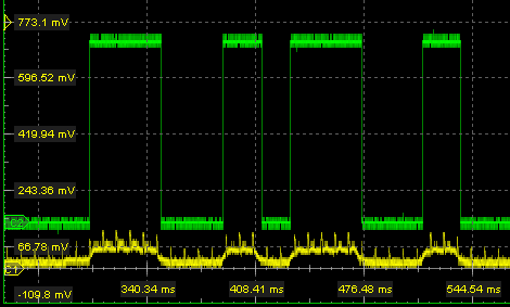
Fig. 3 illustrates the obtained signal level amplified by the operation amplifier as measured in TestPoint B with a yellow line, and the output of the comparator IC (labeled as Signal) with a green line, when receiving a wake-up packet at -60 dBm.
| Comparators | Drain | Sensitivity | ||
|---|---|---|---|---|
| TLV3691 | 110 nA | 3 mV | 80 pA | -32 dBm (Magno et al., 2016) |
| TLV7031/41 | 335 nA | 100 V | 2 pA | - |
| TLV3701 | 560 nA | 200 V | 80 pA | - |
| LPV7215 | 580 nA | 300 V | -40 fA | -55 dBm (Magno et al., 2016) |
| LTC1540 | 300 nA | n/a | 10 fA | -51 dBm (Marinkovic and Popovici, 2011) |
| MAX919 | 350 nA | 1 mV | 150 fA | - |
| TS881 | 260 nA | 500 V | 1 pA | - |
| ADCMP380 | 92 nA | n/a | 4 nA | - |
Components Selection: The Radio Frequency (RF) passive rectifier we used is the HSMS-285c which is the best option for harvesting RF signals, optimized for frequencies below 1.5 GHz. As regards the Operation Amplifier we have employed is the LPV811 that features 450 nA power draw, configured to amplify the obtained signal a hundredfold. Next the signal is fed to the comparator IC, which in our prototype is the TLV3691 that consumes roughly 120 nA. We opted for the TLV3691 in spite of featuring high , since the proposed circuit is no longer dependent on the comparator’s . The overall consumption of 525 nA can be further optimized by reducing the supply voltage from 3.3V to 1.6V.
Regarding the Operation Amplifier and the comparator ICs, there are also several other options that could be used instead. Table 2 summarizes some recently launched ICs by Texas Instruments that feature extremely low-power consumption, in the order of a few hundred nA. Notably, the majority of the general purpose operation amplifiers consume at least a few A, thus the usage of the proposed amplifiers is deemed necessary. Apparently, another very attractive option is the LPV801 amplifier that draws only 320 nA, while also featuring very low of 100 fA. In future designs we are looking into using the aforementioned amplifier to reduce the overall power consumption. By doing so, the overall consumption of the WuR circuit will be as low as 450 nA. Regarding the employed comparator, is already one of the best options (Table 2), since only the ADCMP380 IC drains lower power but it comes with a fixed voltage reference of 500 mV or 1 V, thus not that applicable in our system. Notalby, currently we use a voltage reference threshold of toughly 27 mV.
It is worth noting that all the selected components are off-the-shelf and substantially inexpensive, thus the proposed WuR can be easily implemented.
Address Matching: In order to reduce the overall false positive wake-ups as a result also the power consumption of the entire system, we employed an ultra low-power MCU that process the received signal prior triggering the host MCU. This MCU is the 8-bit PIC12LF1552T. The PIC12LF1552T is configured in sleep state, consuming only 20 nA, while it is awaken upon the reception of a wake-up frame. Notably, the PIC12LF1552T requires a few s to wake-up in order to process the signal, thus our wake-up packet contains a preamble with a similar time duration in order to be sure that the MCU is ready to read and process the required information. We selected the PIC MCU to provide address matching capabilities, because it drains only 32 A per MHz thus considered to be an extremely inexpensive solution in terms of power consumption. In our application it is configured to operate at 2 MHz, as also in most related works (Magno et al., 2016).
Matching Network: In order to tune the matching network of a WuR circuit, a network analyzer is essential since it calculates the exact values required for the L-C components employed, to transfer as much power as possible of the received radio signal available on the antenna to the rest of the circuit. This step is essential, since the only way to evaluate the sensitivity of the receiver is to execute realistic experiments with RF transmitters and of course by employing variable attenuators to precisely diminish the transmitted radio signal. However, such an apparatus is extremely expensive, therefore not easy to find and use in every laboratory. In our setup we followed a different approach to tune the matching network, by employing the low-cost ADALM-PLUTO (Module, 2021) Software Defined Radio (SDR). We used the SDR platform to transmit signals in different center frequencies in order to detect the frequency of the utilized L-C network that provides less attenuation. In essence, we plot the performance of the L-C network around the given frequency band. After repeating the same experiment by using different L-C values we identified the elements that provide the highest received signal strength in the 868 MHz band. To characterize the strength of the received signal we measured the harvested voltage output of the HSMS-285c rectifier (TestPoint A in Fig. 2) of the proposed WuR circuit. Notably, we easily approached the required L-C values by starting our trials with values similar to the ones presented in other works (Node, 2021).
| Op. Amp. | Consumption | ||
|---|---|---|---|
| LPV521 | 350 nA | 100 V | 40 fA |
| LPV801 | 320 nA | 550 V | 100 fA |
| LPV811 | 450 nA | 55 V | 100 fA |
| LPV821 | 650 nA | 1.5 V | 7 pA |
| TLV8541 | 480 nA | 300 V | 100 fA |
| TLV8801 | 450 nA | 550 V | 100 fA |
| TLV8811 | 450 nA | 75 V | 100 fA |
Transmitter Device: To awake the network’s nodes we use the LoRa (Alliance, 2021) technology, which is a low-power ultra-long range IoT technology. The wake-up packets are modulated using OOK modulation, which in essence means that carrier signal is transmitted to represent the binary one, or suspended to represent the binary zero. Of course, the signal is modulated at a fixed transmission rate, so as the receiver to be able to extract the information by the received signal. Notably, the modulated packet contains two chunks of information, the network id and the address of the targeted node. This way, the wake-up circuit, ensures firstly that the packet belongs to its wake-up network and secondly whether the address refers to it. Of course, sensor nodes, can support more than one wake-up addresses, so that we can awaken a set of nodes at the same time. It is worth noting that the wake-up signal begins with an artificial delay to allow the activation of the PIC12LF1552T MCU, prior to the reception of the modulated information.
3. Conclusions
In this work we showcase a new scheme for semi-passive WuR circuits that remarkably increases the sensitivity of the existing state-of-the-art implementations, reaching beyond -70 dBm. Our finding lies in the employment of a nano-power amplifier that intensifies the signal prior to the decoding process. The overall consumption of our proposed circuit is roughly 580 nA, while it can be substantially reduced by using alternative ICs. Lastly, our future plans include the measurement and characterization of the proposed WuR’s power consumption profile using our power monitoring tools (Kazdaridis et al., 2020b, 2017b).
References
- (1)
- Alliance (2021) Lora Alliance. [Accessed 28-March-2021]. https://goo.gl/DOR0CS.
- Aoudia et al. (2018) F. A. Aoudia, M. Gautier, M. Magno, M. Le Gentil, O. Berder, and L. Benini. 2018. Long-short range communication network leveraging LoRa™ and wake-up receiver. Microprocessors and Microsystems (2018).
- Cabarcas et al. (2020) Felix Cabarcas, Juan Aranda, and Diego Mendez. 2020. OpenWuR - An Open WSN Platform for WuR-Based Application Prototyping. In Proceedings of the 2020 International Conference on Embedded Wireless Systems and Networks on Proceedings of the 2020 International Conference on Embedded Wireless Systems and Networks (Lyon, France) (EWSN ’20). Junction Publishing, USA, 212–217.
- D’Addato et al. (2020) Matteo D’Addato, Alessio Antolini, Francesco Renzini, Alessia Maria Elgani, Luca Perilli, Eleonora Franchi Scarselli, Antonio Gnudi, Michele Magno, and Roberto Canegallo. 2020. Nanowatt Clock and Data Recovery for Ultra-Low Power Wake-Up Based Receivers. In Proceedings of the 2020 International Conference on Embedded Wireless Systems and Networks on Proceedings of the 2020 International Conference on Embedded Wireless Systems and Networks (Lyon, France) (EWSN ’20). Junction Publishing, USA.
- Gamm et al. (2010) G. U. Gamm, M. Sippel, M. Kostic, and L. M. Reindl. 2010. Low power wake-up receiver for wireless sensor nodes. In Proc. of ISSNIP ’10.
- Gomez et al. (2016) A. Gomez, L. Sigrist, M. Magno, L. Benini, and L. Thiele. 2016. Dynamic energy burst scaling for transiently powered systems. In Design, Automation Test in Europe Conf. Exhibition (DATE) ’16.
- Kazdaridis et al. (2020a) G. Kazdaridis, N. Sidiropoulos, I. Zografopoulos, P. Symeonidis, and T. Korakis. 2020a. Nano-Things: Pushing Sleep Current Consumption to the Limits in IoT Platforms. In Proceedings of the 10th International Conference on the Internet of Things (Malmö, Sweden) (IoT ’20).
- Kazdaridis et al. (2017a) G. Kazdaridis, P. Skrimponis, I. Zographopoulos, P. Symeonidis, T. Korakis, and L. Tassiulas. 2017a. Enabling Asynchronous Awakenings in Wireless Sensor Networks Towards Removing Duty-Cycle Barriers. In Proceedings of the 11th Workshop on Wireless Network Testbeds, Experimental Evaluation & CHaracterization (Snowbird, Utah, USA) (WiNTECH ’17).
- Kazdaridis et al. (2020b) G. Kazdaridis, I. Zografopoulos, N. Sidiropoulos, P. Symeonidis, and T. Korakis. 2020b. EProfiler: High-Precision Power Monitoring System for IoT Devices Featuring Extreme Dynamic Range of Operation. In Prof. of the ENSsys ’20. New York, NY, USA.
- Kazdaridis et al. (2017b) G. Kazdaridis, I. Zographopoulos, P. Symeonidis, P. Skrimponis, T. Korakis, and L. Tassiulas. 2017b. Demo: In-situ Power Consumption Meter for Sensor Networks Supporting Extreme Dynamic Range. In Proc. of WiNTECH ’17.
- Magno et al. (2016) M. Magno, V. Jelicic, B. Srbinovski, V. Bilas, E. Popovici, and L. Benini. 2016. Design, Implementation, and Performance Evaluation of a Flexible Low-Latency Nanowatt Wake-Up Radio Receiver. IEEE Transactions on Industrial Informatics (2016).
- Marinkovic and Popovici (2011) S. J. Marinkovic and E. M. Popovici. 2011. Nano-Power Wireless Wake-Up Receiver With Serial Peripheral Interface. IEEE Journal on Selected Areas in Communications (2011).
- Module (2021) ADALM-PLUTO Software-Defined Radio Active Learning Module. [Accessed 28-March-2021]. https://www.analog.com/en/design-center/evaluation-hardware-and-software/evaluation-boards-kits/adalm-pluto.html.
- Nintanavongsa et al. (2012) P. Nintanavongsa, U. Muncuk, D. R. Lewis, and K. R. Chowdhury. 2012. Design Optimization and Implementation for RF Energy Harvesting Circuits. IEEE Journal on Emerging and Selected Topics in Circuits and Systems 2, 1 (2012), 24–33. https://doi.org/10.1109/JETCAS.2012.2187106
- Node (2021) Akos Pasztor. WuLoRa: Energy-Efficient IoT Sensor Node. [Accessed 28-March-2021]. https://akospasztor.com/projects/wulora/report.pdf.
- Silva et al. (2012) A. Silva, M. Liu, and M. Moghaddam. 2012. Power-Management Techniques for Wireless Sensor Networks and Similar Low-Power Communication Devices Based on Nonrechargeable Batteries. Journal of Comp. Networks and Com. (2012).
- Spenza et al. (2015) D. Spenza, M. Magno, S. Basagni, L. Benini, M. Paoli, and C. Petrioli. 2015. Beyond duty cycling: Wake-up radio with selective awakenings for long-lived wireless sensing systems. In In Proc. of INFOCOM ’15.
- Sutton et al. (2015) Felix Sutton, Bernhard Buchli, Jan Beutel, and Lothar Thiele. 2015. Zippy: On-Demand Network Flooding. In Proceedings of the 13th ACM Conference on Embedded Networked Sensor Systems (Seoul, South Korea) (SenSys ’15). Association for Computing Machinery, New York, NY, USA. https://doi.org/10.1145/2809695.2809705
- Williams et al. (2020) J. M. Williams, R. Khanna, Y. Qian, and H. Liu. 2020. Proof-of-Concept for an IoT Sensor Platform with 2.4GHz Wake-up Radio. In 2020 IEEE Radio and Wireless Symposium (RWS). 239–242. https://doi.org/10.1109/RWS45077.2020.9050096
- Ye and Heidemann (2004) Wei Ye and John Heidemann. 2004. Wireless Sensor Networks. Kluwer Academic Publishers, Norwell, MA, USA, Chapter Medium Access Control in WSNs.