First Principles Calculations for Topological Quantum Materials
Abstract
Discoveries of topological states and topological materials reshape our understanding of physics and materials over the last 15 years. First-principles calculations have been playing a significant role in bridging the theory of topology and experiments by predicting realistic topological materials. In this article, we overview the first-principles methodology on topological quantum materials. First, we unify different concepts of topological states in the same band inversion scenario. Then, we discuss the topology using first-principles band structures and newly-established topological materials databases. We stress challenges in characterizing symmetry-independent Weyl semimetals and calculating topological surface states, closing with an outlook on the exciting transport and optical phenomena induced by the topology.
H1 Introduction
Over the past decades, first-principles materials calculations have been playing a significant role in bridging fundamental theory and experiments. In particular, this has impacted the field of topological materials. For example, the last decade witnessed the successful prediction of the Bi2Se3-family of topological insulators (TIs) [1, 2], the SnTe-class of topological crystalline insulators (TCIs) [3] and the TaAs-family of Weyl semimetals (WSMs) [4, 5], stimulating the rapid development of this field. Assisted by the prediction power of first-principles calculations on weakly-interacting systems, theory usually leads the experimental research in topological materials, which is rare in the field of condensed-matter physics.
Guided by the topological classifications, first-principles calculations identify topological materials by computing the bulk topological invariants (for example, the index characterized by the parity for TIs [6] ) and the topological surface states (TSSs). Then related materials can be synthesized and characterized usually by measuring TSSs via angle-resolved photoemsission spectroscopy [7, 8] or scanning tunneling microscopy [9, 10]. Topological band theory, first-principles calculations, materials preparation, and materials measurement cooperate intimately in a back-and-forth way as the materials design. In this Review, first-principles calculations mainly refer to the density-functional theory (DFT) [11] and DFT-derived effective models such as the localized Wannier functions [12]. Studies on topological systems also push today’s first-principles calculations to pay more attention to the consequences of the time-reversal symmetry (TRS) and crystalline symmetries on the band structure than before.
There are many excellent reviews on the general topological states, topological materials [13, 14, 15, 16, 17, 18, 19, 20, 21, 22, 23, 24, 25, 26, 27, 28, 29, 30], and related first-principles calculations [31, 32, 33, 34, 35, 36]. This Technical Review aims to overview the state-of-the-art first-principles methodology and provide a beginner’s guide in the study of topological materials. First, we heuristically unify different topological states in the same band inversion scenario and then demonstrate the TSSs by the bulk-boundary correspondence. Second, we introduce the topological invariants and symmetry indicators, which distinguishes a topological state from atomic insulators. Next, we present the general first-principles procedure to extract the bulk topology and compute TSSs by representative topological materials, including TIs[37, 38, 39, 40], topological crystalline insulators (TCIs) [41], Dirac semimetals (DSMs) [42, 43], Weyl semimetals (WSMs), [44, 45, 46] nodal line semimetals (NLSMs) [47, 48] and higher-order topological insulators (HOTIs) [49, 50, 51, 52, 53]. We focus on weakly interacting topological materials in this Review as first-calculations are limited in their ability to handle strongly-correlated systems. In addition, we provide tutorial documents for all examples in supplementary information (SI).
H1 Topological band theory
Band theory was a seminal success in applying quantum mechanics to solid materials. After nearly a century, it is incredible to discover qualitatively new phenomena in this field. The TI is such a case, which is characterized by the robust metallic surface states inside the bulk energy gap. The TI band structure is intuitively characterized by a band inversion [39] — in which the valence and conduction bands switch order compared to an ordinary insulator. Up to our knowledge, William Shockley [54] first pointed out that band inversion leads to unique states on the surface by a spinless model. The Shockley surface states represent charge polarization, which is sensitive to changes in the surface potential. Further, a band inversion leads to the gapless bulk phase in the 2D or 3D spinless model without spin-orbital coupling (SOC). Thus, the Shockley state was debated and ignored as time passed (see REF. 55 for an overview). In 2006, band inversion and SOC were combined to propose a TI, which was then experimentally realised in HgTe/CdTe quantum wells [39]. To be accurate, the band inversion refers to the order change between the valence and conduction bands with opposite parities [6]. In the absence of well-defined parities (such as inversion symmetry-breaking), we consider the band inversion a heuristic scenario by assuming that the inversion-breaking bands are adiabatically connected to inversion symmetric states [14, 13]. In the following discussions, we assume a 3D system with the TRS and include SOC unless otherwise specified.
H2 Bulk-boundary correspondence and TIs
Consider a normal insulator and a TI, which exhibit opposite band orders at the center of the Brillouin zone (Fig. 1). To move smoothly from one material to the other, the band gap needs to close at the interface because of the band inversion. Therefore, the interface exhibits gapless boundary states. We can naively classify all insulators into two classes, with and without the band inversion, and consider the existence of metallic states at the interface. A normal insulator is not necessarily metallic on the surface, for example, if it is interfaced with a vacuum (approximated to be a normal insulator too). In contrast, a TI is always metallic on its surfaces. Such an argument only requires bulk band inversion and is robust against the surface perturbations such as defects or atomic reconstructions. Therefore, the band inversion in bulk dictates the existence of metallic states, the TSSs, on the boundary, which is usually called the bulk-boundary correspondence [56, 57]. The TI surface states usually form a single Dirac cone inside the bulk gap and connect the bulk valence and conduction bands. The Dirac point is protected by the TRS, which induces double spin-degeneracy called the Kramers degeneracy. Therefore, it is not surprising that TRS also defines the -type topological invariant of the bulk states. Furthermore, the bulk-boundary correspondence determines both the existence and the dispersion profile of TSSs. The adiabatic charge pumping in the bulk, which can be evaluated by the Wannier charge center evolution or Wilson loop method [58, 59, 60, 31], is actually a continuous deformation of the surface band structure [61, 62]. We take a 2D insulator as an example in Fig. 2. Because of the periodicity, we can consider the line as a loop () in the Brillouin zone (from 0 to 1 in the unit of reciprocal lattice vector) for given . For a single occupied band (Fig. 2a), the Berry phase (divided by ) acquired around the loop represents the Wannier charge center of the Bloch wave function, such that
where is the Berry connection. As varies from 0 to 1, the profile corresponds to the charge pumping along the axis, which is called parallel transport of Wannier charge centers. In the case of many valence bands, the matrix representation of parallel transport is called a Wilson loop, and its eigenspectrum () comprises the non-Abelian Berry phase factors. If shifts from one unit-cell to another in this process, it indicates a Chern insulator with Chern number . One can also observe the nontrivial winding of in the cylinder coordinate (Fig. 2b). The nontrivial charge pumping along indicates the existence of edge state when truncating the axis, because the pumping induces charge accumulation/depletion on the edge. The Wannier charge center evolution (Fig. 2c) is adiabatically connected to the corresponding edge band structure (Fig.. 2e). For a TRS-insulator, includes Kramer pairs (Fig. 2d) because of TRS and are degenerate at time-reversal-invariant momenta (TRIM) . For a normal insulator, the Kramers pair remain the same partners between neighboring TRIM. For a TI, however, the Kramers pair exchange their partners with the pair from another unit cells, displaying the same topology as their edge states (Fig. 2f). Such a correspondence between the bulk Wilson loop and boundary states will be demonstrated for different topological phases in the following sections.
H2 TCIs and HOTIs.
The bulk-boundary correspondence indicates that one band inversion leads to one surface Dirac cone when projecting the inverted bulk bands to the surface. If an odd number of band inversions occur, the TRS can protect the Dirac states. If an even number of band inversions exist, only the TRS is not enough to preserve them. We may need the crystal symmetries or their combined symmetry with TRS for protection, leading to the topological crystalline insulators (TCIs). Take a mirror-protected TCI for example (Fig. 3). Double band inversions give rise to double surface Dirac cones that cross with each other. Two Dirac cones are thus hybridized and gapped out in generic -points except two points (black dots in Fig. 1) in the mirror plane. Only the surfaces that preserve the mirror symmetry are still metallic, while surfaces without mirror symmetry are insulating. When surfaces do not preserve the mirror symmetry, the hinge between two such surfaces could be still mirror-symmetric. And on the hinge one can expect protected hinge states (see FIG. 3). This is an example of the mirror-protected HOTI [3]. The bulk and surface states for TCIs and HOTIs are illustrated in Fig. 3, which is closely related to the crystal symmetry. Generally, there are seven kinds of topological invariants associated with crystal symmetries, including translation, mirror, glide, rotation, screw, inversion, and in 230 space groups (SGs) [63, 64], resulting in the diverse TCI/HOTI phases in Fig. 3.
H2 Topological semimetals
The inverted valence and conduction bands are usually degenerate at the crossing points if SOC is turned off or negligibly small. These degenerate points are called nodal points. If they form lines or rings, they are referred to as nodal lines or nodal rings (Fig. 1b). If SOC gaps all crossing points, we obtain topologically insulating phases discussed above. Even with SOC, some individual points or lines may remain degenerate. Thus, topological semimetals refer to the gapless bulk states with SOC and mainly include the DSM, WSM, and NLSM. Because of the lack of a bulk gap to isolate the valence bands, topological invariants for topological semimetals are not well defined here. However, we can still expect special surface states, because topological semimetals usually originate from the band inversion. Especially for a WSM, TSSs form open arcs connecting Weyl points with opposite chirality on the Fermi surface[44], different from closed Fermi loops or extended Fermi lines for any other 2D states, as illustrated in Fig. 3.
H1 Symmetry indicators
The band inversion is a heuristic scenario to understand bulk topology and the corresponding TSSs. To identify the topological phase accurately, we need the information of the wave functions in the momentum space. Compared to the direct calculation of topological invariants, the symmetry indicator [65, 66, 67, 68] provides a convenient way to probe the band topology from the wave function symmetry. The symmetry indicator only requires the information of the band representations [69, 70, 71, 72] at high-symmetry momenta and can be easily implemented into first-principles calculations for real materials [73, 74, 75]. Such a symmetry approach was epitomized by the Fu-Kane parity criterion [6] to determine TIs with the inversion eigenvalues and recently generalized to all space group symmetries [65, 66, 67, 68]. The insight behind the symmetry indicator is that occupied states of the topological phase cannot be represented by symmetrical localized Wannier orbitals [59], distinct from atomic insulators (AIs). The band representation, which is based on the wave function symmetry, provides a tool to extract the symmetry indicator and identify the equivalence or distinction between a band insulator and AIs.
Generally, the symmetry data for any given band structure (occupied bands) is written as a vector (not a true vector but has the linear structure) [76]. Its elements include the number of valence bands and the number of each irreducible representation (irrep) at each high-symmetry point. These elements are constrained by the fixed electron filling and the high-symmetry lines in each space group (SG), known as the compatibility relation [77, 78, 79, 65, 66, 68]. For the gapless case, the vector violates the compatibility relation, which indicates the existence of topological semimetals with band crossings at high-symmetry points/lines. For the gapped case (with no band crossing at high-symmetry points/lines), all the vectors satisfy the linear compatibility relations and form a linear space, denoted as , which includes both gapped trivial and nontrivial symmetry entries. On the other hand, to construct the space of AIs, a set of localized symmetric Wannier orbitals are placed at Wyckoff sites, which form a set of AIs [76, 80]. With the real space description, the corresponding vectors in the momentum space are retrieved by the Fourier transform. They also form a linear space, denoted as as the for an atomic insulator, containing all the trivial symmetry entries. When subtracting from the general , by solving the quotient group mathematically, it leads to the symmetry indicator group.
The symmetry indicator group is usually generated by several and describes the mismatch of band representations between topological insulators and AIs. The nontrivial symmetry indicator value indicates the topology. For a given band structure, we can always express the vector by a linear superposition of AI basis [76]. If the coefficients are integral (fractional), the band structure is trivial (nontrivial), and the symmetry indicator value can be derived based on the coefficients. We provide an example of the wallpaper group in the supplementary information (SI) to illustrate the above concepts and procedures. Since the symmetry indicator only relies on the band representation at high-symmetry points, the symmetry indicator can be calculated in a similar way like the Fu-Kane parity criterion [63, 64]. For the 230 SGs, formalism is derived to map symmetry indicators to topological invariants.
Take SG 2 with inversion symmetry as an example. The Fu-Kane invariants () are determined by the inversion eigenvalues of all occupied Kramers pairs at TRIM , which is . For example, the strong TI index is determined by
In the symmetry indicator scheme, is expressed by (), where () represents the number of occupied even(odd)-parity states at . is even because of the Kramers degeneracy. The corresponding symmetry indicator group is . The type indicator is
One can recognize mod 2, by
where is an even constant at all 8 points. Because it is mod 4, contains more information than . For instance, indicates the existence of a TCI. Three type indicators () correspond to three weak invariants () and are expressed as
where is in unit of reciprocal lattice vectors.
Technically, some useful tools (see TABLE I) can analyze the wave functions given by DFT, generate band representations, and compute symmetry indicators [81, 73, 82]. Based on these methods, topological materials databases have been established, giving the symmetry indicator classification for known solid materials. For instance, SnTe (SG 225) has the symmetry indicator group and the indicator is , suggesting a TI/TCI. Except for SG 174 and 187-190, the largest order indicator, like the type indicator in SG 225, and type in SG 2, is called the strong factor [63, 64]. The odd value of the strong factor indicates a strong TI, while the even value corresponds to a TCI. Therefore, SnTe is a TCI. As shown in SI, the in SG 225 corresponds to two possible collections of invariants, because symmetry indicators alone cannot fully determine what kind of TCI it belongs to. One set of invariants has the nontrivial mirror Chern number [83, 3] on the (110) plane while the other set does not. By calculating the mirror Chern number, a mirror Chern insulator (the former set) is recognized for SnTe. Another example is Bi with SG 166. The symmetry indicator group is , and the indicator is (0002), belonging to a TCI. The (0002) value corresponds to two collections of invariants. By calculating the mirror Chern number of the plane, the nontrivial inversion, rotation and screw invariant can be identified. Generally, we can probe the band topology by calculating symmetry indicators and map them to a collection of invariants. Although such mapping is one to many, some specific invariant such as the mirror Chern number can help to identify the correct collection. With invariants, surface and hinge states can be anticipated according to the bulk-boundary correspondence and revealed by first-principles calculations.
The present symmetry indicator theories and databases commonly work for nonmagnetic topological materials with even electron fillings, and cannot capture the band topology at generic momenta. Thus, symmetry indicators usually cannot describe the WSM phase, although it indeed identifies WSMs in some special cases like WSMs with the inversion symmetry [84, 85] or the symmetry [86]. Further, symmetry indicators, by definition, are indicators rather than topological invariants. Even if the symmetry indicator is trivial, the system may possess hidden topology that cannot be discerned by band representations, for example, a TI in SG with no extra symmetry except the identity. Additionally, topological classifications of magnetic SGs are developed [87, 88], and a preliminary materials database is built very recently [89].
H1 Topological Materials
H2 Topological Insulators
Band structures of various TIs are shown in Fig. 4. To judge a TI by the band inversion, it is useful to compare band structures with and without SOC. For the presence of SOC, the topological invariant can be defined based on the TRS operator of the spinful fermion [37]. Without SOC, the TRS operator becomes in the spinless case, and we only get either trivial insulators or semimetals/metals. For example, Bi2Se3 is a trivial insulator without SOC and exhibits a band inversion when the SOC is tuned from zero to the experimental value, representing a topological phase transition from an ordinary insulator to a TI [1]. In the state-of-art DFT packages, the SOC amplitude can be easily tuned by a scaling parameter[90]. In addition, strain can also be applied to examine the band inversion and topological phase transition in calculations.
To identify a TI accurately, the parity criteria [6], based on the first-principles Bloch wave functions, is extensively used for insulators with the inversion symmetry. For an AI described by one symmetrical localized orbital with no dispersion, Bloch wave functions exhibit the same parity at all TRIM, leading to parity product . Other AIs are adiabatically connected to this extreme case, although parities at different TRIM may differ trivially. If the band inversion occurs once by switching the conduction and valence band at some TRIM, the parity product switches from to , generating a TI with .
The Bi2Se3 family of TIs is a well-known example to demonstrate the parity criteria. We note that graphene can also be recognized as a TI (including SOC) from the band inversion and parity. The TRIM in the 2D Brillouin zone are and points. Although it was extensively studied with the Dirac model near the -point, between the and points (Fig. 4a), we can find a clear order switching of two bands with opposite parities, also resulting in a TI. In addition, such a band inversion generates the Dirac cone at in the absence of SOC.
The TSS of a TI is characterized by an odd number of Dirac cones at the surface TRIM. The TSS calculation is usually based on two schemes: first-principles DFT calculations and tight-binding calculations. First-principles DFT calculations simulate the surface with a slab model, which is compatible with the periodic boundary condition. The slab model should be thick enough to suppress hybridization between the top and bottom surfaces, which increases the computational cost dramatically. Tight-binding calculations, which usually use Wannier function parameters extracted from DFT bulk calculations, can efficiently calculate the half-infinite surface with the iterative Green’s functions [91, 92, 93]. However, the first-principles calculations can capture the surface atomic relaxation and charge redistribution, and are usually more realistic to compare with experiments. Regardless, the surface states from different methods should provide the same topology. For instance, the surface Dirac cones from two methods are almost identical for Bi2Se3 (Fig. 4c) because Bi2Se3 exhibits the smooth van der Waals type termination with negligible surface charge redistribution compared to the bulk.
Materials without inversion symmetry and without van der Waals layered structures are more complicated. We take the half-Heusler compound LuPtBi [94, 95] for example. As shown in the inset of Fig. 4d, Pt and Bi form a zincblende lattice, and Lu fills the center position of the zincblende cube. Thus, LuPtBi exhibits strong chemical bonds and breaks the inversion symmetry. Around the point, there is an inversion between the and bands (similar to the case of HgTe [39, 6]). Because is four-fold degenerate, the band structure is gapless (even with SOC) at the Fermi level. However, there is a direct energy gap above , which is relevant to the band inversion. This gap enables us to use a more general method, the Wannier charge center evolution or Wilson loop [58, 59, 60, 31], to determine the topology. The Wilson loop method traces the Wannier charge center (Berry phase) evolution of valence wave functions between TRIM.
Fig. 4d presents the Wilson loop when taking band and below as valance bands. From to ( from 0 to ), the Wannier centers with respect to the integration loop from 0 () to () exhibit a nontrivial pattern like Fig. 2d(left), where are reciprocal lattice vectors. At and , the Wannier centers are doubly degenerate as Kramers pairs. However, Wannier centers change their Kramers partners between and , as a consequence of the band inversion. For a trivial insulator, Wannier centers still recombine with the same partners between TRIM (Fig. 2d). The Wilson loop also has the same topology as the dispersion of TSSs [62]. Results in Fig. 4d thus dictates the existence of Dirac surface states inside the gap between and .
To calculate the TSS of LuPtBi, the (111) surface is cleaved and has two possible terminations by Lu or Bi atoms. Both DFT and tight-binding calculations demonstrate the Dirac-cone-type TSSs at –0.5 eV in the inverted gap for both terminations. The tight-binding results are easier to recognize the topology since they ignore the trivial states. However, when comparing with experiments, first-principles results are more reliable to reveal the detailed dispersion of TSSs and other surface states [96]. The example of LuPtBi thus indicates that metallic bulk materials can also exhibit the nontrivial topology, and TSSs may appear far from the charge neutral point. For instance, TSSs were recognized on the surfaces of noble metals (also known as Shockley states) [97], grey arsenic [98], and in the empty states of BaBiO3 [99].
H2 Topological Crystalline Insulators
TCIs, including HOTIs, refer to topological phases with even band inversions protected by crystalline symmetries. The bulk topology only features topological surface and/or hinge states on suitable terminations. We assume the TRS in the following discussions, although some TCIs and HOTIs break TRS. The first theoretically-predicted TCI is SnTe, protected by the mirror symmetry [3]. Driven by SOC, band inversions happen four times at four points, where the Sn- and Te- states are inverted (Fig. 5a). The and each equivalent mirror plane host two points and the double band inversion inside gives the nontrivial mirror Chern number . is defined as , where is the Chern number of the mirror eigenstate with eigenvalue [83, 3]. The mirror protection can be intuitively interpreted as two copies of Chern insulators in the subspace of the mirror, whose surface states can never be hybridized. Furthermore, means two pairs of helical edge states on the boundary of (110) mirror planes. In contrast, (001) mirror planes are trivial with , since there is no band inversion inside this plane.
The Wilson loop method can demonstrate the nontrivial mirror Chern number. In both (110) and () mirror planes, Wilson loop shows two chiral modes, which are upwards and downwards flows for along (Fig. 5b), in each mirror eigenstate subspace. Therefore, it means and . In the language of symmetry indicators, SnTe has the indicator , which is mapped into the first collection of invariants shown in the SI. also gives for (110) mirror planes and other compatible invariants associated with the rotation and screw symmetry.
Because of the bulk topology, the TSS on suitable terminations can be expected for SnTe. For the (001) surface, it is normal to and mirror planes, which are projected into - and - in the surface Brillouin zone (Fig. 5a). For the (110) mirror, two L points ( and ) inside are projected into same point. Thus, two surface Dirac cones are hybridized with each other and only remain gapless along the (110) mirror projected line. Such surface topology is reflected in the (110) Wilson loop: the [001] integration loop corresponds to the (001) surface termination and the dispersion along (i.e., -- in the surface Brillouin Zone) shares the similar topology with the TSS. Overall, the (001) surface hosts four Dirac cones on the four equivalent - lines. Since Dirac cones are related by , this scenario further satisfies the nontrivial [001] rotation invariant. Generally, the surface states of each invariant are compatible with each other. Similarly, the (111) surface is normal to three mirror planes , and , which are projected into three equivalent - lines. For each mirror plane, two L points inside are projected into and (Fig. 5a). Therefore, the scenario for the (111) surface is four Dirac cones sitting at one and three points, respectively. This is consistent with the bulk Wilson loop. If the integration loop is along [111] and the acquired Berry phase disperses in the direction (which is the -- line in the surface Brillouin Zone), the Wilson loop can correspond to the (111) TSSs (Fig. 5b).
H2 Higher order topological insulators
For a mirror TCI, if the nontrivial mirror plane is not normal to side surfaces but passes through the hinge, all the surface states are gapped out. However, helical hinge states arise in the mirror-projected lines (Fig. 5c). This type of TCI belongs to the HOTI phase [3, 49, 50, 51, 52, 53]. To demonstrate this scenario, we choose the [001] as the hinge direction and (100) and (010) as side surfaces. By using the tight-binding model with the uniaxial [110] strain, as suggested in REF. 3, 53, side surfaces are gapped out while two nontrivial mirror planes (110) and survive, passing through two hinges. The Green’s function method is applied, and the system is considered as finite in the [100] direction, half-infinite in the [010] direction and periodic in the [001] direction (the hinge direction). Two hinge states can be observed in Fig. 5c, protected by (110) and mirror planes. It also satisfies the relation for the mirror protected hinge with TRS, where is the number of Kramers pairs of hinge states and is the corresponding mirror Chern number [53].
Another TCI/HOTI example is the element Bi [100, 101]. To reveal the band inversions, the parity eigenvalues at the TRIM points are shown in Fig. 5d. At , all parity eigenvalues are “+” for the top three valence bands. In contrast, all other TRIM () have two “–” and one “+”. Thus, Bi has double band inversions at the point [101]. The crystal symmetries, including the inversion and the [100] rotation (along the -axis in the hexagonal plane), define the topology of the double band inversion. Unlike mirror Chern number, topological invariants associated with rotation symmetries are difficult to calculate [50, 102]. Fortunately, using symmetry indicators greatly simplifies this process. Bi possesses the nontrivial , and . We focus on the rotation invariant , which dictates a pair of Dirac points on the () surface with the symmetry. In this plane, two band inversions lead to two surface Dirac cones at the point. Two Dirac cones cross each other in the plane and gap out by hybridization except at two crossing points that are protected by . But these two points are not necessarily high-symmetric momenta in the surface Brillouin zone [102]. Additionally, similar double band inversions also lead to the HOTI and related TSSs in -MoTe2 [103, 76], which is protected by the screw rotation.
To identify the TSS of , we cleave the surface and search the surface Brillouin zone based on the tight-binding calculations. Two Dirac cones are found in Fig. 5e, and the corresponding Wilson loop shows the same topology. The also dictates two helical hinge states on side hinges, which connect double Dirac cones on top and bottom. Unlike the mirror HOTI, the hinge states are unpinned and depend on the geometry of the sample [102, 101]. Using the same method as that for SnTe (Fig. 5c), we calculated the hinge states in Fig. 5f, which are further compatible with the inversion invariant [100] and the screw rotation invariant . However, it is technically challenging to unambiguously address the hinge states of Bi [100, 104], because neither the bulk nor side surfaces exhibit a global band gap, as indicated in Fig. 5f.
H2 Weyl Semimetals
The WSM is a 3D topological semimetal phase without requiring any symmetry protection. Instead, it needs to break either the TRS or inversion symmetry (or both) to lift the spin degeneracy, because the coexistence of TRS and inversion symmetry forces the spin degeneracy at all -points. A WSM features two-fold-degenerate accidental-crossing points, called Weyl points, between conduction and valence bands. Weyl points exhibit monopole-like Berry curvature distribution [105] and always come in pairs with opposite chiralities. Because Weyl points occur at generic momenta, addressing Weyl points and induced Fermi arc surface states [44] are technically challenging in calculations. In the following, we focus on WSM with TRS, where the symmetry indicator method usually cannot be applied (Fig. 6).
We take TaP as an example. TaP, with SG 109, is a nonmagnetic WSM without inversion symmetry [5, 4]. It contains two mirror planes and , which are related to each other by the rotation. In the plane, the bulk band structure exhibits a clear inversion from to , to in the nearby Brillouin zone (Fig. 6a). Without SOC, the band inversion induces two nodal rings in plane and another two in the plane in the first Brillouin zone. As SOC is turned on, we expect to find Weyl points near the nodal ring regimes, because other regimes are fully gapped. As shown in Fig. 6b, the nodal rings inside the planes are gapped out by SOC. Each original nodal ring evolves into three pairs of Weyl points near it, leading to twelve pairs of Weyl points in total. By searching for band crossing points near the nodal rings, Weyl points can be located. As long as one Weyl point is found at , other Weyl points can be located at and by considering the , , and TRS.
In numerical calculations, it is usually difficult to distinguish a band crossing from a small finite gap. This problem can be solved by the monopole nature of Weyl points. Weyl points feature the source ( chirality) and sink ( chirality) of Berry curvature [106], which can be calculated based on the Wannier-function Hamiltonian (see Eq. 1). Thus, the Berry curvature flux for a closed surface surrounding a Weyl point is , where represents the chirality. To estimate the Berry flux, alternatively, the Wilson loop method is equivalent but more convenient than integrating the Berry flux. On the spherical surface embodying a Weyl point, the Wilson loop could be chosen as azimuthal rings. The Berry phase of valence bands evolves from the south pole to the north pole and presents the nontrivial Chern number , as shown in Fig. 6b.
The bulk Weyl points dictate the existence of surface Fermi arcs. However, when topological Fermi arcs and trivial surface states coexist, identifying Fermi arcs is challenging. For example, TaP has multiple pairs of Weyl points and thus multiple Fermi arcs connecting them. The surfaces are also terminated by P or Ta dangling bonds, leading to trivial states. Different surface terminations naturally exhibit different surface band structures that share the same topology. Furthermore, different computation methods (DFT and tight-binding) may give different surface states that should share the same topology [4, 107, 108, 109, 110].
Topological information of bulk mirror planes is helpful to understand surface state topology. The Wilson loops in FIG. 6c reveal their topological feature. Because of TRS, the and planes are actually 2D TIs. In contrast, two diagonal glide mirror planes ( and ) are trivial 2D insulators, because the Wannier charge centers keep the same partners between and points.
The and planes are further projected to the surface - and - lines, respectively. The 2D TI of leads to odd pairs of helical edge states along the - line. In contrast, the trivial TI of leads to even pairs of helical edge states along the -. Therefore, there might be odd pairs of Fermi arcs crossing the - but stopping somewhere before the -. Indeed, FIG. 6d shows three surface states (point 1-3) between and but no state between and at the Fermi surface. In other words, the Fermi arcs can be considered as the extended edge states of the 2D TI (TRS-preserving) or the Chern insulator (TRS-breaking), as demonstrated in Fig. 2.
Since Fermi arcs connect Weyl points with opposite chiralities, we can also choose a closed loop in the surface Brillouin zone to identify the topology. If the closed loop contains the net odd chirality, there must be an odd number of Fermi cuts across the loop. Otherwise, there must be an even number of cuts. For instance, for the closed --- loop in FIG. 6e, it contains two positive W2 points (projected into the same point on the (001) surface) and one negative W1 point, with the net chirality . Fermi cuts across this loop are calculated to be five times (points 1-5 in FIG. 6d-e), as expected. The situation is also similar for the --- loop. If the surface boundary conditions are changed, the Fermi arcs may evolve dramatically [110, 111]. Despite the complexity, the surface topology can still be identified by applying the bulk-boundary correspondence.
WSMs have also attracted extensive studies in magneto-transport on the extremely large magnetoresistance [112] and the chiral anomaly effect [113] characterized by the negative magnetoresistance [114, 115, 116]. The 3D Fermi surface, especially energies of Weyl points with respect to the chemical potential, is essential to interpret experiments and exclude other effects like the current jetting [117, 118, 119]. The Fermi surface can be directly calculated from the first-principles or related tight-binding calculations. The extreme cross-section () of the Fermi surface corresponds to the basic frequency () of the quantum oscillations in experiments, by Onsager’s relation , where is the magnetic flux quantum. We can compare the angle-dependent quantum oscillations and the angle-dependent Fermi surface cross-sections, to determine the exact Fermi surface topology of WSMs [120, 121, 117].
H2 Dirac Semimetals
DSMs can be classified into band inversion-induced [43, 122] and symmetry-enforced DSMs [42]. The first type is unified in the band inversion scenario and can be viewed as two pairs of WSM: two Weyl points with opposite chiralities overlap and form the four-fold degenerate Dirac point. To maintain the band crossing, it requires the rotation symmetry (, n = 3, 4 or 6) protection. Two Dirac points sit on the rotation axis, and they cannot be gapped due to different symmetry representations of inverted bands. Generally, to check the symmetry protected band crossings, we can calculate the symmetry representations of crossing bands from first-principles. If they belong to different representations, their hybridization is forbidden. To identify the topology of DSM, we can similarly calculate the number of the 2D plane (for example, ) between Dirac points, in which the band gap is inverted. On the surface, the helical edge states of the 2D TI layer evolve into a pair of Fermi arcs. Two arcs meet each other at the projected Dirac points. The DSM can also transform into other phases by symmetry breaking. If a Dirac point picks up a mass term (opens a gap), the DSM becomes a TI or normal insulator. Otherwise, a Dirac point may split into two Weyl points if TRS or inversion symmetry is broken. The other type of DSM is enforced by the nonsymmorphic space symmetry. Such a space group has the four-dimensional irreps at some high-symmetry points of the Brillouin zone boundary. The symmetry requirement pins the Dirac points there and does not necessarily feature surface states.
H2 Multifold-degenerate nodal points
The symmetry-enforced Dirac points can be generalized to multifold-degenerate nodal points, where the three-, six-, and eight-fold band crossings may occur [123, 124, 125]. The multi-dimensional symmetry representations of nonsymmorphic space symmetries can admit such unconventional fermions in solids. Since they cannot be described by the Dirac or Weyl equation, the general form of the Hamiltonian is formulated in REF. 125 and further indicates that some band crossings possess the higher than one monopole charge [126, 127].
Triple-point semimetals are another type of semimetal with multifold band crossings, but are induced by the band inversion and protected by the symmetry [123, 128, 129, 130, 131, 132]. Along the rotation axis, the high-symmetry line admits 1D and 2D representations. When bands that belong to these two different representations are inverted, the crossing points on the rotation axis are triply degenerate and cannot be gapped out. Such a triple-point carries two monopole charges. It will split into two Weyl points with the same chirality if the rotation symmetry is slightly broken. When projected onto a surface, a pair of triple-points induces two Fermi arcs.
H2 Nodal line semimetals
In the 3D -space, nodal points may connect each other and exhibit nodal lines. Nodal lines can form rings such as those in the TaP band structure without SOC (FIG. 6a) or form extend lines across neighboring Brillouin zones. Nodal lines without SOC are usually the precursor of other topological phases when including SOC. Related materials are called NLSMs. With the TRS and inversion symmetry but no SOC, band inversion leads to the nodal line structure in the bulk and corresponding drumhead-like states on the surface [133], as shown in FIG. 3. However, the drumhead surface states are Shockley-type states and not necessarily robust against strong perturbations.
The topology of NLSM can be identified by the Berry phase of a loop passing through the nodal line ( Berry phase NLSM) or the Wilson loop of the sphere containing the nodal line structure ( monopole NLSM) [48, 25, 134]. Heuristically, the single band inversion induces the former nodal line structure, and the double inversion may lead to the latter one [103]. For systems with mirror(glide) symmetry, the mirror(glide) planes can also host nodal lines if two bands with different mirror(glide) eigenvalues are inverted, like the above example of TaP without SOC. However, when switching on SOC, nodal lines can only be maintained in some special conditions, where TRS, inversion, and nonsymmorphic symmetry (such as glide) coexist to protect it [48, 135, 136].
Except the WSM which does not require any symmetry protection, topological semimetals generally require TRS and/or crystal symmetries. Their band crossing points locate at high-symmetry points, lines or planes and can be probed by band representations. Therefore, Dirac points, multifold-degenerate nodal points, and nodal lines are incorporated into the symmetry indicator theory, and have been similarly identified in the topological materials databases from the symmetry perspective [73, 74, 75].
H1 Topology-induced Phenomena
H2 Anomalous transport
Topological materials generally exhibit large SOC and large Berry curvature in the band structure. As demonstrated in FIG. 7, we can understand the Fermi arcs of a WSM or DSM from the edge states of stacking the quantum anomalous Hall insulators or 2D TIs (quantum spin Hall insulators). It is natural to expect the anomalous Hall effect (AHE) [137, 138] in magnetic topological materials and the spin Hall effect (SHE) [139] in nonmagnetic topological materials with strong SOC [140]. From the Wannier function based tight-binding Hamiltonian (), the Berry curvature and the anomalous Hall conductivity () can be calculated in the Kubo-formula scheme [106],
| (1) | ||||
| (2) |
where and are the energy and Bloch wave function, respectively, , and is the Fermi-Dirac distribution function. Equation 1 does not involve any differentiation on the wave function and thus can be evaluated under any gauge choice. It is particularly useful for numerical calculations. Usually an infinitesimal number is included in the denominator to avoid the division by zero.
Magnetic WSMs and NLSMs indeed display strong AHE, as observed in Mn3Sn and Mn3Ge [141, 142, 143], Co3Sn2S2 [144, 145], Co2MnGa [146] and Co2MnAl [147]. In these systems, the intrinsic, giant AHE usually dominates the anomalous transport. Thus, first-principles calculations and experiments usually obtain quantitatively consistent results. In contrast, the calculated SHE sometimes deviates from the experimental value, possibly because of the overwhelming extrinsic contributions. The strong AHE also indicates the large anomalous thermoelectric coupling (the Nernst effect) and the thermal Hall effect. The anomalous Nernst coefficient () can be estimated from the Mott relation [148, 149], , where is the chemical potential. Here, comes from the Berry curvature on the Fermi surface, while corresponds to the Berry curvature summed over all the Fermi sea (Eq. 2). The thermal Hall conductivity () can also be estimated from the Wiedemann-Franz law [150], , where is the Lorenz ratio.
H2 Nonlinear optical phenomena
Noncentrosymmetric topological materials like WSMs have attracted increasing interest in the nonlinear electric and optical phenomena, for example, nonlinear AHE in the presence of TRS [151, 152, 153, 154, 155], second harmonic generation [156] and the generation of dc photocurrents (shift current and injection currents) under light irradiation [157, 158, 159, 160, 161]. Topological materials have triggered a revival of interest in the fundamental understanding of the photocurrent based on the quantum geometric phases (such as the Berry curvature and quantum metric) in the band structure [162, 163, 164, 165, 166]. In this direction, first-principles methods are being actively developed to investigate nonlinear phenomena in topological materials [167, 168, 169, 170, 171, 172, 173, 174, 175, 176, 177, 178].
H1 Useful Tools and Databases
The topological classification of solid materials (especially nonmagnetic materials) is to some extent established with the assistance of first-principles calculations. From the material perspective, we are still searching for the perfect topological materials with negligible bulk carriers, for example, real-bulk-insulating TIs and the real-bulk-semimetallic WSMs that have all bulk Fermi pockets vanishing at the Weyl point.
For new materials, the bulk topology can easily be evaluated based on the available calculations tools and databases (see TABLE 1). For instance, directly from DFT wave functions, VASP2Trace [73], SymTopo [81], or Irvsp [179] can calculate band representation and identifiy symmetry indicator-based topological classifications. Wannier90 [180] is a powerful tool to extract maximally localized Wannier functions from DFT calculations. In the Wannier function basis, one can construct the tight-binding Hamiltonian and calculate the electronic, topological and transport properties. Based on tight-binding parameters from Wannier90, WannierTools [181] provides post-processing analysis. For instance, it can calculate the bulk topological invariants by the Wilson loop method, TSSs, and Berry phase-related properties.
However, it usually requires more effort and attention to compute measurable quantities (such as TSSs and bulk quantum oscillations) to predict or interpret experiments. Given that the topology refreshes our understanding of solid-state materials, there is an increasing interest in exploring the more significant consequences of topology in the transport and optical phenomena beyond measuring TSSs. To this goal, more computational methods and tools are being developed, based on the first-principles band structure and wave functions.
References
- [1] Zhang, H. et al. Topological insulators in , and with a single Dirac cone on the surface. \JournalTitleNature Physics 5, 438–442 (2009).
- [2] Xia, Y. et al. Observation of a large-gap topological-insulator class with a single dirac cone on the surface. \JournalTitleNat. Phys. 5, 398–402 (2009).
- [3] Hsieh, T. H. et al. Topological crystalline insulators in the SnTe material class. \JournalTitleNature Communications 3, 1–7 (2012).
- [4] Weng, H., Fang, C., Fang, Z., Bernevig, B. A. & Dai, X. Weyl semimetal phase in noncentrosymmetric transition-metal monophosphides. \JournalTitlePhysical Review X 5, 011029 (2015).
- [5] Huang, S.-M. et al. A Weyl Fermion semimetal with surface Fermi arcs in the transition metal monopnictide TaAs class. \JournalTitleNature Communications 6, 1–6 (2015).
- [6] Fu, L. & Kane, C. L. Topological insulators with inversion symmetry. \JournalTitlePhysical Review B 76, 045302 (2007).
- [7] Yang, H. et al. Visualizing electronic structures of quantum materials by angle-resolved photoemission spectroscopy. \JournalTitleNature Reviews Materials 3, 341–353 (2018).
- [8] Lv, B., Qian, T. & Ding, H. Angle-resolved photoemission spectroscopy and its application to topological materials. \JournalTitleNature Reviews Physics 1, 609–626 (2019).
- [9] Avraham, N. et al. Quasiparticle interference studies of quantum materials. \JournalTitleAdvanced Materials 30, 1707628 (2018).
- [10] Zheng, H. & Zahid Hasan, M. Quasiparticle interference on type-I and type-II Weyl semimetal surfaces: a review. \JournalTitleAdvances in Physics: X 3, 1466661 (2018).
- [11] Kohn, W. Nobel lecture: Electronic structure of matter—wave functions and density functionals. \JournalTitleReviews of Modern Physics 71, 1253 (1999).
- [12] Marzari, N., Mostofi, A. A., Yates, J. R., Souza, I. & Vanderbilt, D. Maximally localized Wannier functions: Theory and applications. \JournalTitleRev. Mod. Phys. 84, 1419–1475 (2012).
- [13] Hasan, M. Z. & Kane, C. L. Colloquium: Topological Insulators. \JournalTitleRev. Mod. Phys. 82, 3045 (2010).
- [14] Qi, X.-L. & Zhang, S.-C. Topological insulators and superconductors. \JournalTitleReviews of Modern Physics 83, 1057 (2011).
- [15] Hasan, M. Z. & Moore, J. E. Three-dimensional topological insulators. \JournalTitleAnnual Review of Condensed Matter Physics 2, 55–78 (2011).
- [16] Yan, B. & Zhang, S.-C. Topological materials. \JournalTitleReports on Progress in Physics 75, 096501 (2012).
- [17] Bernevig, B. A. & Hughes, T. L. Topological insulators and topological superconductors (Princeton University Press, 2013).
- [18] Hosur, P. & Qi, X. Recent developments in transport phenomena in Weyl semimetals. \JournalTitleComptes Rendus Physique 14, 857–870 (2013).
- [19] Witczak-Krempa, W., Chen, G., Kim, Y. B. & Balents, L. Correlated quantum phenomena in the strong spin-orbit regime. \JournalTitleAnnual Review of Condensed Matter Physics 5, 57–82 (2014).
- [20] Vafek, O. & Vishwanath, A. Dirac fermions in solids: From High-Tc cuprates and graphene to topological insulators and Weyl semimetals. \JournalTitleAnnual Review of Condensed Matter Physics 5, 83–112 (2014).
- [21] Hasan, M. Z., Xu, S.-Y. & Bian, G. Topological insulators, topological superconductors and weyl fermion semimetals: discoveries, perspectives and outlooks. \JournalTitlePhysica Scripta 2015, 014001 (2015).
- [22] Ando, Y. & Fu, L. Topological crystalline insulators and topological superconductors: From concepts to materials. \JournalTitleAnnu. Rev. Condens. Matter Phys. 6, 361–381 (2015).
- [23] Chiu, C.-K., Teo, J. C., Schnyder, A. P. & Ryu, S. Classification of topological quantum matter with symmetries. \JournalTitleReviews of Modern Physics 88, 035005 (2016).
- [24] Ando, Y. Topological insulator materials. \JournalTitleJournal of the Physical Society of Japan 82, 102001 (2013).
- [25] Fang, C., Weng, H., Dai, X. & Fang, Z. Topological nodal line semimetals. \JournalTitleChinese Physics B 25, 117106 (2016).
- [26] Yan, B. & Felser, C. Topological materials: Weyl semimetals. \JournalTitleAnnual Review of Condensed Matter Physics 8, 337–354 (2017).
- [27] Hasan, M. Z., Xu, S.-Y., Belopolski, I. & Huang, S.-M. Discovery of Weyl fermion semimetals and topological Fermi arc states. \JournalTitleAnnual Review of Condensed Matter Physics 8, 289–309 (2017).
- [28] Burkov, A. Weyl metals. \JournalTitleAnnual Review of Condensed Matter Physics 9, 359–378 (2018).
- [29] Armitage, N., Mele, E. & Vishwanath, A. Weyl and Dirac semimetals in three-dimensional solids. \JournalTitleReviews of Modern Physics 90, 015001 (2018).
- [30] Shen, S.-Q. Topological Insulators: Dirac Equation in Condensed Matter (Springer, 2018).
- [31] Weng, H., Dai, X. & Fang, Z. Exploration and prediction of topological electronic materials based on first-principles calculations. \JournalTitleMRS Bulletin 39, 849–858 (2014).
- [32] Weng, H., Dai, X. & Fang, Z. Topological semimetals predicted from first-principles calculations. \JournalTitleJournal of Physics: Condensed Matter 28, 303001 (2016).
- [33] Bansil, A., Lin, H. & Das, T. Colloquium: Topological band theory. \JournalTitleRev. Mod. Phys. 88, 021004 (2016).
- [34] Yu, R., Fang, Z., Dai, X. & Weng, H. Topological nodal line semimetals predicted from first-principles calculations. \JournalTitleFrontiers of Physics 12, 127202 (2017).
- [35] Hirayama, M., Okugawa, R. & Murakami, S. Topological semimetals studied by ab initio calculations. \JournalTitleJournal of the Physical Society of Japan 87, 041002 (2018).
- [36] Gao, H., Venderbos, J. W., Kim, Y. & Rappe, A. M. Topological semimetals from first principles. \JournalTitleAnnual Review of Materials Research 49, 153–183 (2019).
- [37] Kane, C. L. & Mele, E. J. topological order and the quantum spin Hall effect. \JournalTitlePhysical review letters 95, 146802 (2005).
- [38] Kane, C. L. & Mele, E. J. Quantum spin hall effect in graphene. \JournalTitlePhysical review letters 95, 226801 (2005).
- [39] Bernevig, B. A., Hughes, T. L. & Zhang, S.-C. Quantum spin Hall effect and topological phase transition in HgTe quantum wells. \JournalTitleScience 314, 1757–1761 (2006).
- [40] König, M. et al. Quantum spin hall insulator state in HgTe quantum wells. \JournalTitleScience 318, 766–770 (2007).
- [41] Fu, L. Topological crystalline insulators. \JournalTitlePhysical Review Letters 106, 106802 (2011).
- [42] Young, S. M. et al. Dirac semimetal in three dimensions. \JournalTitlePhysical Review Letters 108, 140405 (2012).
- [43] Wang, Z. et al. Dirac semimetal and topological phase transitions in bi (, k, rb). \JournalTitlePhys. Rev. B 85, 195320 (2012).
- [44] Wan, X., Turner, A. M., Vishwanath, A. & Savrasov, S. Y. Topological semimetal and fermi-arc surface states in the electronic structure of pyrochlore iridates. \JournalTitlePhysical Review B 83, 205101 (2011).
- [45] Murakami, S. Phase transition between the quantum spin hall and insulator phases in 3d: emergence of a topological gapless phase. \JournalTitleNew Journal of Physics 9, 356 (2007).
- [46] Volovik, G. E. The Universe in a Helium Droplet, vol. 117 (Oxford University Press, 2003).
- [47] Burkov, A. A., Hook, M. D. & Balents, L. Topological nodal semimetals. \JournalTitlePhys. Rev. B 84, 235126 (2011).
- [48] Fang, C., Chen, Y., Kee, H.-Y. & Fu, L. Topological nodal line semimetals with and without spin-orbital coupling. \JournalTitlePhysical Review B 92, 081201 (2015).
- [49] Zhang, F., Kane, C. L. & Mele, E. J. Surface state magnetization and chiral edge states on topological insulators. \JournalTitlePhys. Rev. Lett. 110, 046404 (2013).
- [50] Song, Z., Fang, Z. & Fang, C. -dimensional edge states of rotation symmetry protected topological states. \JournalTitlePhys. Rev. Lett. 119, 246402 (2017).
- [51] Benalcazar, W. A., Bernevig, B. A. & Hughes, T. L. Quantized electric multipole insulators. \JournalTitleScience 357, 61–66 (2017).
- [52] Langbehn, J., Peng, Y., Trifunovic, L., von Oppen, F. & Brouwer, P. W. Reflection-symmetric second-order topological insulators and superconductors. \JournalTitlePhys. Rev. Lett. 119, 246401 (2017).
- [53] Schindler, F. et al. Higher-order topological insulators. \JournalTitleScience Advances 4, eaat0346 (2018).
- [54] Shockley, W. On the surface states associated with a periodic potential. \JournalTitlePhys. Rev. 56, 317–323 (1939).
- [55] Martin, R. M. Electronic Structure: Basic Theory and Practical Methods. 2nd Ed. (Cambridge University Press, 2020).
- [56] Hatsugai, Y. Edge states in the integer quantum Hall effect and the Riemann surface of the Bloch function. \JournalTitlePhysical Review B 48, 11851 (1993).
- [57] Essin, A. M. & Gurarie, V. Bulk-boundary correspondence of topological insulators from their respective Green’s functions. \JournalTitlePhysical Review B 84, 125132 (2011).
- [58] Yu, R., Qi, X. L., Bernevig, A., Fang, Z. & Dai, X. Equivalent expression of topological invariant for band insulators using the non-Abelian Berry connection. \JournalTitlePhysical Review B 84, 075119 (2011).
- [59] Soluyanov, A. A. & Vanderbilt, D. Wannier representation of topological insulators. \JournalTitlePhys. Rev. B 83, 035108 (2011).
- [60] Alexandradinata, A., Dai, X. & Bernevig, B. A. Wilson-loop characterization of inversion-symmetric topological insulators. \JournalTitlePhysical Review B 89, 155114 (2014).
- [61] Fidkowski, L., Jackson, T. & Klich, I. Model characterization of gapless edge modes of topological insulators using intermediate Brillouin-zone functions. \JournalTitlePhys. Rev. Lett. 107, 036601 (2011).
- [62] Taherinejad, M., Garrity, K. F. & Vanderbilt, D. Wannier center sheets in topological insulators. \JournalTitlePhysical Review B 89, 115102 (2014).
- [63] Song, Z., Zhang, T., Fang, Z. & Fang, C. Quantitative mappings between symmetry and topology in solids. \JournalTitleNat. Commun. 9, 3530 (2018).
- [64] Khalaf, E., Po, H. C., Vishwanath, A. & Watanabe, H. Symmetry indicators and anomalous surface states of topological crystalline insulators. \JournalTitlePhysical Review X 8, 031070 (2018).
- [65] Po, H. C., Vishwanath, A. & Watanabe, H. Symmetry-based indicators of band topology in the 230 space groups. \JournalTitleNat. Commun. 8, 1–9 (2017).
- [66] Bradlyn, B. et al. Topological quantum chemistry. \JournalTitleNature 547, 298–305 (2017).
- [67] Bradlyn, B. et al. Band connectivity for topological quantum chemistry: Band structures as a graph theory problem. \JournalTitlePhysical Review B 97, 035138 (2018).
- [68] Kruthoff, J., de Boer, J., van Wezel, J., Kane, C. L. & Slager, R.-J. Topological classification of crystalline insulators through band structure combinatorics. \JournalTitlePhysical Review X 7, 041069 (2017).
- [69] Zak, J. Band representations and symmetry types of bands in solids. \JournalTitlePhysical Review B 23, 2824 (1981).
- [70] Zak, J. Band representations of space groups. \JournalTitlePhys. Rev. B 26, 3010–3023 (1982).
- [71] Bacry, H., Michel, L. & Zak, J. Symmetry and classification of energy bands in crystals. In Doebner, H.-D., Hennig, J.-D. & Palev, T. D. (eds.) Group Theoretical Methods in Physics, 289–308 (Springer Berlin Heidelberg, Berlin, Heidelberg, 1988).
- [72] Dresselhaus, M. S., Dresselhaus, G. & Jorio, A. Group theory: application to the physics of condensed matter (Springer Science & Business Media, 2007).
- [73] Vergniory, M. et al. A complete catalogue of high-quality topological materials. \JournalTitleNature 566, 480–485 (2019).
- [74] Tang, F., Po, H. C., Vishwanath, A. & Wan, X. Comprehensive search for topological materials using symmetry indicators. \JournalTitleNature 566, 486–489 (2019).
- [75] Zhang, T. et al. Catalogue of topological electronic materials. \JournalTitleNature 566, 475–479 (2019).
- [76] Tang, F., Po, H. C., Vishwanath, A. & Wan, X. Efficient topological materials discovery using symmetry indicators. \JournalTitleNature Physics 15, 470–476 (2019).
- [77] Michel, L. & Zak, J. Connectivity of energy bands in crystals. \JournalTitlePhysical Review B 59, 5998 (1999).
- [78] Aroyo, M. I., Kirov, A., Capillas, C., Perez-Mato, J. & Wondratschek, H. Bilbao crystallographic server. ii. representations of crystallographic point groups and space groups. \JournalTitleActa Crystallographica Section A: Foundations of Crystallography 62, 115–128 (2006).
- [79] Bradley, C. & Cracknell, A. The mathematical theory of symmetry in solids: representation theory for point groups and space groups (Oxford University Press, 2009).
- [80] Po, H. C. Symmetry indicators of band topology. \JournalTitleJournal of Physics: Condensed Matter 32, 263001 (2020).
- [81] He, Y. et al. Symtopo: An automatic tool for calculating topological properties of nonmagnetic crystalline materials. \JournalTitleChinese Physics B 28, 087102 (2019).
- [82] Gao, J., Wu, Q., Persson, C. & Wang, Z. Irvsp: to obtain irreducible representations of electronic states in the vasp. \JournalTitleComputer Physics Communications 261, 107760 (2021).
- [83] Teo, J. C., Fu, L. & Kane, C. Surface states and topological invariants in three-dimensional topological insulators: Application to bi 1- x sb x. \JournalTitlePhysical Review B 78, 045426 (2008).
- [84] Hughes, T. L., Prodan, E. & Bernevig, B. A. Inversion-symmetric topological insulators. \JournalTitlePhysical Review B 83, 245132 (2011).
- [85] Turner, A. M., Zhang, Y., Mong, R. S. & Vishwanath, A. Quantized response and topology of magnetic insulators with inversion symmetry. \JournalTitlePhysical Review B 85, 165120 (2012).
- [86] Gao, J. et al. High-throughput screening for weyl semimetals with s4 symmetry. \JournalTitleScience Bulletin (2020).
- [87] Watanabe, H., Po, H. C. & Vishwanath, A. Structure and topology of band structures in the 1651 magnetic space groups. \JournalTitleScience advances 4, eaat8685 (2018).
- [88] Elcoro, L. et al. Magnetic Topological Quantum Chemistry. \JournalTitlearXiv (2020). 2010.00598.
- [89] Xu, Y. et al. High-throughput calculations of magnetic topological materials. \JournalTitleNature 586, 702–707 (2020).
- [90] Yan, B. et al. Theoretical prediction of topological insulator in ternary rare earth chalcogenides. \JournalTitlePhys. Rev. B 82, 161108 (2010).
- [91] Sancho, M. L., Sancho, J. L. & Rubio, J. Quick iterative scheme for the calculation of transfer matrices: application to mo (100). \JournalTitleJournal of Physics F: Metal Physics 14, 1205 (1984).
- [92] Dai, X., Hughes, T. L., Qi, X.-L., Fang, Z. & Zhang, S.-C. Helical edge and surface states in hgte quantum wells and bulk insulators. \JournalTitlePhysical Review B 77, 125319 (2008).
- [93] Zhang, H.-J. et al. Electronic structures and surface states of the topological insulator bi 1- x sb x. \JournalTitlePhysical Review B 80, 085307 (2009).
- [94] Chadov, S. et al. Tunable multifunctional topological insulators in ternary heusler compounds. \JournalTitleNat. Mater. 9, 541–545 (2010).
- [95] Lin, H. et al. Half-Heusler ternary compounds as new multifunctional experimental platforms for topological quantum phenomena. \JournalTitleNature Materials 9, 546 – 549 (2010).
- [96] Liu, Z. et al. Observation of unusual topological surface states in half-Heusler compounds LnPtBi (Ln= Lu, Y). \JournalTitleNat. Commun. 7, 1–7 (2016).
- [97] Yan, B. et al. Topological states on the gold surface. \JournalTitleNature Communications 6, 10167 (2015).
- [98] Zhang, P. et al. Topologically entangled rashba-split shockley states on the surface of grey arsenic. \JournalTitlePhys. Rev. Lett. 118, 046802 (2017).
- [99] Yan, B., Jansen, M. & Felser, C. A large-energy-gap oxide topological insulator based on the superconductor babio 3. \JournalTitleNature Physics 9, 709–711 (2013).
- [100] Schindler, F. et al. Higher-order topology in bismuth. \JournalTitleNature Physics 14, 918–924 (2018).
- [101] Hsu, C.-H. et al. Topology on a new facet of bismuth. \JournalTitleProceedings of the National Academy of Sciences 116, 13255–13259 (2019).
- [102] Fang, C. & Fu, L. New classes of topological crystalline insulators having surface rotation anomaly. \JournalTitleSci. Adv. 5, eaat2374 (2019).
- [103] Wang, Z., Wieder, B. J., Li, J., Yan, B. & Bernevig, B. A. Higher-Order Topology, Monopole Nodal Lines, and the Origin of Large Fermi Arcs in Transition Metal Dichalcogenides (= Mo, W). \JournalTitlePhysical Review Letters 123, 186401 (2019).
- [104] Nayak, A. K. et al. Resolving the topological classification of bismuth with topological defects. \JournalTitleScience advances 5, eaax6996 (2019).
- [105] Fang, Z. et al. The anomalous hall effect and magnetic monopoles in momentum space. \JournalTitleScience 302, 92–95 (2003).
- [106] Xiao, D., Chang, M.-C. & Niu, Q. Berry phase effects on electronic properties. \JournalTitleRev. Mod. Phys. 82, 1959 (2010).
- [107] Lv, B. et al. Experimental discovery of Weyl semimetal TaAs. \JournalTitlePhysical Review X 5, 031013 (2015).
- [108] Xu, S.-Y. et al. Discovery of a Weyl fermion semimetal and topological Fermi arcs. \JournalTitleScience 349, 613–617 (2015).
- [109] Yang, L. et al. Weyl semimetal phase in the non-centrosymmetric compound TaAs. \JournalTitleNature Physics 11, 728–732 (2015).
- [110] Sun, Y., Wu, S.-C. & Yan, B. Topological surface states and Fermi arcs of the noncentrosymmetric Weyl semimetals TaAs, TaP, NbAs, and NbP. \JournalTitlePhysical Review B 92, 115428 (2015).
- [111] Yang, H. F. et al. Topological Lifshitz transitions and Fermi arc manipulation in Weyl semimetal NbAs. \JournalTitleNature Communications 10, 3478 (2019). 1908.01155.
- [112] Shekhar, C. et al. Extremely large magnetoresistance and ultrahigh mobility in the topological Weyl semimetal candidate NbP. \JournalTitleNature Physics 11, 645 – 649 (2015).
- [113] Nielsen, H. B. & Ninomiya, M. The adler-bell-jackiw anomaly and weyl fermions in a crystal. \JournalTitlePhysics Letters B 130, 389–396 (1983).
- [114] Xiong, J. et al. Evidence for the chiral anomaly in the Dirac semimetal . \JournalTitleScience 350, 413–416 (2015).
- [115] Huang, X. et al. Observation of the chiral-anomaly-induced negative magnetoresistance in 3D Weyl semimetal TaAs. \JournalTitlePhys. Rev. X 5, 031023 (2015).
- [116] Zhang, C.-L. et al. Signatures of the Adler-Bell-Jackiw chiral anomaly in a Weyl fermion semimetal. \JournalTitleNat. Commun. 7 (2016).
- [117] Arnold, F. et al. Negative magnetoresistance without well-defined chirality in the Weyl semimetal TaP. \JournalTitleNat. Commun. 7, 11615 (2016).
- [118] Dos Reis, R. et al. On the search for the chiral anomaly in Weyl semimetals: the negative longitudinal magnetoresistance. \JournalTitleNew Journal of Physics 18, 085006 (2016).
- [119] Liang, S. et al. Experimental tests of the chiral anomaly magnetoresistance in the Dirac-Weyl semimetals and GdPtBi. \JournalTitlePhys. Rev. X 8, 031002 (2018).
- [120] Arnold, F. et al. Chiral Weyl pockets and Fermi surface topology of the Weyl semimetal TaAs. \JournalTitlePhys. Rev. Lett. 117, 146401 (2016).
- [121] Klotz, J. et al. Quantum oscillations and the fermi surface topology of the Weyl semimetal NbP. \JournalTitlePhys. Rev. B 93, 121105 (2016).
- [122] Wang, Z., Weng, H., Wu, Q., Dai, X. & Fang, Z. Three-dimensional Dirac semimetal and quantum transport in . \JournalTitlePhysical Review B 88, 125427 (2013).
- [123] Zaheer, S. et al. Spin texture on the fermi surface of tensile-strained hgte. \JournalTitlePhys. Rev. B 87, 045202 (2013).
- [124] Wieder, B. J., Kim, Y., Rappe, A. & Kane, C. Double Dirac semimetals in three dimensions. \JournalTitlePhy. Rev. Lett. 116, 186402 (2016).
- [125] Bradlyn, B. et al. Beyond Dirac and Weyl fermions: Unconventional quasiparticles in conventional crystals. \JournalTitleScience 353 (2016).
- [126] Chang, G. et al. Unconventional chiral fermions and large topological Fermi arcs in RhSi. \JournalTitlePhys. Rev. Lett. 119, 206401 (2017).
- [127] Tang, P., Zhou, Q. & Zhang, S.-C. Multiple types of topological fermions in transition metal silicides. \JournalTitlePhys. Rev. Lett. 119, 206402 (2017).
- [128] Weng, H., Fang, C., Fang, Z. & Dai, X. Topological semimetals with triply degenerate nodal points in -phase tantalum nitride. \JournalTitlePhysical Review B 93, 241202 (2016).
- [129] Zhu, Z., Winkler, G. W., Wu, Q., Li, J. & Soluyanov, A. A. Triple point topological metals. \JournalTitlePhysical Review X 6, 031003 (2016).
- [130] Weng, H., Fang, C., Fang, Z. & Dai, X. Coexistence of Weyl fermion and massless triply degenerate nodal points. \JournalTitlePhysical Review B 94, 165201 (2016).
- [131] Chang, G. et al. Nexus fermions in topological symmorphic crystalline metals. \JournalTitleSci. Rep. 7, 1–13 (2017).
- [132] Yang, H. et al. Prediction of triple point fermions in simple half-heusler topological insulators. \JournalTitlePhys. Rev. Lett. 119, 136401 (2017).
- [133] Weng, H. et al. Topological node-line semimetal in three-dimensional graphene networks. \JournalTitlePhysical Review B 92, 045108 (2015).
- [134] Ahn, J., Kim, D., Kim, Y. & Yang, B.-J. Band topology and linking structure of nodal line semimetals with monopole charges. \JournalTitlePhys. Rev. Lett. 121, 106403 (2018).
- [135] Wieder, B. J. & Kane, C. Spin-orbit semimetals in the layer groups. \JournalTitlePhysical Review B 94, 155108 (2016).
- [136] Chen, Y., Lu, Y.-M. & Kee, H.-Y. Topological crystalline metal in orthorhombic perovskite iridates. \JournalTitleNat. Commun. 6, 1–7 (2015).
- [137] Nagaosa, N., Sinova, J., Onoda, S., MacDonald, A. H. & Ong, N. P. Anomalous Hall effect. \JournalTitleReviews of Modern Physics 82, 1539 – 1592 (2010).
- [138] Weng, H., Yu, R., Hu, X., Dai, X. & Fang, Z. Quantum anomalous hall effect and related topological electronic states. \JournalTitleAdvances in Physics 64, 227–282 (2015).
- [139] Sinova, J., Valenzuela, S. O., Wunderlich, J., Back, C. H. & Jungwirth, T. Spin Hall effects. \JournalTitleRev. Mod. Phys. 87, 1213 – 1260 (2015).
- [140] Sun, Y., Zhang, Y., Felser, C. & Yan, B. Strong Intrinsic Spin Hall Effect in the TaAs Family of Weyl Semimetals. \JournalTitlePhys. Rev. Lett 117, 146403 (2016).
- [141] Nakatsuji, S., Kiyohara, N. & Higo, T. Large anomalous Hall effect in a non-collinear antiferromagnet at room temperature. \JournalTitleNature 527, 212 – 215 (2015).
- [142] Nayak, A. K. et al. Large anomalous Hall effect driven by a nonvanishing Berry curvature in the noncolinear antiferromagnet . \JournalTitleScience Advances 2, e1501870 – e1501870 (2016).
- [143] Yang, H. et al. Topological Weyl semimetals in the chiral antiferromagnetic materials and . \JournalTitleNew Journal of Physics 19, 015008 (2017).
- [144] Liu, E. et al. Giant anomalous hall effect in a ferromagnetic kagome-lattice semimetal. \JournalTitleNat. Phys. 14, 1125–1131 (2018).
- [145] Wang, Q. et al. Large intrinsic anomalous hall effect in half-metallic ferromagnet with magnetic Weyl fermions. \JournalTitleNat. Commun. 9, 1–8 (2018).
- [146] Sakai, A. et al. Giant anomalous Nernst effect and quantum-critical scaling in a ferromagnetic semimetal. \JournalTitleNature Physics 14, 1119 – 1124 (2018).
- [147] Li, P. et al. Giant room temperature anomalous Hall effect and tunable topology in a ferromagnetic topological semimetal . \JournalTitleNat. Commun. 11, 3476 (2020).
- [148] Behnia, K. Fundamentals of thermoelectricity (OUP Oxford, 2015).
- [149] Ding, L. et al. Intrinsic anomalous nernst effect amplified by disorder in a half-metallic semimetal. \JournalTitlePhys. Rev. X 9, 041061 (2019).
- [150] Xu, L. et al. Finite-temperature violation of the anomalous transverse Wiedemann-Franz law. \JournalTitleScience Advances 6, eaaz3522 (2020). 1812.04339.
- [151] Deyo, E., Golub, L. E., Ivchenko, E. L. & Spivak, B. Semiclassical theory of the photogalvanic effect in non-centrosymmetric systems. \JournalTitlearxiv (2009). 0904.1917.
- [152] Moore, J. E. & Orenstein, J. Confinement-Induced Berry Phase and Helicity-Dependent Photocurrents. \JournalTitlePhys. Rev. Lett. 105, 026805 (2010).
- [153] Sodemann, I. & Fu, L. Quantum Nonlinear Hall Effect Induced by Berry Curvature Dipole in Time-Reversal Invariant Materials. \JournalTitlePhys. Rev. Lett. 115, 216806 (2015). 1508.00571.
- [154] Ma, Q. et al. Observation of the nonlinear Hall effect under time-reversal-symmetric conditions. \JournalTitleNature 565, 337–342 (2019). 1809.09279.
- [155] Kang, K., Li, T., Sohn, E., Shan, J. & Mak, K. F. Nonlinear anomalous Hall effect in few-layer WTe2. \JournalTitleNat. Mater. 18, 324–328 (2019).
- [156] Wu, L. et al. Giant anisotropic nonlinear optical response in transition metal monopnictide Weyl semimetals. \JournalTitleNat. Phys. 13, 350–355 (2017). 1609.04894.
- [157] von Baltz, R. & Kraut, W. Theory of the bulk photovoltaic effect in pure crystals. \JournalTitlePhys. Rev. B 23, 5590–5596 (1981).
- [158] Sipe, J. E. & Shkrebtii, A. I. Second-order optical response in semiconductors. \JournalTitlePhys. Rev. B 61, 5337–5352 (2000).
- [159] Young, S. M. & Rappe, A. M. First Principles Calculation of the Shift Current Photovoltaic Effect in Ferroelectrics. \JournalTitlePhys. Rev. Lett. 109, 116601 (2012). 1202.3168.
- [160] Ma, Q. et al. Direct optical detection of Weyl fermion chirality in a topological semimetal. \JournalTitleNat. Phys. 13, 842–847 (2017). 1705.00590.
- [161] Osterhoudt, G. B. et al. Colossal mid-infrared bulk photovoltaic effect in a type-i weyl semimetal. \JournalTitleNat. Mater. 18, 471 (2019).
- [162] Hosur, P. Circular photogalvanic effect on topological insulator surfaces: Berry-curvature-dependent response. \JournalTitlePhys. Rev. B 83, 035309 (2011).
- [163] Morimoto, T. & Nagaosa, N. Topological nature of nonlinear optical effects in solids. \JournalTitleSci. Adv. 2, e1501524–e1501524, DOI: 10.1126/sciadv.1501524 (2016). 1510.08112.
- [164] Ventura, G. B., Passos, D. J., Lopes dos Santos, J. M. B., Viana Parente Lopes, J. M. & Peres, N. M. R. Gauge covariances and nonlinear optical responses. \JournalTitlePhys. Rev. B 96, 035431 (2017). 1703.07796.
- [165] Parker, D. E., Morimoto, T., Orenstein, J. & Moore, J. E. Diagrammatic approach to nonlinear optical response with application to Weyl semimetals. \JournalTitlePhys. Rev. B 99, 045121 (2019). 1807.09285.
- [166] Holder, T., Kaplan, D. & Yan, B. Consequences of time-reversal-symmetry breaking in the light-matter interaction: Berry curvature, quantum metric, and diabatic motion. \JournalTitlePhys. Rev. Research 2, 033100 (2020).
- [167] Zhang, Y., Sun, Y. & Yan, B. Berry curvature dipole in Weyl semimetal materials: An ab initio study. \JournalTitlePhys. Rev. B 97, 041101 (2018). 1708.08589.
- [168] Zhang, Y., van den Brink, J., Felser, C. & Yan, B. Electrically tuneable nonlinear anomalous Hall effect in two-dimensional transition-metal dichalcogenides WTe2 and MoTe2. \JournalTitle2D Materials 5, 044001 (2018). 1804.11069.
- [169] Zhang, Y. et al. Photogalvanic effect in Weyl semimetals from first principles. \JournalTitlePhys. Rev. B 97, 241118 (2018). 1803.00562.
- [170] Facio, J. I. et al. Strongly enhanced berry dipole at topological phase transitions in bitei. \JournalTitlePhys. Rev. Lett. 121, 246403 (2018).
- [171] Zhang, Y. et al. Switchable magnetic bulk photovoltaic effect in the two-dimensional magnet . \JournalTitleNature Communications 10, 3783 (2019).
- [172] Wang, H. & Qian, X. Electrically and magnetically switchable nonlinear photocurrent in PT-symmetric magnetic topological quantum materials. \JournalTitlenpj Comput. Mater. 199, 6 (2020).
- [173] Le, C., Zhang, Y., Felser, C. & Sun, Y. Ab initio study of quantized circular photogalvanic effect in chiral multifold semimetals. \JournalTitlePhys. Rev. B 102, 121111 (2020).
- [174] Xu, Q. et al. Comprehensive scan for nonmagnetic weyl semimetals with nonlinear optical response. \JournalTitlenpj Computational Materials 6, 1–7 (2020).
- [175] de Juan, F. et al. Difference frequency generation in topological semimetals. \JournalTitlePhys. Rev. Research 2, 012017 (2020).
- [176] Chang, G. et al. Unconventional photocurrents from surface fermi arcs in topological chiral semimetals. \JournalTitlePhys. Rev. Lett. 124, 166404 (2020).
- [177] Fei, R., Song, W. & Yang, L. Giant photogalvanic effect and second-harmonic generation in magnetic axion insulators. \JournalTitlePhys. Rev. B 102, 035440 (2020).
- [178] Kaplan, D., Holder, T. & Yan, B. Nonvanishing subgap photocurrent as a probe of lifetime effects. \JournalTitlePhys. Rev. Lett. 125, 227401 (2020).
- [179] Gao, J., Wu, Q., Persson, C. & Wang, Z. Irvsp: to obtain irreducible representations of electronic states in the vasp. \JournalTitlearXiv preprint arXiv:2002.04032 (2020).
- [180] Pizzi, G. et al. Wannier90 as a community code: new features and applications. \JournalTitleJournal of Physics: Condensed Matter 32, 165902 (2020).
- [181] Wu, Q., Zhang, S., Song, H.-F., Troyer, M. & Soluyanov, A. A. Wanniertools: An open-source software package for novel topological materials. \JournalTitleComputer Physics Communications 224, 405–416 (2018).
- [182] Gresch, D. et al. Z2pack: Numerical implementation of hybrid wannier centers for identifying topological materials. \JournalTitlePhysical Review B 95, 075146 (2017).
- [183] Tsirkin, S. S. High performance wannier interpolation of berry curvature and related quantities with wannierberri code. \JournalTitlenpj Computational Materials 7, 1–9 (2021).
- [184] Iraola, M. et al. Irrep: symmetry eigenvalues and irreducible representations of ab initio band structures. \JournalTitlearXiv preprint arXiv:2009.01764 (2020).
- [185] Hellenbrandt, M. The inorganic crystal structure database (icsd)—present and future. \JournalTitleCrystallography Reviews 10, 17–22 (2004).
- [186] Jain, A. et al. Commentary: The materials project: A materials genome approach to accelerating materials innovation. \JournalTitleApl Materials 1, 011002 (2013).
- [187] Momma, K. & Izumi, F. Vesta: a three-dimensional visualization system for electronic and structural analysis. \JournalTitleJournal of Applied Crystallography 41, 653–658 (2008).
- [188] Kokalj, A. Xcrysden—a new program for displaying crystalline structures and electron densities. \JournalTitleJournal of Molecular Graphics and Modelling 17, 176–179 (1999).
- [189] Burkov, A. A. & Balents, L. Weyl semimetal in a topological insulator multilayer. \JournalTitlePhys. Rev. Lett. 107, 127205 (2011).
- [190] Weng, H., Dai, X. & Fang, Z. Transition-metal pentatelluride zrte 5 and hfte 5: A paradigm for large-gap quantum spin hall insulators. \JournalTitlePhysical review X 4, 011002 (2014).
- [191] Yuting, Q. et al. Layer construction of topological crystalline insulator lasbte. \JournalTitleSCIENCE CHINA Physics, Mechanics & Astronomy (2020).
- [192] Qian, X., Liu, J., Fu, L. & Li, J. Quantum spin hall effect in two-dimensional transition metal dichalcogenides. \JournalTitleScience 346, 1344 – 1347 (2014).
- [193] Sun, Y., Wu, S.-C., Ali, M. N., Felser, C. & Yan, B. Prediction of Weyl semimetal in orthorhombic MoTe2. \JournalTitlePhysical Review B 92, 161107 (2015).
- [194] Wang, Z. et al. : A Type-II Weyl Topological Metal. \JournalTitlePhys. Rev. Lett. 117, 056805 (2016).
Acknowledgements
B.Y. acknowledges the financial support by the Willner Family Leadership Institute for the Weizmann Institute of Science, the Benoziyo Endowment Fund for the Advancement of Science, Ruth and Herman Albert Scholars Program for New Scientists and the European Research Council (ERC) (ERC Consolidator Grant No. 815869, “NonlinearTopo”).
Author contributions
B.Y. conceived the review. J.X. made calculations and wrote the manuscript with inputs from B.Y.
Competing interests
The authors declare no competing interests.
Peer Review Information
Nature Reviews Physics thanks Quansheng Wu and other, anonymous reviewers for their contribution to the peer review of this work.
Supplementary information
Supplementary information is available for this paper at https://doi.org/10.1038/s415XX-XXX-XXXX-X
Key points:
-
•
Heuristically, the simple but intuitive band inversion scenario, which is easily accessible for first-principles calculations, can unify different topological states and rationalize their topological boundary states.
-
•
Quantitatively, topological invariants and symmetry indicators distinguish topological phases from atomic insulators.
-
•
The Wilson loop reveals the bulk topology and also the surface dispersion profile.
-
•
The surface state topology is uniquely determined by the bulk state topology. But surface band dispersion changes as varying the specific surface condition.
-
•
The band structure topology leads to interesting anomalous transport and nonlinear optical phenomena.
Table
| Types of tools | Resources |
|---|---|
| Topological materials databases | Materiae [75, 81], Topological Materials Database [66, 73], |
| Topological Materials Arsenal [74]… | |
| Wannier function methods and tools | Wannier90 [180], WannierTools [181], Z2Pack [182], WannierBerri [183], … |
| Band representations tools | Bilbao Crystallographic Server [78], SymTopo [81], VASP2Trace [73], Irvsp [179], IrRep [184], … |
| Materials databases | ICSD [185], Springer Materials, Materials Project [186], … |
| Visualization tools | VESTA [187], Xcrysden [188], … |
Figure captions
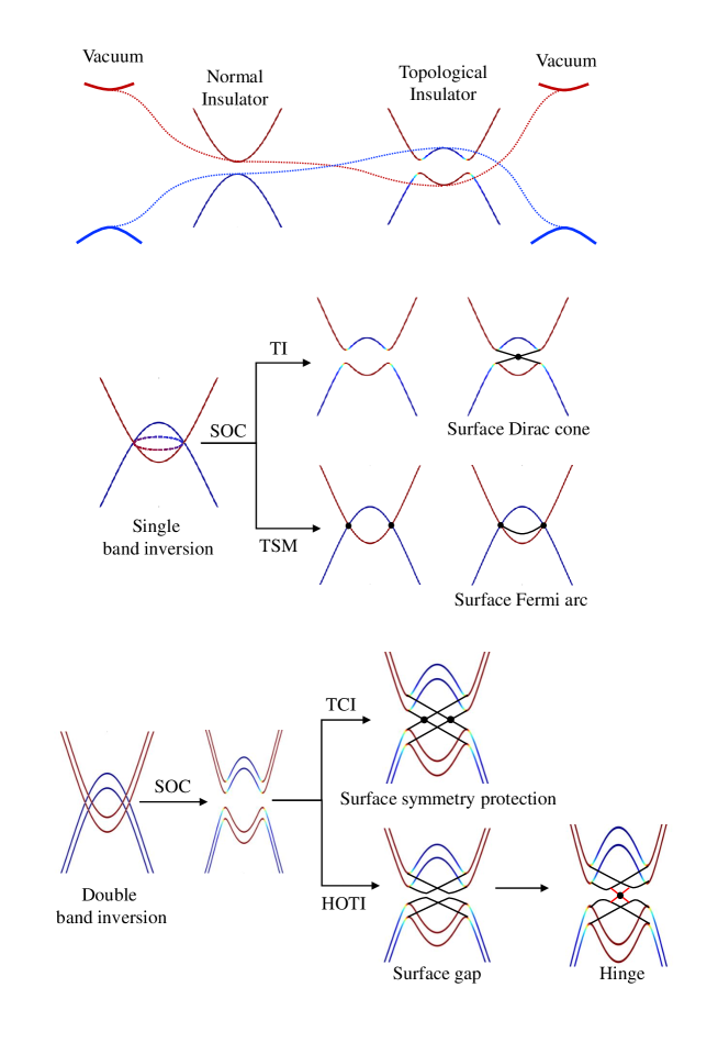
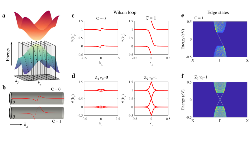
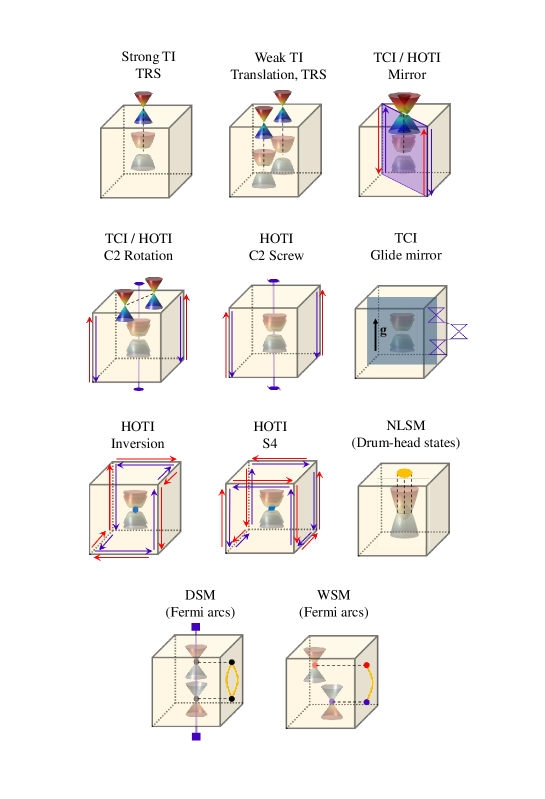
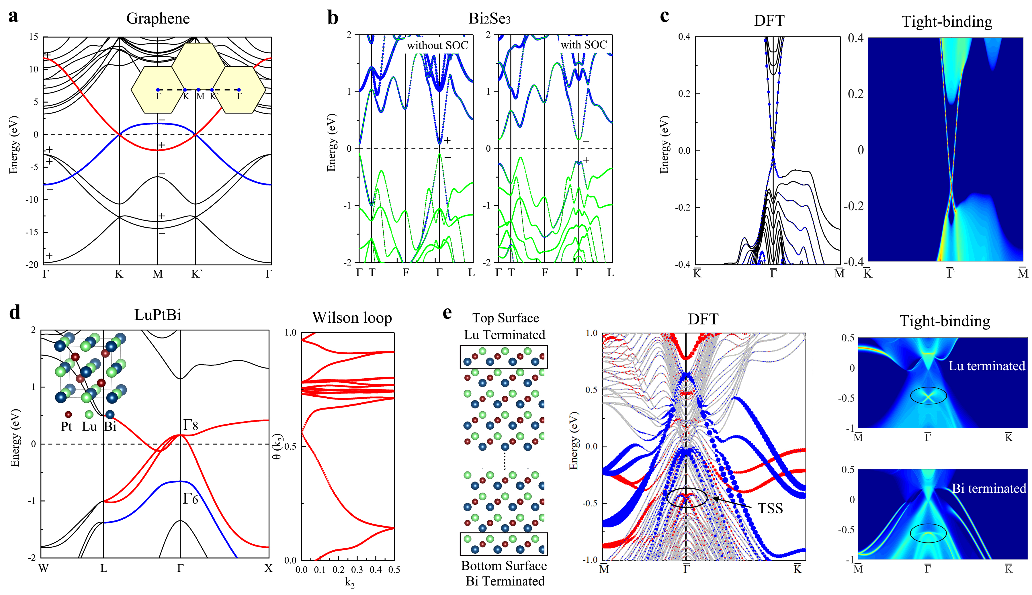
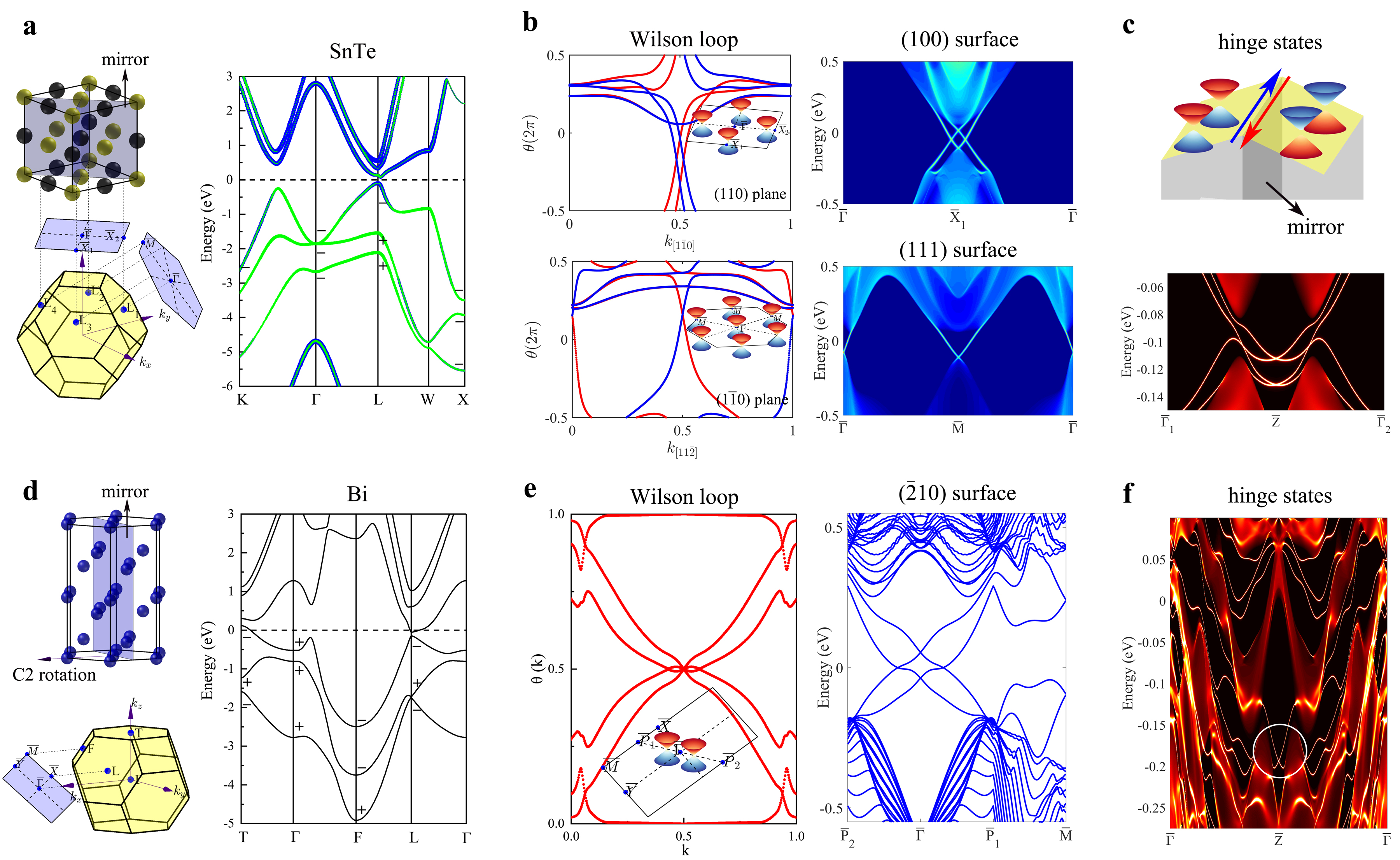
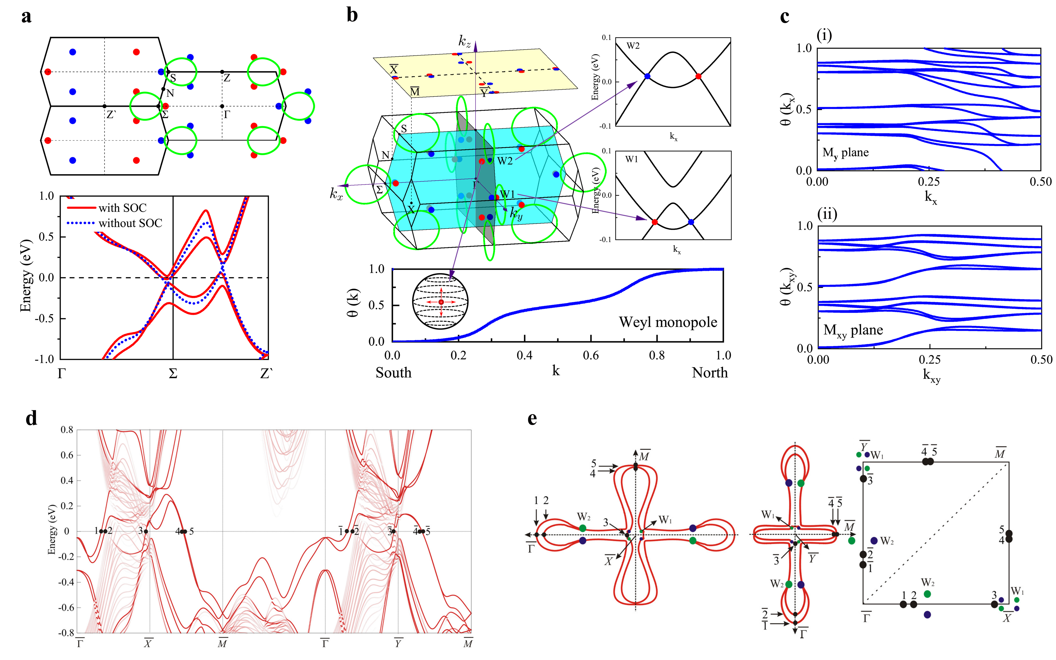
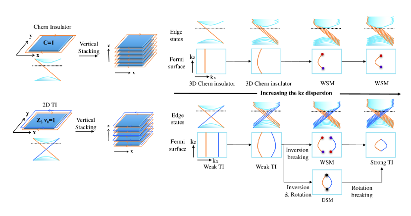
Key references:
Ref.6 proposed the parity criteria and used them to predict topological insulator materials.
Refs. 58, 59, 60 proposed the method of Wannier charge center evolution and Wilson loop to evaluate the topology.
Refs. 65, 66, 63, 64, 68 proposed the symmetry indicators to classify general topological states and materials.
Refs. 1, 3, 4 are well known examples for materials prediction.
Glossary terms:
Space group. A symmetry group that includes all crystal symmetries. There are 230 space groups in total for 3D crystals.
Irreducible representation. For a space group, a representation is a set of matrices, each of which responds to a symmetry operation. The relation of symmetry operations is equivalent to the calculation of matrices. The irreducible, block-diagonal form of the matrix representation is called irreducible representation.
Wyckoff positions. In a space group, Wyckoff positions denote the symmetry-allowed positions, including sites and multiplicity, where atoms can be found.
Website summary:
First-principles calculations have been very successful in predicting topological quantum materials. This Technical Review covers topological band theory and provides a guide to the study of topological materials with the first-principles methods.