Supplementary Materials:
Exploiting Aharonov-Bohm oscillations to probe Klein tunneling in tunable pn-junctions in graphene
1 Supplementary details on experiment
Sample fabrication
The heterostructure was made from CVD grown graphene and mechanically exfoliated hBN by van der Waals assembly and was placed on a highly doped Si substrate with a nm dry thermally grown SiO2 top layer. The structure was patterned and contacted using standard electron beam lithography, reactive ion etching with a SF6/Ar plasma and electron beam evaporation. An Al hard mask was used for etching. Contacts were made of Cr/Au ( nm/ nm). The structured and contacted device was covered with an additional hBN flake as gate dielectric and subsequently a partial top gate was built with similar processes as for the contacts, but with Cr/Au ( nm/ nm). Before measurements the device was heat annealed in Ar/H2 atmosphere at C for several hours.
Device characterization
Fig. S1 displays optical and scanning force microscopy (SFM) images of different stages in the device fabrication. The patterned and contacted hBN/graphene/hBN heterostructure is shown in Fig. S1(a). From this SFM image the dimensions of the ring were extracted ( nm, nm). Fig. S1(b) depicts the device after the transfer of the top gate hBN flake and top gate metallization. The top gate hBN flake adapted to the structure only to some extent and is partially suspended between metal contacts and etched heterostructure. The top gate followed the uneven surface, but the metal thickness was chosen sufficiently large to overcome the appearing height differences (top-gate metal Cr 5 nm/Au 145 nm ). At the top of the metal finger a spike appears, most likely an artifact of the lift-off process in the frame of top-gate metallization, but it had no effect on the top-gate functionality. An optical image of the final device is displayed in Fig. S1(c). All measurements were performed in wet dilution refrigerator with perpendicular magnetic field and at a base temperature of mK, unless stated otherwise. We used low-frequency AC lock-in techniques for simultaneous two and four-terminal measurements with a constant AC bias of V at Hz. Bias dependency is investigated by different bias voltages , where a constant AC bias V is overlayed with a variable DC bias .
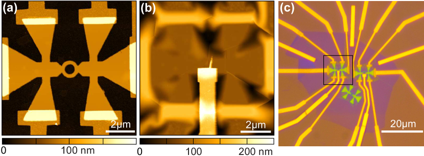
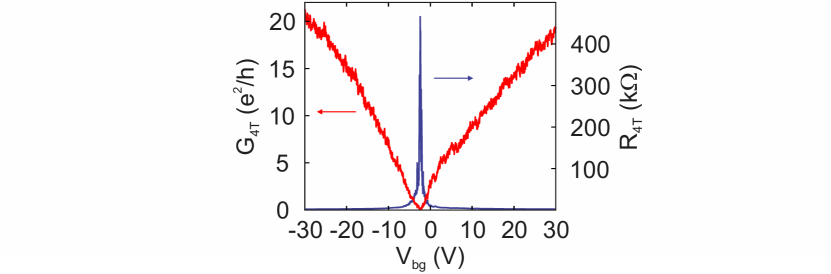
Fig. S2 shows the four-terminal conductance and resistance as function of back-gate voltage with a fixed relationship to top-gate voltage . The position of the charge neutrality point (CNP), V, and the slope are extracted by adjusting both parameters until the most linear and the sharpest peak of are found. Thus, the contributions from the two ring arms are aligned at best and only a single Dirac peak is visible in the gate characteristics. The slope is in good agreement with the distance ratio between the back-gate to the graphene ( nm) and the top-gate to the graphene ( nm). From the color plot of as function of and (see main text Fig. 1e) we extract a lever arm ratio of , which is in good accordance with the determined slope. With this relationship nearly equal charge carrier densities are achieved in both ring arms.
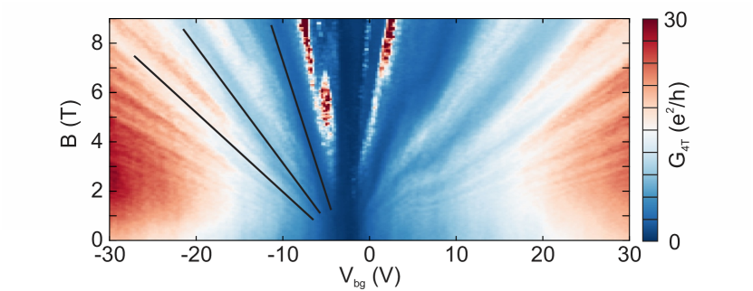
The same relationship of and is used to study the magneto-conductance of the device by quantum Hall measurements. We observe a graphene-typical Landau fan with integer Hall plateaus and an absent zero Landau level. At small, positive a bending of the Landau levels occurs, which coincides with a non-linearity in the gate characteristics (compare Fig. S2). This effect could arise from an inhomogeneous doping profile or localized state at the edge of the etched structure in combination with the complex electrostatic tuning of the device, but it is not fully understood. Following Ref. [Ki2012] we extract a back-gate lever arm cm-2V-1 over an average of filling factors and , which is in good agreement with a parallel plate capacitor model ( cm-2V-1, ).
.
Background subtraction and Fourier transform
Data post-processing is crucial to separate AB oscillations from other transport effects in mesoscopic systems, e.g. weak localization, universal conductance fluctuations (UCFs) and size effects. The magneto-conductance background beside UCFs changes rather slowly compared with the periodicity of the AB oscillations. Therefore these effects are easily filtered out by averaging.
The periodicity of AB oscillations is given by sample geometry ) with , where is the mode number. With our ring geometry nm and nm we calculate for the fundamental mode mT, mT and mT and the first harmonic mT, mT and mT. All other higher harmonics are calculated in a similar manner. This periodicity in magnetic field translates into an expected frequency range of T for , T for and T for in the Fourier spectrum. The periodicity of UCFs in a quasi-diffusive system can be estimated by [Huefner2010], where is the width of the ring and the phase-coherence length. Taking m (see main text and below) this estimate gives mT or a frequency of T-1, respectively. This frequency is clearly distinguishable from the expected AB oscillations and can be separated with an adequate filter method.
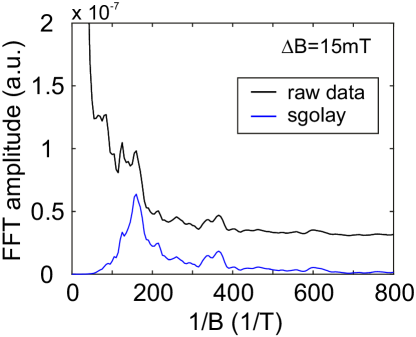
The magneto-conductance background is determined by filtering the four-terminal conductance over the span . The background subtracted conductance is calculated by subtracting the filtered data from the raw data and is used for further analysis of the AB oscillations. We choose a Savitzky-Golay filter [Savitzky1964Jul] with a 5th order polynomial and a span of approximately three periods of oscillations ( mT) for the extraction of the magneto-conductance background . This method provides higher filter dynamic and steeper filter edge compared to a moving average without distorting the signal tendency. In Fig. S4 we compare the Fourier transform of the raw data with the Fourier transform of the background subtracted conductance determined by the Savitky-Golay filter. Importantly, even in the raw data the frequency components of the AB oscillations and the first harmonic are recognizable, but overlapped with an exponentially decaying frequency background. The Fourier transform of the processed signal reproduces the very same features of AB oscillations as shown in the raw data and in addition removes the frequency background.
.
.
Additional data on Aharonov-Bohm oscillations
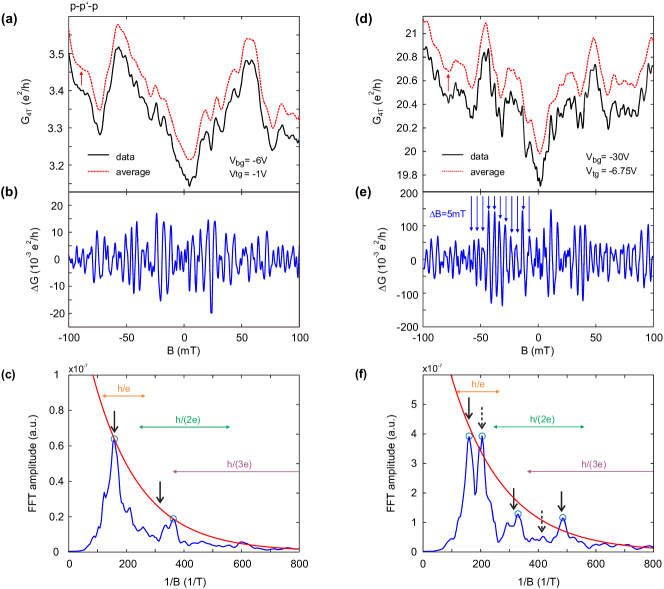
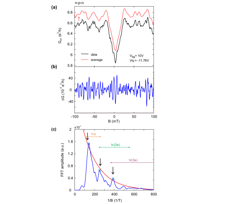
In the low magnetic field regime, we observe AB oscillations at all gate voltage settings independent of being in an unipolar or bipolar doping regime. In Figs. S5 and S6 we present additional data sets for the observation of AB conductance oscillations. Similar to Fig. 2 in the main text, the raw data of the four-terminal conductance , the background subtracted conductance and the Fourier transform of are displayed for two different gate configurations. Close to the CNP in the p-p’-p regime (see Fig. S5(a-c)) we find AB oscillations of the fundamental mode and the first harmonic and extract a m. For high charge carrier density in the p-p’-p regime (Fig. S5(d-f)) we observe an Fourier spectrum with higher harmonics up to and extract a m. In general we notice that for higher back-gate voltages and for similar charge carrier densities (and types) in both ring arms the higher harmonics are best visible in the Fourier spectra. With a homogeneous carrier density inside the ring, no pn-junctions or interface are formed, where backscattering could occur. Also, with increasing the mean free path increases making scattering more unlikely. Therefore, this regime is ideal for the observation of AB oscillations and their higher harmonics. Fig. S6 shows very similar data as shown in Fig. 2 of the main manuscript and in Fig. S5 but in the n-p-n regime.
Temperature and bias dependent measurements
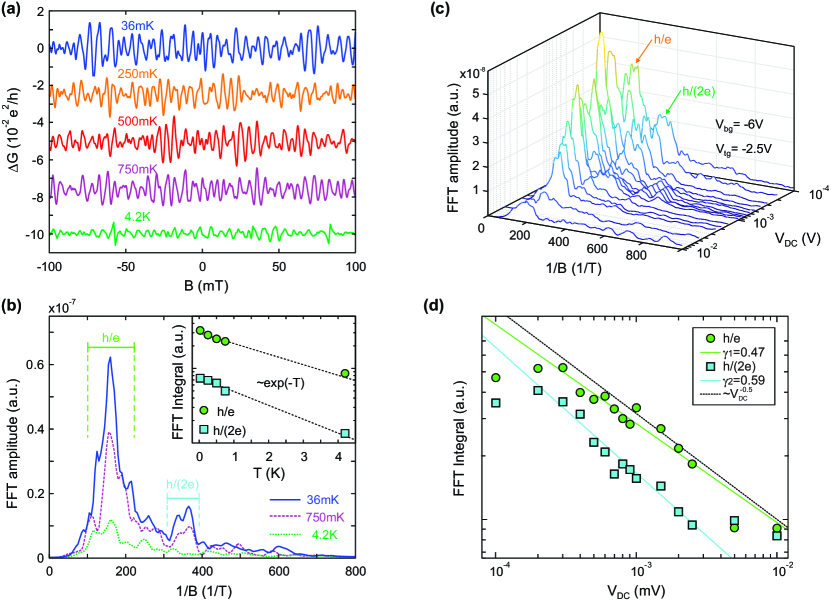
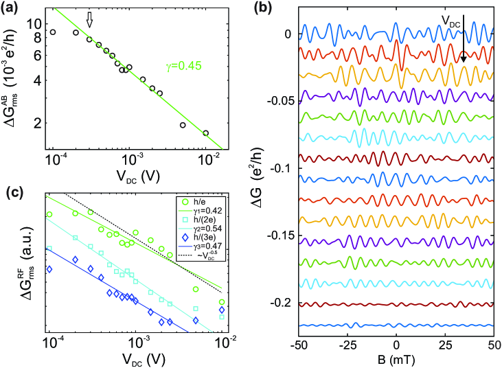
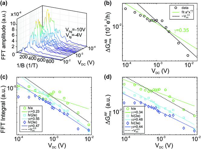
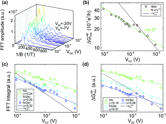
Fig. S7(a) shows AB oscillations measured at different temperatures . The amplitude decreases with temperature, while the periodicity is preserved. The Fourier transform of this data is displayed in Fig. S7(b), where the component is visible up to mK and the component is present even at K. Besides the decrease of amplitude slightly-different peak structures are observed with changing temperature. For a quantitative comparison, we calculate the integral of the and peaks over ranges as indicated in Fig. S7(b) (see vertical dashed lines). The data is well described by an exponential decay (see insert of Fig. S7(b)). Decoherence of AB oscillations is studied further by DC bias voltage dependent measurements, presented in a waterfall plot of the Fourier transform of as a function of inverse magnetic field (), as shown in Fig. S7(c). The amplitudes of the and the mode decrease with increasing and are nearly vanished at mV and mV, respectively. This decrease is quantified in Fig. S7(d), where the integral of the FFT amplitude over the two regimes (see vertical dashed lines in Fig. S7(b)) is plotted as function of in a double logarithmic plot exhibiting a dependency. Please note that a very similar behaviour is also found when plotting directly as function of (see Fig. S10(a)). The corresponding data of versus -field for different are shown in Fig. S10(b).
Two mechanisms lead to phase decoherence at sufficient low temperatures: (i) Energy smearing of the quantum state eigenenergies and (ii) changes of the phase coherence length affecting the amplitude of AB oscillations:
| (1) |
where is the Thouless energy given by with the typical traversal time [Ren2013, Russo2008]. Finite temperature or applied DC bias voltage lead to an energy smearing of . If is larger than , uncorrelated energy levels contribute to transport averaging out electron interference effects proportionally to [Ren2013]. We estimate , assuming a diffusive [Russo2008] or ballistic system [Mur2008] with , of eV (diffusive) and eV (ballistic), respectively. From the bias dependent measurements we extract a critical bias voltage of V (see arrow in Fig. S10(a)). This value is between the two cases and we conclude that our device is a quasi-ballistic mesoscopic system, where the electron mean free path is between the sample dimensions ().
At low temperatures is mainly influenced by electron-electron interaction [Hansen2001] and in two dimensional systems the phase-breaking time is found to be [Altshuler1982]. Below we observe an exponential decay , which again points towards a ballistic () rather than a diffusive () system similar to experiments in GaAs/(Al,Ga)As heterostructures [Hansen2001]. Please note that a critical bias voltage of V corresponds to a critical temperature of K and that most of our measurements have been performed well below .
More details and additional data
For the analysis of the amplitude of the AB oscillations as function of DC bias voltage we used in total three different methods. First we simply take the RMS value of the background subtracted conductance given by , as it was used by many other groups before [Russo2008, Ren2013]. The second approach (FFT integral) is based on the integration of the Fourier spectrum of with respect to different frequency ranges of the various AB modes. Thus, the amplitudes of the , and mode are extracted individually and only contributions in the specific frequency ranges are taken into account. For the third method (reverse Fourier (RF) RMS) only the frequency components of the , and mode are taken from the Fourier transform of and individually re-transformed by reverse Fourier transformation. From the reverse Fourier transformed conductance the RMS value, , is determined as a measure of the amplitude of the different modes . This procedure combines the simplicity of RMS value with frequency selectivity of the Fourier transformation. Although the three methods are based on quite different means, the obtained results are found to be very similar. The independence of the observed behavior from the specific method proves the functionality of the (simple) amplitude analysis. Since the results are very similar, we choose the FFT integral of the AB mode ranges in the Fourier spectrum as used measure for further AB amplitude and decoherence investigations in temperature and bias dependent measurements. Nevertheless, we show all three different methods for measuring decoherence as function of DC bias voltage and additional data for higher charge carrier densities in Figs. S8 to S10. While the FFT integral analysis is shown in Fig. S9(d), Fig. S10(a) depicts and Fig. S10(c) as function of DC bias voltage at V and V. Each data set is fitted with a power law , where the first, second and third mode of AB oscillations. For only a single fit is made (see Fig. S10(a)). These results validate our findings above and also show a critical DC bias voltage of around V with a decay of the AB amplitude afterwards. More data of very similar analysis are shown in Figs. S9 and S10. Figs. S9(a) and S10(b) show the waterfall plots of Fourier transforms as function of DC bias voltage and the three amplitude analyses at V and V and at V and V, respectively. Here, we observe a shift of to higher bias voltages as the charge carrier density increases. Also a decrease of the AB amplitude occurs below , but much weaker than . The shift of could arise from an enhanced mean free path with increasing . Hence, the diffusive constant increases and therefore also and . The decoherence mechanism below is not fully understood. Without energy smearing of quantum state eigenenergy, changes in can influence the AB amplitude. As is limited mainly by electron-electron interaction at low temperatures [Hansen2001], it may be affected by DC bias voltage, but further investigation is required for a better understanding.
Additional data on the interplay of AB oscillations and Klein tunneling
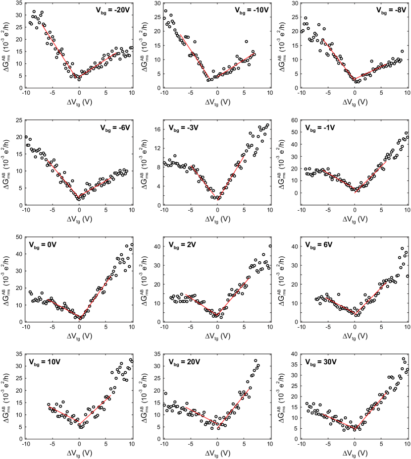
In Fig. S11 we present all other data sets of AB amplitude versus for different in order to investigate Klein tunneling by AB oscillations. Each panel displays the AB amplitude by the RMS value of , , as function of for a specific . Together with the data shown in the main text ranges from V to V. The linear fits for the extraction of the amplitude asymmetry are included in the amplitude profiles . As described in main text we observe an asymmetry around the top-gate CNP. In vicinity of the back-gate CNP of the device the profiles are almost symmetric (see e.g. V). The asymmetry switches at the back-gate CNP and increases towards high back-gate voltages.
2 Supplementary details on theory
Theoretical model for the oscillatory conductance
In this theoretical analysis, we model our device as a scattering region between two leads. We assume that these leads are identical and host a number of states, denoted by , which depends on the Fermi energy. As our experiments are performed at very low temperature, we assume that in our theoretical model. Taking into account both spin and valley degeneracy, we can then express the conductance of our device as [Buettiker1985]
| (2) |
which is valid in the linear approximation in the bias voltage . The factor expresses the transmission probability from channel in the incoming lead to channel in the outgoing lead. Throughout this section, we consider positive Fermi energies , i.e. we consider incoming electrons. Because of electron-hole symmetry, the corresponding results for holes can easily be derived.
Our device consists of a ring, with a lower and and upper arm. In the lower arm, a top gate voltage induces a potential energy , with maximum . A complete calculation of the transmission through the device takes into account direct transmission through the upper and lower arms of the ring, as well as paths that encircle the entire ring, either once or multiple times. For a ring with a single channel, all these contributions were added in Ref. [Gefen1984], where the authors obtained an analytical result for the transmission. Their result is valid in the limit where the phase coherence length is much larger than the size of the ring. In our experiment, is however on the order of , as was previously extracted from the data in Fig. 2, Figs. S5 and S6. Due to loss of coherence, the contribution to the Aharonov-Bohm oscillations of paths that encircle the ring times is suppressed by a factor , which is small in our case. These paths, which show up as higher harmonics in the Fourier spectrum, therefore play a much smaller role in the transmission. We thus believe that we can obtain a good estimate for the total transmission by taking only direct transmission through the upper and lower ring arms into account.
We can label the modes in the incoming lead by their transversal momentum . Electrons in these modes are partially transmitted to the various modes in the upper and lower ring arms, and partially reflected. The electrons that are transmitted into the ring arms are subsequently partially transmitted to the modes in the outgoing lead. In principle, all incoming modes can couple to all outgoing modes through all different modes in the lead, as discussed in more detail in Ref. [Buettiker1985]. In this calculation, we will however assume that scattering between different modes only plays a minor role, and therefore neglect it. This means that an electron with transversal momentum is transmitted, with a certain probability, to a mode with transversal momentum in the ring arm, and subsequently transmitted to a mode with transversal momentum in the outgoing lead, again with a certain probability. The idea behind this assumption is that is conserved across the np- and nn′-junctions that arise in the lower ring arm, because we can model these junctions by a one-dimensional potential , as we discuss later in somewhat more detail. This description seems reasonable because the junction width is much smaller than the ring circumference (). Admittedly, this assumption is fairly crude, and means that we certainly miss different contributions. However, we believe that the description allows us to capture the main mechanism, while at the same time keeping the model analytically tractable.
The first consequence of this assumption is that we only consider the diagonal elements in equation (2), i.e.,
| (3) |
Note that we add the contributions of the various modes incoherently in this equation. Furthermore, the assumption also implies that we can write as
| (4) | ||||
| (5) |
where represents the tunneling through the upper (lower) ring arm as a function of . We can write the transmission coefficients through the arms as
| (6) | ||||
| (7) |
where we have adopted a semiclassical picture in order to write the phase as a sum of the (geometrical) Aharonov-Bohm phase and the dynamical phase. Adding all different channels, we obtain
| (8) |
As the magnetic field is weak, and mainly serves as a probe, we can assume that the absolute values of the tunneling amplitudes do not depend on it. This approximation implies that the first two terms in the above equation are independent of the magnetic field and do not contribute to the Aharonov-Bohm oscillations. The last term describes interference between electrons going through the different ring arms and thus describes the Aharonov-Bohm oscillations. Note that one could, in principle, include the magnetic field in the tunneling amplitudes using the results from Ref. [Shytov2008].
Using equation (7), we can therefore write the oscillatory part of the conductance as (8) as
| (9) |
To a first approximation, the Aharonov-Bohm phase is independent of , as the majority of the magnetic flux goes through the ring opening, and a much smaller part through the arms of the ring. This means that we can take the Aharonov-Bohm phase out of the summation and use Stokes’ theorem to obtain
| (10) |
In order to determine the root mean square of the Aharonov-Bohm oscillations,
| (11) |
where denotes the averaging over the magnetic field, we use the identity
| (12) |
Since in our case contains an oscillating function, only the third term remains after the averaging. We thus obtain
| (13) |
We now assume that the dynamical phase only weakly depends on . In the lowest order approximation, we can then neglect this dependence, and take the phase factor outside of the summation. Due to the absolute value, it subsequently disappears from the result. In the npn-regime this assumption can be partially justified, since the transmission is largest around normal incidence (zero transversal momentum), and decays rapidly with the angle of incidence, depending on the effective width , as we discuss in the following section. We also remark that this assumption leads to an overestimation of the transmission amplitudes, as the triangle inequality gives
| (14) |
Note that, according to our assumption, a change in the gate potential leads to a global phase shift of the Aharonov-Bohm oscillations, once the background has been subtracted. Previous experiments [Ford1989b] on gated Aharonov-Bohm rings in GaAs/AlGaAs heterostructures show that this system actually exhibits much richer behavior. In these experiments, the phase seemed to be “pinned” near , as it did not change substantially between different top gate voltages. This pinning may have been a consequence of the Onsager relations, see also Refs. [Buettiker1985, Yacoby1996]. In the experiment [Ford1989b], amplitude modulations as a function of the top gate voltage , which controls the potential , were also observed. However, contrary to our experimental observations, these modulations were periodic. This leads us to believe that, in our experiment, the change in the root mean square of the Aharonov-Bohm oscillations between different top gate voltages is mainly caused by the modification of the transmission coefficient, and only to a lesser extent by the modification of the interference, in agreement with our model. Our approximation for therefore reads
| (15) |
where we have introduced the average tunneling amplitude , which equals the product of the transmission probabilities through the upper and lower ring arms, averaged over all modes in the lead. We note that its value lies between 0 and 1.
Our next step is to obtain a formula for the average tunneling amplitude . As both the leads and the ring arms are quite wide, we invoke the continuum approximation to perform this computation. We thus assume that all parts of the system host a continuum of states. Within this limit, the quantized momentum becomes the continuous transversal momentum . As we already discussed before, we model the np- and nn′-junctions, which arise in the lower ring arm, by a one-dimensional potential , since the junction width is much smaller than the ring circumference (). This implies that is conserved across the junction interface. When we take the continuum limit, we therefore convert the sum over the various modes in the definition of into an integral over and incorporate the distribution of the transversal momenta through a continuous distribution function . To ensure that the transmission lies between zero and one, we normalize by the integral of this distribution. This leads to
| (16) |
Studies of billiard models [Beenakker89, Milovanovic13, Milovanovic15, Reijnders17, Reijnders17b] show that the initial distribution can usually be well approximated by a uniform distribution. Since the upper arm of the device is not gated, we set , which means that we neglect scattering at the inlet of the ring.
Since we have invoked the continuum approximation, the charge carriers obey the classical dispersion relation [Reijnders13, Tudorovskiy12] , which shows that a classically forbidden region appears for . When the maximum of the potential satisfies , we have two nn′-junctions in the lower ring arm. However, by virtue of the dispersion relation, we only find classically allowed electron states between these two junctions for incoming states that have a transversal momentum which satisfies . Thus, more states become available inside the lower ring arm when we decrease the potential , as the inequality is satisfied for more values of , which, by virtue of equation (16), leads to an increase in and therefore to an increase in the amplitude (15) of the Aharonov-Bohm oscillations. When there are classically allowed electron states in the lower ring arm, we set the tunneling amplitude to unity. When these states are absent, we set the tunneling amplitude to zero. Although, in the latter case, charge carriers can theoretically tunnel through the region between the two junctions, the corresponding amplitude is exponentially small [Reijnders13] and can be neglected. Likewise, we neglect the exponentially small reflection for the nn′-junction [Reijnders13].
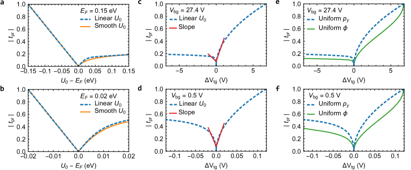
Similar considerations hold for the case , which leads to an np- and a pn-junction in the lower ring arm. There are classically allowed hole states in the lower ring arm when the transversal momentum of the incoming electron state satisfies . This inequality is satisfied for more values of when increases, similar to the previous case. However, this time the tunneling amplitude is smaller than one, as the electrons have to tunnel through a classically forbidden region [Reijnders13, Tudorovskiy12]. By virtue of equation (16), this implies that the slope of is smaller for than for . These considerations qualitatively explain the shape of the curves in Figs. 3a-d of the main text and Fig. S11.
Derivation of the tunneling amplitude
In order to obtain a more quantitative comparison between theory and experiment, we compute the average tunneling amplitude explicitly. We focus on the case of an npn-junction, noting that similar considerations hold for the nn′n-junction.
We first note that we can neglect multiple reflections within the junction. Since both the mean free path and the phase coherence length of the charge carriers are smaller than or on the order of , the contribution of multiple reflections to the transmission amplitude is suppressed. Within a semiclassical framework [Reijnders13], we can then write down the absolute value of the tunneling amplitude through the lower ring arm as
| (17) |
Since we consider the absolute value of the tunneling amplitude, we do not have to compute its phase, which contains the classical action of the particle along its trajectory in the lower ring arm.
Previously, we assumed that scattering between different modes only plays a minor role, and therefore neglected it. In the continuum approximation, this enables the factorization (17). We nevertheless note that this is a fairly crude approximation, since the magnetic length is about nm for a magnetic field of mT. Within a continuum semiclassical picture, the transversal momentum may therefore change somewhat within the lower (and similarly in the upper) ring arm. We nevertheless resort to this approximation, as computing the variation of requires very large additional efforts. Furthermore, we neglect edge scattering, which is strongly suppressed for sliding electrons with zigzag edges [Dugaev13]. Note that generic edges behave fairly similar to zigzag edges [Akhmerov08] and in particular do not lead to valley mixing.
We can obtain an analytic expression for by considering a linear potential , i.e., for and is constant outside of this regime. The tunneling amplitude is then given by [Cheianov2006, Tudorovskiy12]
| (18) |
where we have introduced the dimensionless effective junction width . The same expression holds for when we consider a linear pn-junction. Using equations (16), (17) and (18) and assuming that (), we then obtain
| (19) |
Note that we integrate from to , since the tunneling amplitude is zero for values of outside of this regime because we are no longer dealing with an npn-junction. Using the definition of the so-called error function, , we can rewrite this expression as
| (20) |
Note that this expression is only valid for , as, within our approximation, no new states in the lower ring arm become available beyond .
Expression (20) shows that increases by two mechanisms when we increase the potential . First of all, the error function increases. From a physical point of view, this corresponds to new modes that become available within the lower ring arm. Second, the prefactor increases, which corresponds to increased transmission through the available modes. We can now identify two regimes in our model. For small , we can expand the error function to first order in its argument to obtain . Hence, the combination of both mechanisms leads to a linear increase of the average tunneling amplitude . At large values of , the error function has saturated and the second mechanism dominates: the tunneling amplitude increases like a square root.
Since , we may estimate that the transition between these two regimes lies close to
| (21) |
Crucially, this factor strongly depends on the effective junction width . At small , we mainly observe the first regime where increases linearly. This leads to a symmetric situation where the npn- and nn′n-junctions display similar behavior, see Fig. S12(b). On the other hand, for large we mainly observe the second regime, which leads to a much slower increase in , see Fig. S12(a).
In order to obtain results for more realistic potentials , we can use the semiclassical approximation for the tunneling amplitude. Within this scheme, is given by [Reijnders13, Tudorovskiy12, Shytov2008, Cheianov2006]
| (22) |
where is the classical action in the classically forbidden region and are the classical turning points, which satisfy . Note that this approximation correctly reproduces the exact result (18) for a linear potential. As shown in Figs. S12(a) and S12(b), the smooth potential increase
| (23) |
which has the same slope at as the linear potential, leads to qualitatively similar results for the averaged tunneling amplitude .
Derivation of the normalized difference of the slopes
To compare our theoretical predictions with the experimental observations, we extract the slopes of . Within our theoretical model, this slope is directly proportional to the slope of , see equation (15), where the proportionality depends on the Fermi energy . However, our theoretical model predicts that large increases in the transmission only occur for . Figs. S12(c) and S12(d) show that this leads to a fitting regime that strongly depends on , i.e. on , in contrast to the experimental observations shown in Fig. S11. This difference is due to the many simplifications that we have made throughout the model. In particular, the upper and lower ring arms contain less modes than the leads, which implies that states can also be filled outside of the regime , leading to an increase in the amplitude of the Aharonov-Bohm oscillations. However, we may assume that our simplifications affect the transmission on both sides of the charge neutrality point in a similar way, which means that the prediction for their ratio is much more accurate. Rather than comparing the individual slopes with the experimental data, we therefore focus on the normalized difference of the slopes.
Our next step is to carefully think about an appropriate interval that we can use to determine the slopes, as we cannot use the experimental interval. As we discussed in the previous section, our model exhibits two regimes. The transition point between these two regimes is roughly given by equation (21) and crucially depends on . Since large increases in the transmission occur for between and , we parametrize our fitting interval as for the nn′n regime and for the npn regime. If we choose too small, we overestimate the influence of the first regime. On the other hand, if we choose it too large, the influence of the second regime is overestimated. We therefore believe that should ideally lie somewhere around . After choosing , we convert these energy intervals into intervals for the top gate voltage .
We can obtain an analytic result for the normalized difference of the slopes by approximating the slopes by the difference quotient, that is, by setting
| (24) |
Equation (20) shows that the transmission vanishes at the charge neutrality point, in other words that . Since we also have , we arrive at
| (25) |
Combining equation (20) with the observations that and that , we finally obtain
| (26) |
Note that all prefactors have canceled in this equation, and the normalized difference of the slopes only depends on the transmission coefficients. Setting in formula (26), we arrive at equation (3) of the main text. In Fig. S13(a), we plot our result (26) for three different values of . Importantly, all three curves predict a similar dependence of on . However, the attained values depend on the value of . When , we attach greater importance to the first one of the regimes discussed in the previous subsection, leading to relatively small values of . On the other hand, we attach greater importance to the second regime when , leading to much larger values of . From a theoretical point of view, setting seems to be a good compromise.
We can compare our equation (26) with the result obtained by determining the slopes of the transmission (20). When we use the fitting intervals discussed above with , we observe that the result nicely coincides with our equation (26) with , as shown in Fig. S13. We performed the curve fitting for the graphs of versus , as shown in Figs. S12(c) and S12(d), in order to be consistent with the procedure for the experimental data. However, performing the fitting for the graphs of versus does not substantially change the result.
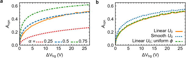
In Fig. S13(b), we compare the normalized difference of the slopes extracted for a linear potential and for the smooth potential (23). We observe that a smooth potential leads to exactly the same shape of the curve, although slightly higher values of are attained. We also show what happens when we use a uniform angular distribution for in equation (16), instead of a distribution that is uniform in the transversal momentum . Although the transmission curves are significantly altered, as shown in Figs. S12(e) and S12(f), the normalized difference of the slopes remains the same. Hence, we conclude that the distribution function has only a minor influence on (and ).
References and Notes
- [1]