Adaptive Background Compensation of FI-DACs with Application to Coherent Optical Transceivers
Abstract
This work proposes a novel adaptive background compensation scheme for frequency interleaved digital-to-analog converters (FI-DACs). The technique is applicable to high speed digital transceivers such as those used in coherent optical communications. Although compensation of FI-DACs has been discussed before in the technical literature, adaptive background techniques have not yet been reported. The importance of the latter lies in their capability to automatically compensate errors caused by process, voltage, and temperature variations in the technology (e.g., CMOS, SiGe, etc.) implementations of the data converters, and therefore ensure high manufacturing yield. The key ingredients of the proposed technique are a multiple-input multiple-output (MIMO) equalizer and the backpropagation algorithm used to adapt the coefficients of the aforementioned equalizer. Simulations show that the impairments of the analog signal path are accurately compensated and their effect is essentially eliminated, resulting in a high performance transmitter system.
Index Terms:
Frequency interleaving DAC, high-speed optical transmitter, background calibration, error backpropagation.I Introduction
Intensity modulation and direct detection in long haul and metro optical fiber links have been displaced by coherent transmission techniques [1, 2]. Next generation coherent transceivers will operate at symbol rates of 128-150 GBd and beyond [3]. The main challenge in the design of transceivers for high-speed optical communications is achieving the large bandwidth (BW) and sampling rate required by the analog-to-digital and the digital-to-analog converters (ADC and DAC). One of the solutions proposed in recent literature is the use of frequency interleaving (FI) techniques [4, 5].
This paper focuses on FI-DACs in the context of applications to transceivers for digital communications, particularly high baud rate coherent optical transceivers. Although laboratory experiments with high baud rate optical transmission based on FI-DAC have been described in the technical literature [6], significant obstacles remain before this technology can be applied in commercial products. One of the main challenges is how to automatically compensate the impairments of the analog signal path. As it shall be discussed later, because of process tolerances, layout limitations, etc., errors may exist which, if left uncompensated, would introduce large distortions and severely degrade the performance of the system. Several techniques have been presented to compensate analog errors in FI architectures. In previous work [7], the compensation requires startup calibration which is done using foreground techniques. In coherent optical systems, the latter would imply the interruption of the communication to compensate the imperfections, which is undesirable. The compensation needs to be accurately tailored to the impairments, which are process, voltage, and temperature dependent and (slowly) time variant. The only way to achieve this at low cost and in a way that lends itself to high volume manufacturing is to use adaptive background compensation techniques. However, no adaptive background compensation techniques for FI-DACs have been reported so far in the technical literature.
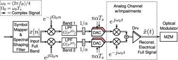
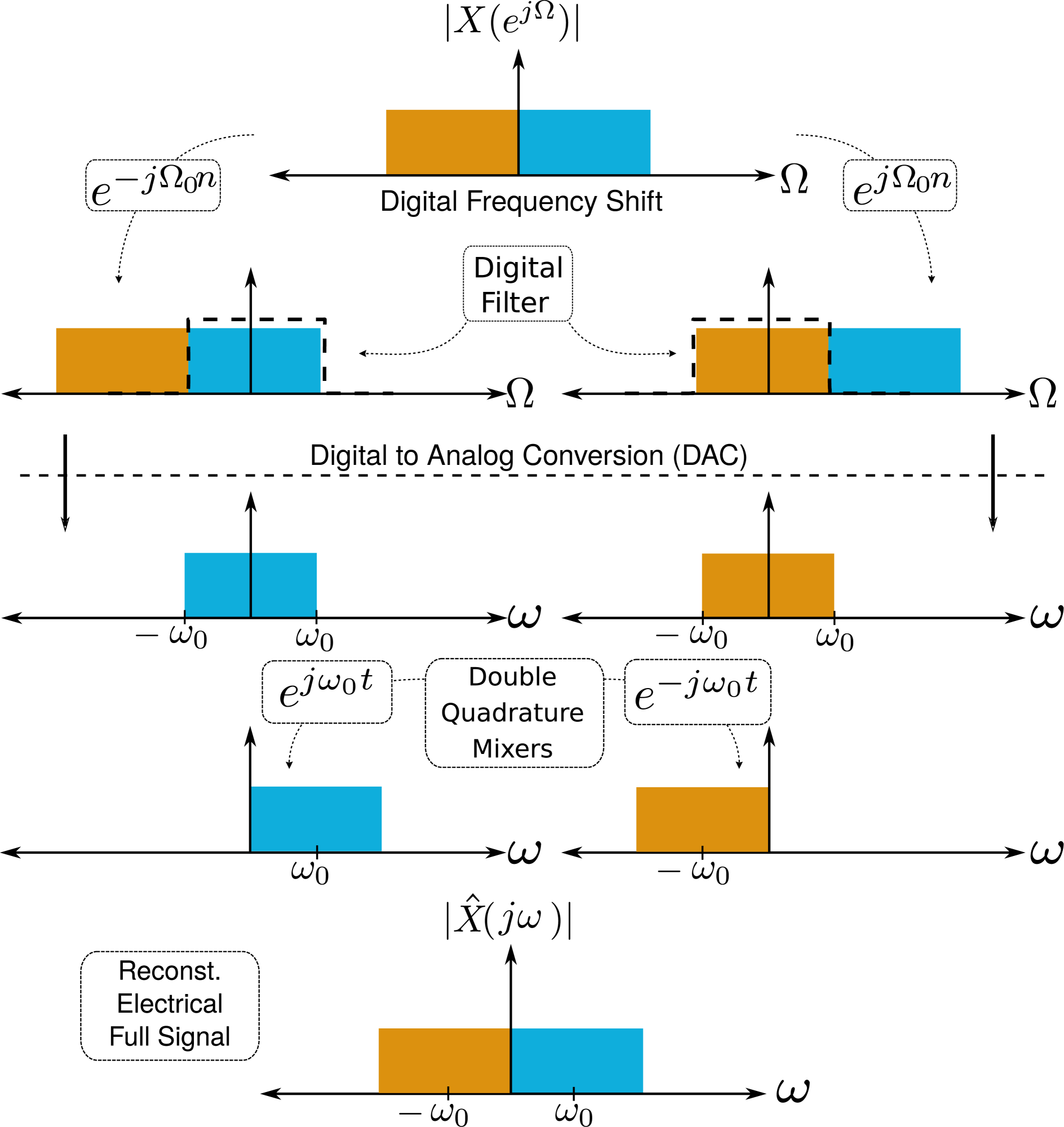
The FI-DAC architecture considered in this paper is shown in Fig. 1. It is discussed in the context of its application to a high baud rate transmitter for coherent optical communications. The scheme of Fig. 1 corresponds to one polarization in a dual-polarization (DP) coherent optical transceiver. The transmit path is partitioned into two or more bands by DSP techniques. Without loss of generality, in this paper we assume that it is decomposed into two bands. As shown in Fig. 2, each band is demodulated to baseband with two exponentials where with and being the DSP sampling rate. The demodulated baseband signals are first processed by lowpass filters (LPF) with frequency response , then they are downsampled by a factor , and synthesized by DACs of lower bandwidth and sampling rate than required by the full signal. After synthesis, analog double quadrature mixers reconstruct the full signal, which, after amplification by a modulator driver, is used to control the Mach-Zehnder Modulator (MZM)111As discussed in Section II, the analog path compensated by the scheme proposed here includes the impairments of the modulator driver and the interconnections among the FI-DAC, the driver, and the MZM. Said analog path may encompass components in different packages and printed circuit board (PCB) interconnects.. The reference clocks of the mixers and the DACs are assumed to be properly synchronized. To process even larger BW signals, this technique can be extended to more subbands, which would require more DACs with similar characteristics as those just described.
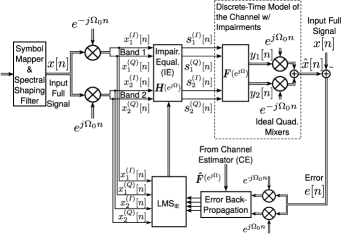
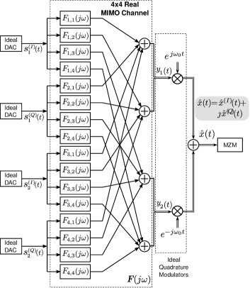
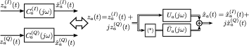
In this work we show that all analog impairments in a two-band FI-DAC can be modeled as a multiple-input multiple-output (MIMO) real filter defined by a transfer matrix , followed by ideal quadrature modulators (see Section II). Fig. 3 depicts a block diagram of the proposed compensation architecture and an equivalent discrete time model of the two-band FI-DAC based coherent optical transmitter. To compensate the effects of the impairments , we introduce a MIMO adaptive equalizer called hereafter Impairment Equalizer (IE) and defined by the transfer matrix , which includes the LPF responses . Let be the error between the reconstructed () and the original wideband () full signal. This error is measured at the input of the MZM (note that includes all the impairments of the analog path up to the input of the MZM). Then, the IE is adapted to minimize the mean squared error (i.e., ) by using the least mean square (LMS) algorithm. Towards this end, the digital backpropagation algorithm [8, 9] is proposed to perform background compensation of the channel impairments222Alternatively, the forward propagation algorithm [10] could be used. This option will be described in detail in a future paper.. This algorithm, in combination with the estimated channel response , provides the error samples required by the LMS algorithm to adapt the coefficients of the IE. Computer simulations demonstrate that the proposed IE architecture is able to compensate not only DACs and mixer impairments, but also the amplitude and phase distortions of the electrical paths (e.g., it acts as pre-emphasis and/or compensator of time skew between in-phase and quadrature (I&Q) components).
The rest of this paper is organized as follows. Section II introduces a model of the channel impairments in FI-DACs for a coherent optical transceiver. Section III describes the proposed adaptive background compensation technique. Section IV presents simulations and finally conclusions are drawn in Section V.
II Model of Analog Impairments in FI-DACs
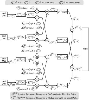
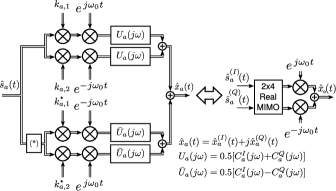
Analog impairments drastically affect the performance of any FI-DAC architecture, including the one presented here. The most important ones for a two-band FI-DAC based optical coherent transmitter are shown in Fig. 4 and include: (i) distortion, bandwidth limitation, and (in-band) time skew () caused by mismatches among electrical path responses between DACs and the quadrature mixers (denoted as with ); (ii) gain and phase errors (denoted, respectively, as and with ) of quadrature mixers employed for the reconstruction of the full analog signal; (iii) distortion, bandwidth limitations, and time skew () caused by mismatches among the electrical path responses going from the quadrature mixers to the optical modulator (denoted as with which include the modulator drivers and any other components in the signal path). The effect of the phase and gain errors in the quadrature modulators is to create spurious terms that cause interference in the adjacent band. As we shall show later, this interference as well as the other impairments can be compensated by the technique proposed in this paper.
Based on simple trigonometric identities and signal processing techniques, we show in the Appendix that the analog channel model with impairments for one polarization described in Fig. 4 can be reformulated as a MIMO real channel defined by a transfer matrix with elements , followed by ideal quadrature modulators (see Fig. 5). Based on this result, we can derive a simple discrete time model of the FI-DAC architecture for application in an optical coherent transmitter as depicted in Fig. 3. This formulation is important since it shows that all the impairments in FI-DACs can be digitally compensated by a MIMO compensator equalizer with transfer matrix . For example, for an ideal compensation, we get that where is the identity matrix and is the Fourier transform (FT) of the lowpass filter impulse response depicted in Fig. 1.
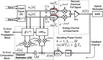
II-A Channel Estimator (CE) Block
As we shall discuss in the next section, the proposed compensation scheme is based on the evaluation of the error and the background estimation of the analog path response with impairments, . These operations are based on the samples of the output signal as depicted in Fig. 6. The feedback path includes buffers and track and holds (T&H) to support the bandwidth of the reconstructed full signal . However, since channel impairments change slowly over time, the estimation algorithm does not need to operate at full rate. Therefore, low power, low speed (i.e., with ), medium resolution ADCs with adjustable sampling phase can be used. The estimation of the analog channel response can be achieved by using the LMS algorithm (LMSCE) and the error between the DAC inputs (e.g., and ) and the samples of the reconstructed full signal as depicted in Fig. 6. Notice that CE block is also able to provide samples of the reconstructed signal at full rate for computation of the error . The response of the feedback path (i.e., T&H, ADC) could be initially estimated and removed from (the details are omitted due to space constraints).
III Adaptation of the Impairment Equalizer (IE): Error Backpropagation Algorithm
The samples of the reconstructed full signal for one polarization can be expressed as (see Figs. 3 and 5):
| (1) |
where and with components given by
| (2) |
where () denotes the FT (inverse FT) operator, is the real vector defined by while is the real vector with the digital samples at the DAC inputs.
Let with be the transfer function of the transfer matrix of the IE, . We also define the real impulse responses with . In this work we adopt the LMS algorithm to iteratively adapt the real coefficients of the set in order to minimize the mean squared error (MSE) between the input and the reconstructed full samples (LMSIE):
| (3) |
where denotes the number of iteration, , is the number of coefficients of the filters, is the adaptation step, and is the gradient of the MSE with respect to the real vector . The computation of the latter is not trivial since is not the error at the output of the IE (see Fig. 3).
To get the proper error samples to adapt the coefficients of the filters as expressed in eq. (3), we propose to use the backpropagation algorithm widely used in machine learning [8, 9]. Towards this end, we first generate the demodulated band errors and . These errors, in combination with eq. (2) and the estimated channel response , are used to get the backpropagated errors and (see [10, 8, 9] for a detailed description of the backpropagation technique). Finally, based on these backpropagated errors we can estimate the gradient as usual in the classical LMS algorithm.
Since channel impairments change slowly over time, the coefficient adaptation does not need to operate at full rate, and subsampling can be applied. The latter allows implementation complexity to be significantly reduced. Additional complexity reduction is enabled by: 1) strobing the algorithms once they have converged, and/or 2) implementing them in firmware in an embedded processor, typically available in coherent optical transceivers.
IV Simulations
We investigate the performance of the proposed background calibration technique in a two-band FI-DAC based DP coherent optical system by using computer simulations. We assume 16-QAM modulation with a symbol rate of GBd in a back-to-back optical channel. The oversampling factor used in the DSP blocks is . We consider 8-bit resolution DACs with sampling rate of 128 GS/s (i.e., in Fig. 1) and nominal BW of 32 GHz, which is half of what would be needed to process the input signal band in a non-interleaved architecture. The electrical analog path responses with in Fig. 4 are simulated with third-order Butterworth lowpass filters with nominal BW . Ideal feedback channel is assumed. The number of taps of the impairment equalizers is . The subsampling factor of the feedback ADC is . Other details of the DSP blocks are omitted due to space limitations (see [1] and references therein for details of typical DSP blocks).
We focus on the optical signal-to-noise ratio (OSNR) penalty333See [11] for a definition of OSNR penalty. at a bit-error-rate (BER) of , which is computed using an ideal software coherent receiver.
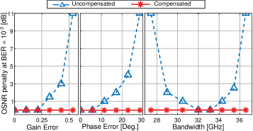
Fig. 7 shows the OSNR penalty as a function of the gain and phase errors of the quadrature mixers, and the bandwidth mismatches, respectively. Only one effect is exercised in each case. To stress the mismatch effects, the impairments are added only to the paths of signals and of each polarization (see Fig. 4). We present results with and without the proposed background compensation technique. The effectiveness of the IE architecture is verified in all cases. Notice that the proposed FI-DAC scheme performs very well in the presence of inaccuracies of the analog BW.
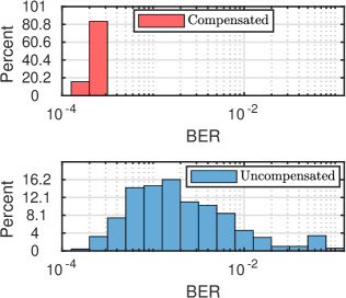
The robustness of the proposed compensation scheme was assessed by running Montecarlo simulations. A total of 500 channels with uniformely distributed random impairments such as gain errors (), phase errors (), and bandwidth mismatches (), were simulated. We set the OSNR to that required to achieve a BER in the absence of analog impairments. Fig.8 shows the histogram of the BER for the system with and without the MIMO equalizer. In all cases the excellent compensation of the impairments achieved by the proposed IE architecture is verified.
V Conclusions
An FI-DAC architecture with adaptive background compensation of the analog signal path errors for coherent optical transceivers has been presented. Simulations show the effectiveness of the proposed technique, which results in the elimination of the penalty caused by the DAC frequency response and the gain and phase errors in the mixers, as well as other impairments. Although the technique was presented in the context of a transmitter for coherent optical communications, it is more general and can be used in other applications.
Appendix
In this Appendix we derive the channel model of Fig. 5. With a proper design, it is possible to assume that the two cosine (and sine) signals used in each quadrature mixer have the same gain and phase444Although this assumption simplifies the math, it can be shown that it is not necessary for the applicability of the compensation scheme proposed in this paper., i.e., , , , and with . Note that and represent the gain and phase imbalance of the quadrature mixer for band , respectively. Then, based on the complex model proposed in [12], the modulator output of band denoted as (see Fig. 4), can be expressed as
| (4) |
where is the mixer input, and
| (5) |
with complex constants given by
| (6) | ||||
| (7) | ||||
| (8) | ||||
| (9) |
In the absence of gain and phase errors, notice that and . Fig. 9 shows the equivalent complex-valued model of the quadrature mixer with impairments.

The quadrature mixer outputs are transmitted up to the optical modulator through electrical paths (which include the modulator drivers) with mismatch responses (see Fig. 4). From eq. (4) and Fig. 10, the complex signal at the MZM input can be expressed as
| (10) |
where symbol denotes the convolution operation and . Since and , we can get
| (11) |
where and (see Fig. (10)).
From the above, we can derive the channel model for the quadrature mixer with impairments including the electrical paths as shown in the block diagram on the left side of Fig. 11. Moreover, taking into account that , it is possible to exchange the order of the modulator and filter blocks and . Then, grouping the signals properly, the analog channel for the subband can be reduced to a MIMO real channel followed by two ideal quadrature mixers as depicted on the right side of Fig. 11. Notice that the response of the DAC-mixer electrical paths (i.e., in Fig. 4) can be easily included within this MIMO channel model. Finally, the model just described is applied to the two subbands which are combined resulting in the MIMO real channel model of Fig. 5.
References
- [1] D. A. Morero, M. A. Castrillon, A. Aguirre, M. R. Hueda, and O. E. Agazzi, “Design Tradeoffs and Challenges in Practical Coherent Optical Transceiver Implementations,” Journal of Lightwave Technology, vol. 34, no. 1, pp. 121–136, Jan. 2016.
- [2] M. S. Faruk and S. J. Savory, “Digital Signal Processing for Coherent Transceivers Employing Multilevel Formats,” Journal of Lightwave Technology, vol. 35, no. 5, pp. 1125–1141, Mar. 2017.
- [3] M. Nakamura, F. Hamaoka, A. Matsushita, H. Yamazaki, M. Nagatani, T. Kobayashi, Y. Kisaka, and Y. Miyamoto, “Advanced DSP Technologies with Symbol-rate over 100-Gbaud for High-capacity Optical Transport Network,” in OFC, Mar. 2018, pp. 1–3.
- [4] P. J. Pupalaikis, B. Yamrone, R. Delbue, A. S. Khanna, K. Doshi, B. Bhat, and A. Sureka, “Technologies for very high bandwidth real-time oscilloscopes,” in 2014 IEEE Bipolar/BiCMOS Circuits and Technology Meeting (BCTM), Sept. 2014, pp. 128–135.
- [5] M. Nakamura, F. Hamaoka, M. Nagatani, H. Yamazaki, T. Kobayashi, A. Matsushita, S. Okamoto, H. Wakita, H. Nosaka, and Y. Miyamoto, “1.04 Tbps/Carrier Probabilistically Shaped PDM-64QAM WDM Transmission Over 240 km Based on Electrical Spectrum Synthesis,” in OFC, Mar. 2019, pp. 1–3.
- [6] X. Chen, S. Chandrasekhar, G. Raybon, S. Olsson, J. Cho, A. Adamiecki, and P. Winzer, “Generation and Intradyne Detection of Single-Wavelength 1.61-Tb/s Using an All-Electronic Digital Band Interleaved Transmitter,” in OFC, Mar. 2018, pp. 1–3.
- [7] C. Schmidt, Interleaving Concepts for Digital-to-Analog Converters Algorithms, Models, Simulations and Experiments. Springer, 2020.
- [8] D. E. Rumelhart, G. E. Hinton, and R. J. Williams, “Learning representations by back-propagating errors,” Nature, vol. 323, no. 6088, pp. 533–536, Oct. 1986.
- [9] I. Goodfellow, Y. Bengio, and A. Courville, Deep Learning. MIT Press, 2016.
- [10] D. A. Morero, M. R. Hueda, and O. E. Agazzi, “Forward and backward propagation methods and structures for coherent optical receiver,” Patent 10 128 958, Nov., 2018.
- [11] C. C. K. Chan, Optical Performance Monitoring: Advanced Techniques for Next-Generation Photonic Networks. Academic Press, Feb. 2010.
- [12] E. P. da Silva and D. Zibar, “Widely linear equalization for iq imbalance and skew compensation in optical coherent receivers,” J. Lightwave Technol., vol. 34, no. 15, pp. 3577–3586, Aug 2016.