Highly photo-stable Perovskite nanocubes: towards integrated single photon sources based on tapered nanofibers
Abstract
The interest in perovskite nanocrystals (NCs) such as \chCsPbBr3 for quantum applications is rapidly raising, as it has been demonstrated that they can behave as very efficient single photon emitters. The main problem to tackle in this context is their photo-stability under optical excitation. In this article, we present a full analysis of the optical and quantum properties of highly efficient perovskite nanocubes synthesized with an established method, which is used for the first time to produce quantum emitters, and is shown to ensure an increased photo-stability. These emitters exhibit reduced blinking together with a strong photon antibunching. Remarkably these features are hardly affected by the increase of the excitation intensity well above the emission saturation levels. Finally, we achieve for the first time the coupling of a single perovskite nanocube with a tapered optical nanofiber in order to aim for a compact integrated single photon source for future applications.
keywords:
perovskites, single photon sources, quantum dots, nanocrystals, nanofibersUTT]Laboratory Light, nanomaterials & nanotechnologies – L2n, University of Technology of Troyes & CNRS ERL 7004, 12 rue Marie Curie, 10000 Troyes, France \alsoaffiliation[LKB]Laboratoire Kastler Brossel, Sorbonne Université, CNRS, ENS-PSL Research University, Collège de France, 4 place Jussieu, 75252 Paris Cedex 05, France INSP]Sorbonne Université, CNRS - UMR 7588, Institut des NanoSciences de Paris, INSP, F-75005 Paris, France \alsoaffiliationDepartment of Chemistry, Indian Institute of Science Education and Research (IISER), Pune 411008, India INSP]Sorbonne Université, CNRS - UMR 7588, Institut des NanoSciences de Paris, INSP, F-75005 Paris, France
1
The interest in perovskites, originally studied for solar-cell applications 1, has recently increased in the quantum optics community. Perovskite nanocrystals are indeed versatile emitters and the possibility to tune their emission wavelength playing on their size and composition, together with their coherent emission2 and their ability to obtain single photon emission at low 3, 4 and room 5 temperatures makes them promising nano-objects for quantum applications. Despite these strong points6, the optical stability is still the main limitation in their use as they usually bleach after few minutes under illumination. Multiple approaches have been attempted to reduce this problem such as polymer encapsulation 7, 8, but also alumina encapsulation using atomic layer deposition9, 10, and surface passivation 11. Although these methods have shown some effects in reducing the bleaching, only partial results are achieved. Indeed, the first technique is not suitable for applications such as the coupling of single emitters with photonic devices, as it requires the NCs to be surrounded by a dense polymer matrix. The second technique is more promising, however no single photon emission has been demonstrated so far using this method.
We report here a method of fabrication, used for the first time for this purpose, that allows us to obtain higher stability samples of perovskite nanocrystals which can be excited under optical excitation for more than one hour. We also investigate the role of the dilution on the stability, suggesting new approaches to address this problem. Thanks to this improved stability, we were able to perform a full characterization of the optical and quantum features of perovskite nanocrystals, showing at the same time reduced blinking and strong photon antibunching of the emission. Finally, for the first time with such kind of emitters, we achieve the coupling of a single perovskite nanocrystal with a tapered optical nanofiber. As it has been shown with atoms12, 13 and solid state emitters14, 15, 16, 17 this technique is of paramount importance for applications in the emerging field of quantum technologies. Our result is a promising step towards the realization of a compact integrated single photon device at room temperature with perovskite nanoemitters.
2 Perovskite nanocubes fabrication
We start by describing the growth method of nanocrystals of \chCsPbBr3 presenting a bright green photoluminescence (PL) (see Figure 3a) around . The usual procedure as decribed by Protecescu et al.18 leads to bright nanoparticles, however they appear to be difficult to use for single emitter photonic applications due to a limited colloidal stability under dilute condition. The alkyl ammonium ligands have strong binding dynamics 19 to the nanocrystals surface which reduce their stability under dilute condition. It was recently proposed to use alternative ligands such as zwitterion 20 or phosphonic acid21 to enhance the binding of the ligand and overcome the loss of stability under dilution. Here, we explore a different approach to obtain nanocrystals more stable under dilute condition. We use a procedure initially developed for the growth of \chCsPbBr3 nanosheet.22 Compared to Protecescu et al.18 there are three major changes:
-
1.
less caesium oleate is introduced to favor the growth of Cs free phase.
-
2.
two additional ligands with saturated alkyl chains are introduced (octanoic acid and octyl amine) to favor the crystallization of the Cs free phase.
-
3.
the reaction time is extended from to to favor the reaction step.
In this synthesis, the main product is \chCsPbBr3 nanoplatelets 23 and presents an absorption peak at as shown in Figure 1a. Moreover, there are two additional products, the first one is made of \chCs-free nanoplatelets where a plane of lead bromide is sandwiched between two planes of ligands with C 8 chains. This phase presents a clear peak at in the absorption spectrum23. The second one is composed of synthesized cubes responsible for the small absorption edge around , and it is actually the one we are interested in. We can see its signature as a small change in the slope of the absorption curve, visible in the inset of Figure 1a.
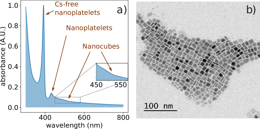
It turns out that these nanocubes, despite the fact that they are a side product of the synthesis, are very interesting for single photon emitters as we will show. In the following, we select only the PL from these cubes. Almost all the \chCsPbBr3 nanoplatelets are removed by centrifuging the solution as explained in methods. The obtained \chCsPbBr3 nanocubes appear to be more stable upon dilution that the one obtained by the direct procedure, as shown in the following.
2.1 Optical characterization
We optically characterized the NCs using an inverted confocal microscope: the experimental setup is shown in Figure 2a.
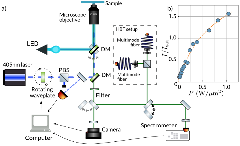
The samples are prepared for optical characterization measurements by spin-coating the colloidal solution on a glass coverslip. A LED lamp at is first used to locate the emitters and an image of the field of view of the microscope is collected by a CMOS camera. A single emitter is then excited via a picosecond pulsed laser (pulse width ) with a repetition rate adjustable from to . After filtering out the excitation wavelength, the luminescence of a single perovskite nanocube is collected by an inverted confocal microscope and sent to the optical characterization part. All the measurements were performed at room temperature.
A typical emission spectrum is reported in Figure 3a and shows a central wavelength of with a full width at half maximum (FWHM) of about . The distribution of the emitted wavelengths with the corresponding FWHM is shown in Figure 3b for 78 emitters.
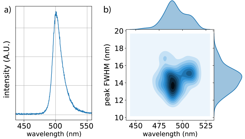
Here, we clearly see two main peaks with central emission wavelength (CEW) at and respectively. The mean FWHM of the emitted light is about for the first peak and for the second one. By comparison with the bulk perovskite emission wavelength at about 24, 25, 26, we attribute the former emission to small single photon emitters NCs with slight quantum confinement and the latter emission to large size nanocubes for which the confinement is mostly absent. As shown in the following, the small size nanocubes exhibit strongly antibunched emission, highlighting for the first time in this kind of emitters the crucial role of the charge confinement on their quantum properties. We report a study over 24 different emitters. For each emitter we measured the emitted power as a function of the excitation intensity. The background is subtracted from the experimental data. By fitting the data using the following saturation function, we are able to extract the saturation intensity :
| (1) |
The first term of the sum represents the saturating part due to the single exciton component while the second is due to bi-exciton emission27, 8, 28. Specifically is the saturation intensity while and depend on the intensity of single and bi-exciton components of the emission.
A typical saturation curve is shown in Figure 2b. To minimize the effect of the blinking on the data analysis, multiple measurements are taken for each experimental intensity in the graph, and only the one with the strongest emission is kept. We observed a median of . The presence of a bi-exciton component indicates that the correlation function will depend on the intensity at which we excite the emitters. We clearly observed this behavior when repeating the measurements for several excitation intensities. To perform reliable measurements on several emitters and to ensure a signal well above the noise level, we performed all the measurements at the saturation intensity.
2.2 Effect of the sample dilution on the photobleaching
Usually perovskite nanocrystals at room temperature suffer from fast photo-bleaching when they are exposed to light. Several studies presented lead halide perovkites NCs emission instability29. Often, the monitoring of the spectral stability over few minutes is used to evaluate the photo-stability28, 8, showing that the CEW shifts to more than after few tens of seconds for perovkite nanocrystals directly deposited on a glass-plate. Even when they are encapsulated with polystyrene, the longest measurement time recorded in the literature by Rainò et al.8 was around . The observed spectral drift has been attributed to the degradation of the nanocrystals, resulting in a progressive reduction of their sizes. In our case, the study of the photo-stability of the sample synthesized with the procedure described above shows a significant improvement of the photostability of the emitters under illumination.
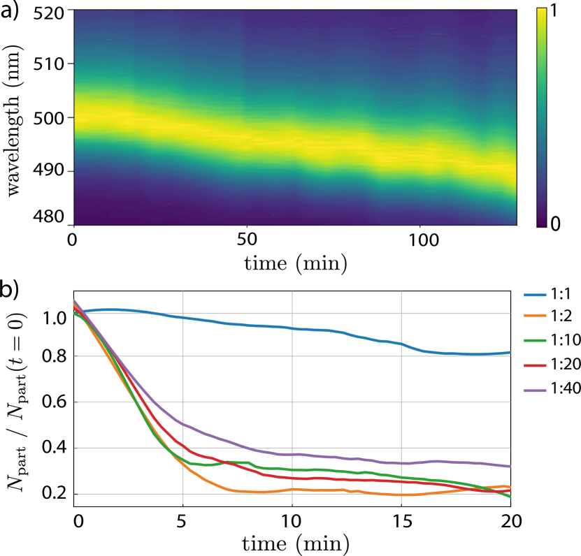
We prepared six samples using different dilutions starting from the most concentrated solution (typically with a molar concentration between -), up to a dilution of 1:100, using toluene as solvent. We started by analyzing the highest concentration sample. With this concentration value, we are still able to individually address each emitter and to collect its luminescence for more than with strongly reduced bleaching effects. This can be clearly see in Figure 4a: an emitter is excited for while its emission spectrum is collected every . The figure reports the evolution of the normalized emission spectra versus time. A blue-shift is observed, as already reported by Rainò et al.8, but on a much longer time scale: indeed our emitters exhibit a blue-shift of less than after two hours, showing a remarkable stability, two orders of magnitude better than previously observed5, 8. To the best of our knowledge, it is one of the most robust samples reported in the literature.
This robustness is strongly related to the concentration of the emitters in the solution, and drops fast when we dilute the sample. Our final objective is to couple a single emitter to a tapered optical nanofiber to develop an integrated singe photon source. For this, we need to use a strongly diluted sample. It is then crucial to investigate the behavior of the emitters as a function of the concentration.
The results of a systematic study of the effect of the dilution are reported in Figure 4b where each sample is strongly illuminated with light from the LED lamp while a video of the sample emission is recorded. Analyzing each frame of the video (we take a frame each 20 seconds) we can estimate the number of NCs that are still emitting from the first frame. We can clearly see that only the concentrated sample (so-called (1:1)) lasts for a long time with more than of the emitters still working after , while for all the other samples (from dilutions (1:2) to (1:100)) half of the emitters have bleached after . We attribute this effect to the dynamic bonding of the ligand to the perovskite nanocrystal surface. Under dilute conditions, the free ligands can hardly find the surface of another nanocrystal. This displaces the equilibrium between bound and unbound ligands towards the latter. As a result, the dilution process leads to poorly passivated nanocrystals which can easily bleach.
2.3 Blinking characterization
The emitted intensity of a NC is not constant in time but tends to fluctuate: this phenomenon is known as blinking. This behavior has been reported for several kinds of quantum emitters such as single molecules30, 31, \chSi nanocrystals32 and \chCdSe/\chCdS colloidal quantum dots33, 34, 35, 36, 37, 38.
Usually the fluorescence blinking is attributed to the trapping of charge carriers. In particular, it has been shown that we can distinguish two types of blinking: Type A, in which the core is left effectively charged and the low fluorescence state is caused by the recombination due to the Auger effect, and Type B, in which the trapped charge can recombine non-radiatively with its opposite charge and the blinking is due to fluctuations in the trapping rate.
A well established method to experimentally distinguish between Type A and Type B blinking is to study the spontaneous emission lifetime dependence on the emission intensity: in Type A blinking the lifetime is expected to depend on the emission intensity39 while in Type B the lifetime should not depend on the intensity39, 40.
When the typical blinking time is too short with respect to the chosen binning of the time-trace curve, it becomes impossible to completely distinguish between grey and bright states: in this case it is more appropriate to describe the behavior of the emitter in terms of flickering 39.
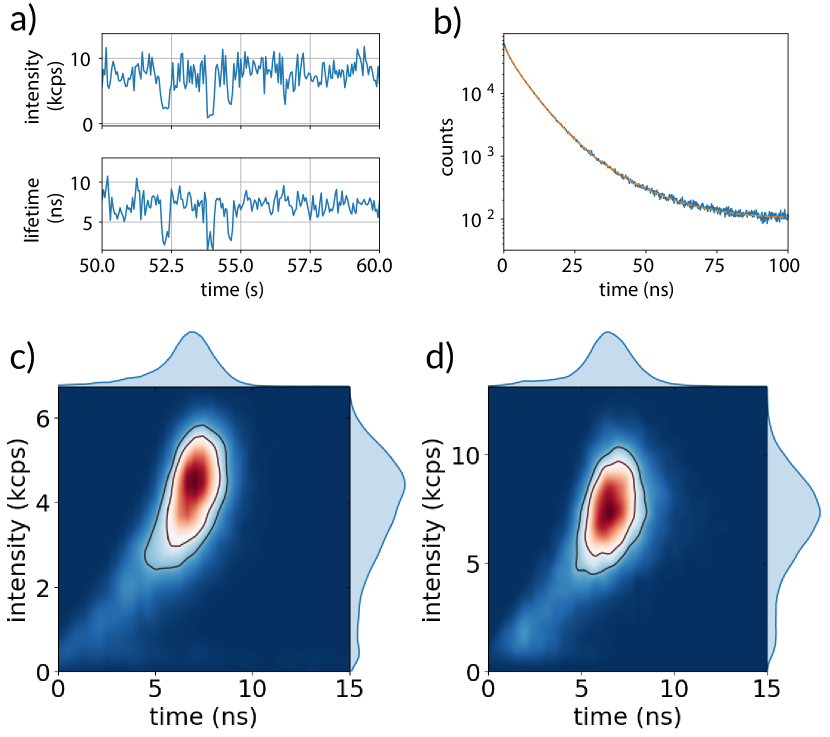
Our emitters, like the vast majority of perovskite NCs reported in the literature41, 42, show a clear flickering behavior in their emission time trace. A zoom of a typical blinking trace (i.e.the emitted intensity as a function of time) of one emitter is shown in the upper box of Figure 5a. The signal is binned with a binning time of . The complete blinking trace is reported in the supplementary information. Interestingly, the inspection of this trace indicate a reduced blinking with respect to the typical behavior of this kind of perovskites reported in literature 5. In the lower box of Figure 5a the mean lifetime versus time is reported: a clear correlation between the two curves is observable which indicates the presence of a type A blinking for these emitters.
In order to perform a more quantitative analysis, we fit the lifetime histogram with a triple-exponential decay model:
| (2) |
with three different lifetimes, , and , corresponding to the neutral, the charged, and the biexciton state emission respectively39. In equation (2) represents the pulse arrival time, while are the amplitudes of each decay component; B is an offset added to take into account the dark counts. A typical result of the fitting procedure is shown in Figure 5b, showing a good agreement with the experimental results. The dependence of the lifetime on the emitted intensity is commonly studied 39, 5, 43 by using the fluorescence lifetime-intensity distribution (FLID). In Figure 5c and 5d two FLIDs images corresponding to the same NC are shown, corresponding to an excitation intensity of and respectively, obtained with a bin size of . The dark curves delimit an area corresponding respectively to 50% (inner one) and 68% (outer one) probability of emission. As opposed to previous reports5, showing a predominance of the grey state emission for high excitation powers, with a significant decrease of the emission intensity, remarkably, our perovskite nanocubes remain in the same proportion of bright and grey state while excited up to and more, without any significant decrease of the emission intensity.
2.4 Quantum properties
To characterize the quantum emission and verify if our NCs can be used as single photon emitters, we measured the autocorrelation function using a Hanbury Brown and Twiss (HBT) setup (see Figure 2). The autocorrelation function is defined as follows:
where is the intensity of the emission, the time and the delay between two different photon arrivals.
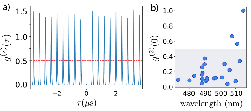
Experimentally the beam is divided in two parts by a 50/50 beam splitter (see Figure 2a) and sent to two avalanche photodiode single photon detectors (APDs). We record the arrival times with the time tagged time-resolved44 method. We then create a histogram of the relative arrival times of the photons with a time bin of , shown in figure 6a. Due to the blinking effect, the peaks close to the delay peak are higher than 45; on the other hand the peaks of the autocorrelation function tend to 1 for large delays compared to the characteristics blinking time. The histogram is thus normalized by setting the mean height of the peaks with to be . This procedure is well established and documented in literature46, 47. The background, mainly given by the dark counts of the APDs, is subtracted following the procedure described in supplementary materials.
The at delay is according to Figure 6a, well below showing clear signature of a single photon emission. We found that of our emitters show a very good single photon emission, with .
We perform a statistical analysis of the as a function of the central emission wavelength, shown in Figure 6b. We observe a clear degradation of the single photon emission for longer wavelengths. In particular, for CEWs above , the autocorrelation function value is always higher than , indicating that the single photon emission is lost. The reason for that is that for the biggest NCs the quantum confinement is no longer effective and this has the effect to increase the emission wavelength and to reduce the quality of the single photon emission.
3 Nanofiber integration
In this section, we describe the first realization of the coupling of a single perovskite nanocube with an optical taperd nanofiber, constituting a prototype of an interesting hybrid nanophotonic device for quantum technologies-oriented applications. Tapered nanofibers are photonic waveguides obtained by stretching a standard optical fiber while heating it, in order to reduce its diameter to some hundreds of nanometers. This results in a strong evanescent field in the vicinity of the fiber48, which enables the coupling of the light emitted by a nano-emitter located nearby directly into the nanofiber thus obtaining a compact and integrated single photon source49. This approach has been demonstrated with single atoms12, 13 as well as single colloidal quantum dots14, 15, 16 or with nanodiamonds containing single defects17. This is of great interest for quantum applications, where nanofiber-based systems are rapidly developing50.
In order to couple our NCs to the nanofiber, we place on top of it a droplet with a dilution 1:100 of the original solution in toluene using a micropipette. We then use a translation stage to carefully approach and eventually touch the nanofiber with the droplet, while monitoring the movement with a microscope. This is a critical step, as the nanofiber can easily break. When successful, this procedure results in several emitters deposited onto the nanofiber.
The setup used for this study is shown in Figure 7.
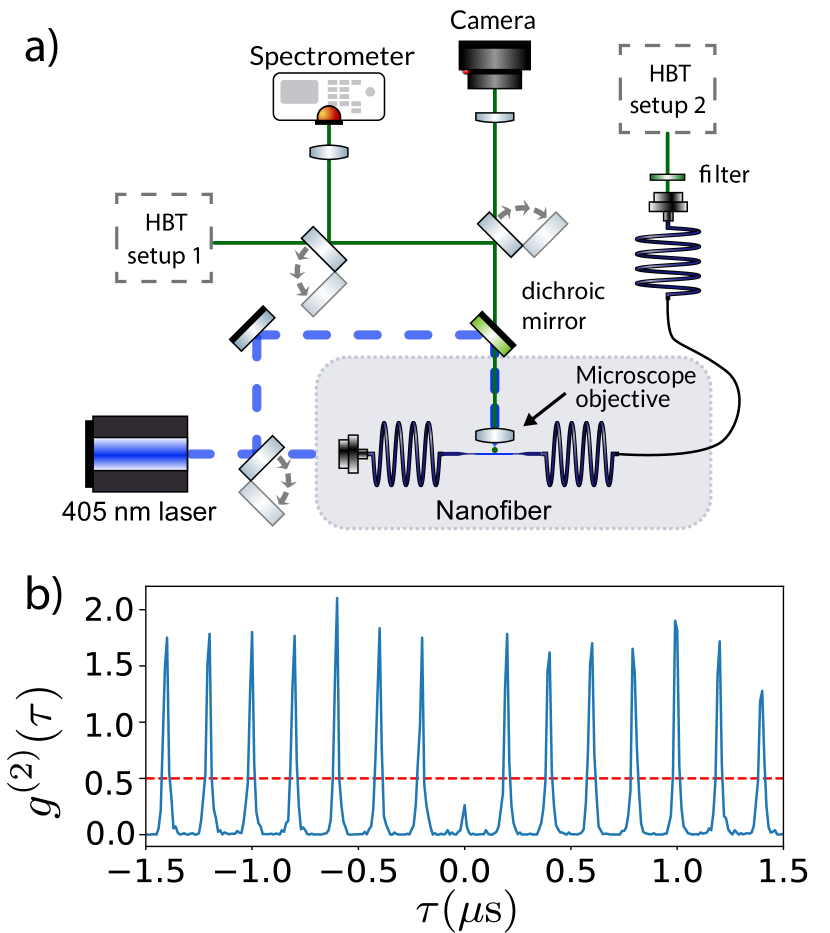
We firstly select the emitter sending the laser in the fiber and detect the photoluminescence from the microscope objective. Then, we excite a single NC located on top of the nanofiber with a laser sent through that microscope objective. A significant fraction of the emitted light is coupled into the nanofiber and propagates to its end. The end of the fiber is plugged to an HBT set-up for a measurement following the procedure previously described. Optionally, photon antibunching and spectral measurements can be performed also in free-space via the light collected with the microscope objective. A typical antibunching measurement performed on the light collected via the nanofiber is shown in Figure 7. We are still able to detect single photon emission, and this demonstrates that a single perovskite NC is coupled to a nanofiber and emits single photons directly inside it. These results show that our NCs are not damaged by the deposition process and validate this approach for this kind of sources, that, due to the dilution, can be used for some minutes once deposited over the nanofiber. Due to the versatility of the perovskite nanocubes and to their emission of single photons with long coherence time2, this technique opens the way to the realization of nanofiber-based, compact, integrated hybrid devices for indistinguishable single photon generation with solid state emitters. In order to achieve this final goal, it is crucial to further improve the stability of the emitters thanks to a deeper understanding of the role that ligands and dilution play on their robustness.
4 Conclusions
We investigated the properties of highly-stable \chCsPbBr3 nanocrystals as single photon emitters. The effect of the dilution on the photo-stability was investigated, confirming a degradation when increasing the dilution. To further improve the stability, a promising approach, currently under investigation, is based on a better ligand control in order to increase the dilution without breaking the equilibrium of the colloidal solution.
A full characterization of the optical properties of these emitters was performed, highlighting the role of the charge confinement in their antibunching behaviour. A deep analysis of the blinking and single photon emission of perovskite nanocubes were presented, showing a strongly reduced blinking and a remarkable stability of the bright state emission as a function of the excitation power. This feature guarantees a very low also for high excitation power. Moreover, for the first time with such emitters, we have shown the coupling of a single perovskite nanocube with a tapered optical nanofiber. Thanks to the near-field interaction, single photons are emitted in the near field of the nanofiber demonstrating the proof of principle of a compact, integrated single photon source. The coupling to other platforms, such as the ion-integrated waveguides one51, is also envisioned to obtain integrated single photon sources for quantum photonic applications.
5 Experimental
5.0.1 Chemicals
PbBr2 (Alfa Aesar, ), \chCs2CO3 (Alfa aesar, ), oleylamine (OLA, Acros, ), oleic acid (OA, Sigma-Aldrich), octylamine (Oct.Am, Alfa aesar, ), Octanoic acid (Oct.Acid, Acros, ), octadecene (ODE, Acros Organics, ), toluene (VWR, rectapur).
5.0.2 Caesium oleate precursor
We mix in a three neck flask, of \chCs2CO3 in of ODE and of OA. The content of the flask is stirred and degased under vacuum at room temperature for . The flask is heated at for . The atmosphere is switched to nitrogen and the temperature raised to . The reaction is carried on for . At this stage the salt is fully dissolved. The temperature is cooled down below and the falsk degased under vacuum. Finally this solution is used as a stock solution.
5.0.3 Nanocrystal synthesis
In a three neck flask, of \chPbBr2 is mixed in of ODE. The flask is degased under vacuum at room temperature for . Then, the temperature is raised to . At , of OLA is injected. Once vacuum has recovered, of OA is injected. After 5 min, of oct.Am is injected. Once the vacuum has recovered, of oct.Acid is injected. The solution is colorless at this stage. The solution is further degased at for . The atmosphere is switched to nitrogen and the temperature raised to . Around of CsOA solution is injected, and the solution turns turbid. The solution is conducted for and finally quickly cooled down by removing the heating mantle and using a water bath. The solution is transferred to plastic tube and centrifuged. The supernatant is discarded. The pellet is dispersed in of toluene. The solution is centrifuged again at low speed ( for ). The pellet is discarded and the colloidally stable supernatant is stored.
5.0.4 Material characterization
UV-visible absorption spectrum are obtained by diluting the nanoparticles in hexane and using a JASCO V730 spectrometer. For transmission electron microscopy, a dilute solution of nanocrystals is drop-casted onto a copper grid coated with a thin amorphous carbon layer. The grid is then degased under secondary vacuum overnight. Imaging was conducted with a JEOL 2010 microscope operated at .
The project is supported by ERC starting grant blackQD (grant n° 756225), by ANR grants IPER-Nano2 (ANR-18CE30-0023-01), Copin (ANR-19-CE24-0022), Frontal (ANR-19-CE09-0017), Graskop (ANR-19-CE09-0026) and by the European Union’s Horizon 2020 research and innovation program under grant agreement No 828972 -Nanobright. AB and QG are members of the Institut Universitaire de France (IUF). The authors thank J.-P. Hermier for inspiring discussions.
Supporting information available: Integral fluorescence trace, procedure for FLID generation, noise cleaning procedure for measurements, procedure for NCs deposition on nanofibers. This material is available free of charge via the internet at \urlhttp://pubs.acs.org
References
- Park 2015 Park, N.-G. Perovskite solar cells: an emerging photovoltaic technology. Materials today 2015, 18, 65–72
- Utzat et al. 2019 Utzat, H.; Sun, W.; Kaplan, A. E. K.; Krieg, F.; Ginterseder, M.; Spokoyny, B.; Klein, N. D.; Shulenberger, K. E.; Perkinson, C. F.; Kovalenko, M. V. et al. Coherent Single-Photon Emission from Colloidal Lead Halide Perovskite Quantum Dots. Science 2019, 363, 1068–1072
- Rainò et al. 2016 Rainò, G.; Nedelcu, G.; Protesescu, L.; Bodnarchuk, M. I.; Kovalenko, M. V.; Mahrt, R. F.; Stöferle, T. Single Cesium Lead Halide Perovskite Nanocrystals at Low Temperature: Fast Single-Photon Emission, Reduced Blinking, and Exciton Fine Structure. ACS Nano 2016, 10, 2485–2490
- Huo et al. 2020 Huo, C.; Fong, C. F.; Amara, M.-R.; Huang, Y.; Chen, B.; Zhang, H.; Guo, L.; Li, H.; Huang, W.; Diederichs, C. et al. Optical Spectroscopy of Single Colloidal \chCsPbBr3 Perovskite Nanoplatelets. Nano Letters 2020,
- Park et al. 2015 Park, Y.-S.; Guo, S.; Makarov, N. S.; Klimov, V. I. Room Temperature Single-Photon Emission from Individual Perovskite Quantum Dots. ACS Nano 2015, 9, 10386–10393
- Rainò et al. 2018 Rainò, G.; Becker, M. A.; Bodnarchuk, M. I.; Mahrt, R. F.; Kovalenko, M. V.; Stöferle, T. Superfluorescence from Lead Halide Perovskite Quantum Dot Superlattices. Nature 2018, 563, 671–675
- Chen et al. 2019 Chen, L.-C.; Tien, C.-H.; Tseng, Z.-L.; Dong, Y.-S.; Yang, S. Influence of PMMA on All-Inorganic Halide Perovskite \chCsPbBr3 Quantum Dots Combined with Polymer Matrix. Materials 2019, 12, 985
- Rainò et al. 2019 Rainò, G.; Landuyt, A.; Krieg, F.; Bernasconi, C.; Ochsenbein, S. T.; Dirin, D. N.; Bodnarchuk, M. I.; Kovalenko, M. V. Underestimated Effect of a Polymer Matrix on the Light Emission of Single \chCsPbBr3 Nanocrystals. Nano Letters 2019, 19, 3648–3653
- Saris et al. 2019 Saris, S.; Dona, S.; Niemann, V.; Loiudice, A.; Buonsanti, R. Optimizing the Atomic Layer Deposition of Alumina on Perovskite Nanocrystal Films by Using \chO2 as a Molecular Probe. ChemRxiv 2019,
- Xiang et al. 2018 Xiang, Q.; Zhou, B.; Cao, K.; Wen, Y.; Li, Y.; Wang, Z.; Jiang, C.; Shan, B.; Chen, R. Bottom up Stabilization of \chCsPbBr3 Quantum Dots-Silica Sphere with Selective Surface Passivation via Atomic Layer Deposition. Chemistry of Materials 2018, 30, 8486–8494
- Pan et al. 2015 Pan, J.; Sarmah, S. P.; Murali, B.; Dursun, I.; Peng, W.; Parida, M. R.; Liu, J.; Sinatra, L.; Alyami, N.; Zhao, C. et al. Air-Stable Surface-Passivated Perovskite Quantum Dots for Ultra-Robust, Single- and Two-Photon-Induced Amplified Spontaneous Emission. The Journal of Physical Chemistry Letters 2015, 6, 5027–5033
- Le Kien et al. 2005 Le Kien, F.; Gupta, S. D.; Balykin, V.; Hakuta, K. Spontaneous emission of a cesium atom near a nanofiber: Efficient coupling of light to guided modes. Physical Review A 2005, 72, 032509
- Klimov and Ducloy 2004 Klimov, V.; Ducloy, M. Spontaneous emission rate of an excited atom placed near a nanofiber. Physical Review A 2004, 69, 013812
- Fujiwara et al. 2011 Fujiwara, M.; Toubaru, K.; Noda, T.; Zhao, H.-Q.; Takeuchi, S. Highly efficient coupling of photons from nanoemitters into single-mode optical fibers. Nano letters 2011, 11, 4362–4365
- Yalla et al. 2012 Yalla, R.; Nayak, K.; Hakuta, K. Fluorescence photon measurements from single quantum dots on an optical nanofiber. Optics express 2012, 20, 2932–2941
- Joos et al. 2018 Joos, M.; Ding, C.; Loo, V.; Blanquer, G.; Giacobino, E.; Bramati, A.; Krachmalnicoff, V.; Glorieux, Q. Polarization control of linear dipole radiation using an optical nanofiber. Physical Review Applied 2018, 9, 064035
- Vorobyov et al. 2016 Vorobyov, V. V.; Soshenko, V. V.; Bolshedvorskii, S. V.; Javadzade, J.; Lebedev, N.; Smolyaninov, A. N.; Sorokin, V. N.; Akimov, A. V. Coupling of Single NV Center to Adiabatically Tapered Opticalsingle Mode Fiber. The European Physical Journal D 2016, 70, 269
- Protesescu et al. 2015 Protesescu, L.; Yakunin, S.; Bodnarchuk, M. I.; Krieg, F.; Caputo, R.; Hendon, C. H.; Yang, R. X.; Walsh, A.; Kovalenko, M. V. Nanocrystals of cesium lead halide perovskites (\chCsPbX3, X= Cl, Br, and I): novel optoelectronic materials showing bright emission with wide color gamut. Nano letters 2015, 15, 3692–3696
- De Roo et al. 2016 De Roo, J.; Ibáñez, M.; Geiregat, P.; Nedelcu, G.; Walravens, W.; Maes, J.; Martins, J. C.; Van Driessche, I.; Kovalenko, M. V.; Hens, Z. Highly dynamic ligand binding and light absorption coefficient of cesium lead bromide perovskite nanocrystals. ACS nano 2016, 10, 2071–2081
- Krieg et al. 2019 Krieg, F.; Ong, Q. K.; Burian, M.; Rainò, G.; Naumenko, D.; Amenitsch, H.; Süess, A.; Grotevent, M. J.; Krumeich, F.; Bodnarchuk, M. I. et al. Stable Ultraconcentrated and Ultradilute Colloids of \chCsPbX3 (X= Cl, Br) Nanocrystals Using Natural Lecithin as a Capping Ligand. Journal of the American Chemical Society 2019, 141, 19839–19849
- Zhang et al. 2019 Zhang, B.; Goldoni, L.; Zito, J.; Dang, Z.; Almeida, G.; Zaccaria, F.; De Wit, J.; Infante, I.; De Trizio, L.; Manna, L. Alkyl phosphonic acids deliver \chCsPbBr3 Nanocrystals with high photoluminescence quantum yield and truncated octahedron shape. Chemistry of Materials 2019, 31, 9140–9147
- Liu et al. 2019 Liu, Y.; Siron, M.; Lu, D.; Yang, J.; dos Reis, R.; Cui, F.; Gao, M.; Lai, M.; Lin, J.; Kong, Q. et al. Self-Assembly of Two-Dimensional Perovskite Nanosheet Building Blocks into Ordered Ruddlesden–Popper Perovskite Phase. Journal of the American Chemical Society 2019, 141, 13028–13032
- Weidman et al. 2016 Weidman, M. C.; Seitz, M.; Stranks, S. D.; Tisdale, W. A. Highly tunable colloidal perovskite nanoplatelets through variable cation, metal, and halide composition. ACS nano 2016, 10, 7830–7839
- Mannino et al. 2020 Mannino, G.; Deretzis, I.; Smecca, E.; La Magna, A.; Alberti, A.; Ceratti, D.; Cahen, D. Temperature-Dependent Optical Band Gap in CsPbBr3, MAPbBr3, and FAPbBr3 Single Crystals. The Journal of Physical Chemistry Letters 2020, 11, 2490–2496
- Liashenko et al. 2019 Liashenko, T. G.; Cherotchenko, E. D.; Pushkarev, A. P.; Pakštas, V.; Naujokaitis, A.; Khubezhov, S. A.; Polozkov, R. G.; Agapev, K. B.; Zakhidov, A. A.; Shelykh, I. A. et al. Electronic structure of CsPbBr 3- x Cl x perovskites: synthesis, experimental characterization, and DFT simulations. Physical Chemistry Chemical Physics 2019, 21, 18930–18938
- Ng et al. 2018 Ng, C. H.; Ripolles, T. S.; Hamada, K.; Teo, S. H.; Lim, H. N.; Bisquert, J.; Hayase, S. Tunable open circuit voltage by engineering inorganic cesium lead bromide/iodide perovskite solar cells. Scientific reports 2018, 8, 1–9
- Park et al. 2011 Park, Y.-S.; Malko, A. V.; Vela, J.; Chen, Y.; Ghosh, Y.; García-Santamaría, F.; Hollingsworth, J. A.; Klimov, V. I.; Htoon, H. Near-unity quantum yields of biexciton emission from CdSe/CdS nanocrystals measured using single-particle spectroscopy. Physical review letters 2011, 106, 187401
- Raja et al. 2016 Raja, S. N.; Bekenstein, Y.; Koc, M. A.; Fischer, S.; Zhang, D.; Lin, L.; Ritchie, R. O.; Yang, P.; Alivisatos, A. P. Encapsulation of Perovskite Nanocrystals into Macroscale Polymer Matrices: Enhanced Stability and Polarization. ACS Applied Materials & Interfaces 2016, 8, 35523–35533
- Huang et al. 2017 Huang, H.; Bodnarchuk, M. I.; Kershaw, S. V.; Kovalenko, M. V.; Rogach, A. L. Lead Halide Perovskite Nanocrystals in the Research Spotlight: Stability and Defect Tolerance. ACS Energy Letters 2017, 2, 2071–2083
- Yip et al. 1998 Yip, W.-T.; Hu, D.; Yu, J.; Vanden Bout, D. A.; Barbara, P. F. Classifying the Photophysical Dynamics of Single- and Multiple-Chromophoric Molecules by Single Molecule Spectroscopy. The Journal of Physical Chemistry A 1998, 102, 7564–7575
- Dickson et al. 1997 Dickson, R. M.; Cubitt, A. B.; Tsien, R. Y.; Moerner, W. E. On/off Blinking and Switching Behaviour of Single Molecules of Green Fluorescent Protein. Nature 1997, 388, 355–358
- Mason et al. 1998 Mason, M. D.; Credo, G. M.; Weston, K. D.; Buratto, S. K. Luminescence of Individual Porous Si Chromophores. Physical Review Letters 1998, 80, 5405–5408
- Nirmal et al. 1996 Nirmal, M.; Dabbousi, B. O.; Bawendi, M. G.; Macklin, J. J.; Trautman, J. K.; Harris, T. D.; Brus, L. E. Fluorescence Intermittency in Single Cadmium Selenide Nanocrystals. Nature 1996, 383, 802–804
- Shimizu et al. 2001 Shimizu, K. T.; Neuhauser, R. G.; Leatherdale, C. A.; Empedocles, S. A.; Woo, W. K.; Bawendi, M. G. Blinking Statistics in Single Semiconductor Nanocrystal Quantum Dots. Physical Review B 2001, 63, 205316
- Tang and Marcus 2005 Tang, J.; Marcus, R. A. Single Particle versus Ensemble Average: From Power-Law Intermittency of a Single Quantum Dot to Quasistretched Exponential Fluorescence Decay of an Ensemble. The Journal of Chemical Physics 2005, 123, 204511
- Peterson and Nesbitt 2009 Peterson, J. J.; Nesbitt, D. J. Modified Power Law Behavior in Quantum Dot Blinking: A Novel Role for Biexcitons and Auger Ionization. Nano Letters 2009, 9, 338–345
- Mahler et al. 2008 Mahler, B.; Spinicelli, P.; Buil, S.; Quelin, X.; Hermier, J.-P.; Dubertret, B. Towards Non-Blinking Colloidal Quantum Dots. Nature Materials 2008, 7, 659–664
- Houel et al. 2015 Houel, J.; Doan, Q. T.; Cajgfinger, T.; Ledoux, G.; Amans, D.; Aubret, A.; Dominjon, A.; Ferriol, S.; Barbier, R.; Nasilowski, M. et al. Autocorrelation Analysis for the Unbiased Determination of Power-Law Exponents in Single-Quantum-Dot Blinking. ACS Nano 2015, 9, 886–893
- Galland et al. 2011 Galland, C.; Ghosh, Y.; Steinbrück, A.; Sykora, M.; Hollingsworth, J. A.; Klimov, V. I.; Htoon, H. Two types of luminescence blinking revealed by spectroelectrochemistry of single quantum dots. Nature 2011, 479, 203–207
- Brawand et al. 2015 Brawand, N. P.; Vörös, M.; Galli, G. Surface Dangling Bonds Are a Cause of B-Type Blinking in Si Nanoparticles. Nanoscale 2015, 7, 3737–3744
- Trinh et al. 2018 Trinh, C. T.; Minh, D. N.; Ahn, K. J.; Kang, Y.; Lee, K.-G. Organic–Inorganic \chFAPbBr3 Perovskite Quantum Dots as a Quantum Light Source: Single-Photon Emission and Blinking Behaviors. ACS Photonics 2018, 5, 4937–4943
- Seth et al. 2016 Seth, S.; Mondal, N.; Patra, S.; Samanta, A. Fluorescence Blinking and Photoactivation of All-Inorganic Perovskite Nanocrystals \chCsPbBr3 and \chCsPbBr2I. The Journal of Physical Chemistry Letters 2016, 7, 266–271
- Hu et al. 2015 Hu, F.; Cao, Z.; Zhang, C.; Wang, X.; Xiao, M. Defect-Induced Photoluminescence Blinking of Single Epitaxial InGaAs Quantum Dots. Scientific Reports 2015, 5, 1–6
- Wahl and Orthaus-Müller 2014 Wahl, M.; Orthaus-Müller, S. Time tagged time-resolved fluorescence data collection in life sciences. technical note, PicoQuant GmbH 2014,
- Manceau et al. 2018 Manceau, M.; Vezzoli, S.; Glorieux, Q.; Giacobino, E.; Carbone, L.; De Vittorio, M.; Hermier, J.-P.; Bramati, A. CdSe/CdS Dot-in-Rods Nanocrystals Fast Blinking Dynamics. ChemPhysChem 2018, 19, 3288–3295
- Pierini et al. 2020 Pierini, S.; D’Amato, M.; Joos, M.; Glorieux, Q.; Giacobino, E.; Lhuillier, E.; Couteau, C.; Bramati, A. Hybrid Device for Quantum Nanophotonics. arXiv:2001.10480 [physics, physics:quant-ph] 2020,
- Manceau et al. 2014 Manceau, M.; Vezzoli, S.; Glorieux, Q.; Pisanello, F.; Giacobino, E.; Carbone, L.; De Vittorio, M.; Bramati, A. Effect of charging on CdSe/CdS dot-in-rods single-photon emission. Physical Review B 2014, 90, 035311
- Le Kien et al. 2004 Le Kien, F.; Liang, J. Q.; Hakuta, K.; Balykin, V. I. Field Intensity Distributions and Polarization Orientations in a Vacuum-Clad Subwavelength-Diameter Optical Fiber. Optics Communications 2004, 242, 445–455
- Joos et al. 2019 Joos, M.; Bramati, A.; Glorieux, Q. Complete polarization control for a nanofiber waveguide using the scattering properties. Optics express 2019, 27, 18818–18830
- Nayak et al. 2018 Nayak, K. P.; Sadgrove, M.; Yalla, R.; Le Kien, F.; Hakuta, K. Nanofiber quantum photonics. Journal of Optics 2018, 20, 073001
- Madrigal et al. 2016 Madrigal, J. B.; Tellez-Limon, R.; Gardillou, F.; Barbier, D.; Geng, W.; Couteau, C.; Salas-Montiel, R.; Blaize, S. Hybrid integrated optical waveguides in glass for enhanced visible photoluminescence of nanoemitters. Applied optics 2016, 55, 10263–10268