Long-range influence of manipulating disordered-insulators locally
Abstract
Localization of wavefunctions is arguably the most familiar effect of disorder in quantum systems. It has been recently argued [V. Khemani, R. Nandkishore, and S. L. Sondhi, Nature Physics, 11, 560 (2015)] that, contrary to naive expectation, manipulation of a localized-site in the disordered medium may produce a disturbance over a length-scale much larger than the localization-length, . Here we report on the observation of this nonlocal phenomenon in electronic transport experiment. Being a wave property, visibility of this effect hinges upon quantum-coherence, and its spatial-scale may be ultimately limited by the phase-coherent length of the disordered insulator. Evidence for quantum coherence in the Anderson-insulating phase may be obtained from magneto-resistance measurements which however are useful mainly in thin-films. The technique used in this work offers an empirical method to measure this fundamental aspect of Anderson-insulators even in relatively thick samples.
I Introduction
Disorder may lead to a variety of non-trivial phenomena in both classical and quantum systems. The most familiar of these phenomena is Anderson localization 1 . This phenomenon has been established in electronic transport 2 , propagation of light 3 and sound waves 4 , and in disordered Bose-Einstein condensates 5 .
Localization of wavefunctions may seem a way to allow manipulation of a particular site in a solid while parts of the system that are remote from it are unaffected. This expectation has been recently questioned; Khemani, Nandkishore, and Sondhi (KNS) 6 shown that adiabatically changing the potential on a local site will produce an effect over a distance that may exceed by a considerable margin. This long-range effect may have important consequences for quantum-computing manipulations and for fundamental issues such as the orthogonality-catastrophe 6 ; 7 .
In this work we describe a method that allows observation of the KNS effect in an electronic system and show results that demonstrate the quantum nature of the phenomenon.
II Experimental
II.1 Sample preparation
The samples used in this study were amorphous indium-oxide (InO) made by e-gun evaporation of 99.999% pure InO onto room-temperature Si-wafers in a partial pressure of 1.3x10mBar of O and a rate of 0.30.1Å/s. Under these conditions the carrier-concentration N of the samples, measured by the Hall-Effect at room-temperatures, was N(10.1)x10cm. Using free-electron formula, this carrier-concentration is associated with n/10ergcm. The Si wafers (boron-doped with bulk resistivity 2x10cm) were employed as the gate-electrode in the field-effect experiments. A thermally-grown SiO layer, 2m thick, served as the spacer between the sample and the conducting Si:B substrate. Films thickness was measured in-situ by a quartz-crystal monitor calibrated against X-ray reflectometry. Samples geometry was defined by the use of stainless-steel mask during deposition into rectangular strips 0.80.1mm wide and 10.1mm long.
II.2 Measurement techniques
Conductivity of the samples was measured using a two-terminal ac technique employing a 1211 ITHACO current preamplifier and a PAR 124A lock-in amplifier using frequencies of 30-75Hz depending on the RC of the sample-gate structure. R is the source-drain resistance and C is the capacitance between the sample and the gate (C in our samples was typically 10F and R for the samples studied in this work ranged between 1.5-20M). Except when otherwise noted, the ac voltage bias in conductivity measurements was small enough to ensure near-ohmic conditions. Most measurements were performed with the samples immersed in liquid helium at T4.1K held by a 100 liters storage-dewar. This allowed up to two months measurements on a given sample while keeping it cold (and in the dark). These conditions are essential for measurements where extended times of relaxation processes are required at a constant temperature. All samples described below were Anderson-insulating and exhibited hopping conductivity that for 4T50K was of the Mott form 8 ;
| (1) |
as illustrated in Fig.1 for two typical samples.
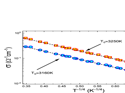
This allowed an estimate of the localization-length through 8 : kT(n/) where n/ is the thermodynamic density-of-states. With n/10ergcm, the values for the samples reported below ranged between 2.7nm to 3.3nm. These values are close to the inter-carrier distance Nof this version of InO as may be expected for samples that are far from the metal-insulating transition which applies to all our studied samples. This makes the estimate for , based on the (T) data, a plausible value.
Taking the sample far from equilibrium to study its thermalization dynamics is accomplished in this work by exposing the sample to an AlGaAs diode operating at 0.820.05m mounted on the sample-stage 10-15mm from the sample. The diode was energized by a computer-controlled Keithley 220 current-source. Upon exposure to the infrared source, the electrons are promptly raised to a high energy state and their excess energy is then dissipated into the phonon system (a radiation-less process 9 ). In this method, only the sample is efficiently heated and its excess energy is uniformly distributed throughout the sample much faster than the time-scale of the experiments described below. Full details of this technique and its application for the study of several Anderson insulators are described in 9 .
III Results and discussion
In a field-effect experiment, the charge Q added to the sample when the gate-voltage is changed by V, resides in a thin layer of thickness (4en/) at the interface between the sample and the spacer 10 ; 11 (The dielecric constant of the material is of the order of 10). The thickness of this layer in InO is 2nm, which is much smaller than the thickness d of the samples studied in this work that ranged between 45nm to 150nm. Yet, it turns out that the added charge Q to the system due to V had an effect extending over length-scales much longer than both and .
This observation may be inferred from G(V) plots, taken at different times tQ, while the sample is relaxing after being quench-cooled from an excited state; Consider the G(t,V) plots for the samples in Fig.2. The protocol used throughout the series of measurements shown in this composite figure was as follows. The sample, immersed in liquid He at T=4.11K, was exposed for 3 seconds to infra-red source (light-emitting-diode at 0.82 micron radiation) taking it from equilibrium. G(V) scans were then taken with constant V/t starting from V=0, at which the gate-voltage was kept between subsequent scans. These are labeled in the graphs by the time tQ that elapsed since turning off the infra-red source (and the onset of relaxation towards restoring equilibrium under V=0). Each of these G(V) plots reflects the energy dependence of n/ modulated by a ”memory-dip” which results from the interplay between disorder and Coulomb interaction 12 .
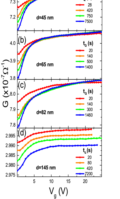
Note first the difference between the thinnest and thickest samples in the series, Fig.2a and 2d respectively. In the former, the G(V) plots taken at different times tend to merge for V10V while, for the 145 nm sample, they tend to become parallel.
A simple explanation to the results exhibited by the sample in Fig.2d is that the added charge only affects the part of the sample that is close to the spacer-interface while the rest of it is unaffected. In this case the sample is effectively composed of two conductors in parallel; one where the G(t,V) curves are like the pattern exhibited by the sample in Fig.2a, and another for which G(t) just monotonically decreases after the quantum-quench, independent of V. Superimposing these two components qualitatively reproduces the G(t,V) curves exhibited by the 145 nm sample in Fig.2d.
It is important to understand the different roles played by the infrared exposure versus the gate-sweeps in these experiments. Changing the gate-voltage or exposing the sample to infrared will take the system from equilibrium. However, these agents do not play a symmetric role in the protocol; the infrared exposure is a one-shot event driving the system far from equilibrium. Sweeping the gate is used to take a snapshot of how far the system is on its relaxation trail. This is done intermittently as time progresses and yields a certain swing G(t) reflecting the development of a memory dip. This G may be then compared with the background conductance-value that is going down with time due to the original excitation by the infrared source (which, as alluded to in section III, affects the entire thickness of the sample). The form of the observed G(t,V) plots will tell whether or not the gate-sweeping affects the entire sample volume (as in Fig.2a, 2b and 2c) or only part of it (as in Fig.2d).
The G(t,V) curves pattern characteristic of a thin sample has been first observed in 13 on crystalline indium-oxide and later in 14 on a different version of InO than the one used here (namely, with N8x10cm).
To account for the behavior of the three thinner samples is a more challenging task; apparently in these instances the disturbance caused by the added charge extends throughout their entire thickness - over a length-scale of d which, for the 82nm sample, is 25 to 30 times larger than the localization-length . It is hard to see how such a long-range effect is possible unless wavefunction-overlap that are L apart is much better than might be expected from exponential decay. The Coulomb interaction due to Q over this length-scale, even if unscreened, is too weak relative to the local disorder to affect G(V) during the time V is swept.
High transmission-channels through disordered media would offer an explanation for the long-range effect. These resonant channels are theoretically possible but exponentially rare 15 ; 16 ; 17 . By contrast, the scenario proposed by KNS creates such resonant channels in the disordered system with high probability by using a time-dependent adiabatic process 6 . Adapted for our geometry, quasi-extended states are parametrically formed perpendicular to the film plane by slowly varying the local potential V at the interface layer. As will be now shown, this scenario accounts for all aspects of the experimental results.
Let us first look at r, the extent of the ‘zone-of-disturbance’ expected of the KNS-produced resonances 6 :
| (2) |
With the value of the quenched-disorder in our samples 18 W0.5-1eV, rate of potential-change 19 V/t0.5meV/s, and 3nm Eq.1 gives r100nm.
Note that r100nm is consistent with our results (Fig.1); it is close to the film thickness below which the G(t,V) curves converge at high gate-voltages which implies rd. In addition, the mean values that V attains in the V-interval used in the experiments, covers the energy separation En·L for states that are apart by any L2. This secures ample ‘tuning-margin’ for creating the quasi-extended states by the KNS scenario.
A fundamental requirement on the KNS mechanism is that phase-coherence must be preserved throughout the spatial-scale in question. This requirement follows from the quantum-mechanical nature of the process. In other words, the range of disturbance may be r in Eq.1 only when Lϕ, the phase-coherent-length in the medium obeys Lϕr.
Evidence for phase-coherence in Anderson-localized films over scales of tens of several nano-meters has been reported. This evidence is based on two phenomena, both strictly requiring phase-coherence: orbital magneto-conductance 20 ; 21 , and Andreev tunneling 22 . The latter, performed on InO films of similar composition as used in the current work, demonstrated that a coherence-length of 60nm at T4K is realizable in this system.
A further test of the role of quantum-coherence in the nonlocal effect discussed here is to see how the G(t,V) plots change when dephasing is judiciously introduced. Once the dephasing-rate is large enough to cause Lϕd, the resulting G(t,V) plots should revert from the ‘converging’ pattern to that resembling the results in Fig.1d.
To implement this test in a controlled way, one needs a dephasing agent that can be turned on and off at will. An effective and easy to control mechanism for dephasing Anderson-insulators is using a non-ohmic field in the transport measurement 20 . This has been demonstrated in magneto-conductance measurements on strongly-localized indium-oxide films 20 . This technique was applied on three different InO samples and the results corroborate the expected behavior caused by the extra dephasing. Figure 3 illustrates the results of one of these experiments:
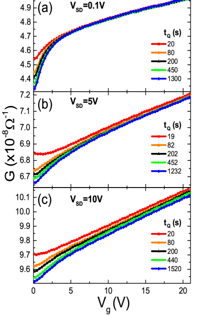
Figure 3a shows a set of G(t,V) curves taken in linear-response. These ‘converging’ plots are consistent with rd. Using non-ohmic V for measuring G(V) on the same sample produced however, different results; the G(t,V) curves (Fig.3b and 3c) resemble the pattern obtained for the thick sample in Fig.2d where presumably the range of V is smaller than the sample thickness.
Another indication that, under the higher V conditions, part of the sample is not affected by the gate-voltage is shown in Fig.4.
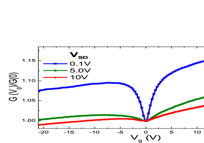
This figure compares the relative magnitude of the memory-dips taken under the same fields used in Fig.3a, 3b, and 3c. The figure shows a large reduction in the memory-dips magnitude for the two non-ohmic V used relative to the linear response plot. The reduced range of disturbance implied by the data in Fig.3b, 3c and 4 is consistent with the dephasing effect of non-ohmic fields causing Lϕ to become the shortest scale. Similar behavior was observed on two other samples with d=65nm and d=82nm upon application of non-ohmic fields.
For further discussion of the results of the non-ohmic fields, we show in Fig.5 resistance versus source-drain voltage V plots for three of the samples used in this study.
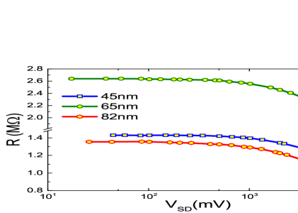
Note first that the increase in the overall conductance of the sample used in Fig.3 under V of 5V and 10V (by a factor of 1.5 and 2 respectively, see Fig.5 ) is not the reason for the qualitative change in the G(t,V) plots; when measured in linear-response, samples with the same d, but conductance that differed by as much as order of magnitude, still exhibited the same converging G(t,V) curves. Secondly, in terms of dephasing the effect of a non-ohmic field act in the same direction as higher sample temperature 20 . The increase of effective temperature T due to the applied source-drain field F may be roughly estimated as TeF/kwhich, for the F10Vmused in Fig.3c is tantamount to T0.1-0.3K.
That Lϕ in an Anderson-insulator may be 82nm at T4K, implicit to our proposed picture, is not an obvious fact, it deserves some elaboration; To put things in perspective, Lϕ of this order of magnitude is typical of diffusive samples at this temperature 23 . This may conflict with common intuition expecting disorder to decrease transport-related spatial-scales. However the dependence of Lϕ on disorder is not clear even in diffusive systems despite extensive studies 24 , let alone in the more intricate Anderson-insulating phase where this issue has barely been studied. On the basis of current knowledge it is not impossible that Lϕ in the insulating phase be as large as in the metallic phase. In terms of mechanisms, the insulating phase may even have an advantage; electron-electron inelastic scattering that, at low temperatures, is the main source of dephasing in diffusive systems, is suppressed in the insulating phase. This has been anticipated on theoretical grounds 24 , and was shown experimentally 25 . Moreover, the electron-phonon inelastic rate is likely also suppressed due to the reduced overlap between the initial and final electronic states involved in the inelastic event. Therefore dephasing due to inelastic scattering may actually be weakened in the strongly-localized regime. On the other hand, once interactions are turned on, a potential source for dephasing appears that may not have existed in the weak-disorder regime - spin-flips. This mechanism may become important once the on-site Coulomb repulsion is strong enough to precipitate a finite density of singly-occupied states at the Fermi-energy 26 . These singly-occupied sites act like local magnetic impurities and may contribute to dephasing 27 . This potential source of dephasing may be the reason for the paucity of experiments reporting on quantum-interference effects in Anderson insulators in systems that do exhibit such effects in their diffusive regime. Evidence for quantum-coherent effects is usually based on observation of anisotropic magneto-conductance. This technique however becomes ineffective for films thicker than few tens of a nanometer 21 , a weakness not shared by our protocol.
In sum, we demonstrated the existence of a nonlocal effect in strongly disordered Anderson-insulators extending over surprisingly long spatial-scales. It was shown that this effect is consistent with the mechanism proposed by KNS. The study also revealed that this spatial-scale is limited by the phase-coherent length of the medium. Therefore the KNS effect is expected to be considerably weakened by temperature while being only logarithmically sensitive to the rate-dependence of a local potential change. Inasmuch as dephasing is dominated by inelastic-scatterings, the phase-coherent length in the insulating phase may be longer than intuitively expected. This is actually a natural outcome of localization-induced discreteness. In the presence of on-site interaction however, spin effects may become important and phase-coherence could be compromised, even in the absence of inelastic events, depending on the nature of the spin system 27 . The non-equilibrium technique employed in this study may offer a way to experimentally study these fundamental issues of disordered quantum systems.
Acknowledgements.
The author is grateful for the stimulating discussions with participants in the ”The Dynamics of Quantum Information” program held in 2018 at the Kavli Institute, Santa Barbara. This research has been supported by a grant No 1030/16 administered by the Israel Academy for Sciences and Humanities.References
- (1) P. W. Anderson, Absence of Diffusion in Certain Random Lattices, Phys. Rev. 109, 1492 (1958).
- (2) B. Kramer and A. MacKinnon, Localization: theory and experiment, Rep. Prog. Phys. 56, 1469 (1997) and references therein.
- (3) S. Diederik Wiersma, Paolo Bartolini, A. d. Lagendijk & Roberto Righini, Localization of light in a disordered medium, Nature 390, 671 (1993).
- (4) H. Hu, A. Strybulevych, J. H. Page, S. E. Skipetrov, and van B. A. Tiggelen, Localization of ultrasound in a three-dimensional elastic network, Nat. Phys. 4, 945 (2008).
- (5) Juliette Billy, Vincent Josse, Zhanchun Zuo, Alain Bernard, Ben Hambrecht, Pierre Lugan, David Clèment, Laurent Sanchez-Palencia, Philippe Bouyer and Alain Aspect, Direct observation of Anderson localization of matter waves in a controlled disorder, Nature 453, 891 (2008).
- (6) Vedika Khemani, Rahul Nandkishore, and S. L. Sondhi, Nonlocal adiabatic response of a localized system to local manipulations, Nature Physics, 11, 560 (2015).
- (7) D. L.Deng, J. H. Pixley, X. Li, S. D. Sarma, Phys. Rev. B. 92, 220201(R) (2015).
- (8) N. F. Mott and A. E. Davis, Electronic Processes in Non-Crystalline Materials, (Clarendon Press, Oxford, 1971).
- (9) Z. Ovadyahu, Optical excitation of electron glasses, Phys. Rev. B 83, 235126 (2011).
- (10) A.Vaknin, Z Ovadyahu, and M. Pollak, Evidence for interactions in non-ergodic electronic transport, Phys. Rev. Lett., 81, 669 (1998).
- (11) Rajiv Misra, Mitchell McCarthy, and Arthur F. Hebard, Electric field gating with ionic liquids, App. Phys. Lett. 90, 052905 (2007).
- (12) C. C. Yu, Time-dependent development of the Coulomb gap, Phys. Rev. Lett., 82, 4074 (1999); M. Müller and L. B. Ioffe, Glass Transition and the Coulomb Gap in Electron Glasses, Phys. Rev. Lett. 93, 256403 (2004); Vikas Malik and Deepak Kumar, Formation of the Coulomb gap in a Coulomb glass, Phys. Rev. B 69, 153103 (2004); Eran Lebanon, and Markus Müller, Memory effect in electron glasses: Theoretical analysis via a percolation approach, Phys. Rev. B 72, 174202 (2005); M. Müller and E. Lebanon, History dependence, memory and metastability in electron glasses, J. Phys. IV France, 131, 167 (2005); Ariel Amir, Yuval Oreg, and Yoseph Imry, Mean-field model for electron-glass dynamics, Phys. Rev. B 77, 165207 (2008); Ariel Amir, Yuval Oreg, and Yoseph Imry, Electron glass dynamics, Annu. Rev. Condens. Matter Phys. 2, 235 (2011); Y. Meroz, Y. Oreg and Y. Imry, Memory effects in the electron glass, EPL, 105, 37010 (2014).M. Pollak, M. Ortuño and A. Frydman, The Electron Glass, Cambridge University Press, England (2013).
- (13) A. Vaknin, Z. Ovadyahu, and M. Pollak, Non-Equilibrium Field Effect and Memory in the Electron-Glass, Phys. Rev. B 65, 134208 (2002).
- (14) Z. Ovadyahu, Electron-glass in a three-dimensional system, Phys. Rev. B. 90, 054204 (2014).
- (15) I. M. Lifshitz, & V. Y. Kirpichenkov, Tunnel transparency of disordered systems, Zh. Eksp. Teor. Fiz. 77, 989 (1979); Sov. Phys. JETP 50, 499 (1979).
- (16) M. Ya. Azbel, Eigenstates and properties of random systems in one dimension at zero temperature, Phys. Rev. B 28, 4106 (1983).
- (17) J. B. Pendry, Quasi-extended electron states in strongly disordered systems, J. Phys. C: Solid State Phys., 20, 733 (1987).
- (18) Z. Ovadyahu, Slow Dynamics of the Electron-Glasses; the Role of Disorder, Phys. Rev. B. 95, 134203 (2017).
- (19) For the SiOspacer-thickness =2m used in these experiments and the thickness of the screeniong length 2 nm, the V at the sample-interface layer is 10x(V).
- (20) O. Faran and Z. Ovadyahu, Magneto-conductance in the Variable Range Hopping Regime due to a Quantum Interference Mechanism, Phys. Rev. B 38, 5457 (1988).
- (21) Z. Ovadyahu, Quantum coherent effects in Anderson insulators, Waves in Random Media, 9(2), 241 (1999).
- (22) A. Vaknin, A. Frydman, and Z. Ovadyahu, Excess conductance in normal-metal/superconductor junctions ,Phys. Rev. B 61, 13037 (2000).
- (23) J. J. Lin and J. P. Bird, Recent experimental studies of electron dephasing in metal and semiconductor mesoscopic structures, J. Phys.: Condens. Matter 14, R501 (2002) and refernces therein.
- (24) Ya. M. Blanter, Electron-electron scattering rate in disordered mesoscopic systems, Phys. Rev. B 54, 12807 (1996); D. M. Basko I. L. Aleiner, and B. L. Altshuler, Metal–insulator transition in a weakly interacting many-electron system with localized single-particle states, Ann. Phys. (N.Y.) 321, 1126 (2006); I.V. Gornyi, A. D. Mirlin, and D. G. Polyakov, Interacting Electrons in Disordered Wires: Anderson Localization and Low-T Transport, Phys. Rev. Lett. 95, 206603 (2005).
- (25) Z. Ovadyahu, Suppression of inelastic electron-electron scattering in Anderson Insulators, Phys. Rev. Lett., 108, 156602 (2012).
- (26) E. Yamaguchi, H. Aoki, and H. Kamimura, Intra- and interstate interactions in Anderson localised states, J. Phys. C: Solid State Phys., 12, 4801 (1979).
- (27) B. I. Shklovskii, and B. Z. Spivak, , Scattering and Interference Effects in Variable Range Hopping Conduction, in: Modern Problems in Condensed Matter Sciences, Edited by Pollak M. and Shklovskii B., Ch. 9 (1991); B. Z. Spivak, Anomalous spin magnetoresistance in the region of variable-range hopping conductivity, Zh. Eksp. Teor. Fiz. 87, 1371 (1984); [Sov. Phys. JETP, 60, 4 (1984)]; K. V. Kavokin, Spin relaxation of localized electrons in n-type semiconductors, Semicond. Sci. Technol. 23, 114009 (2008).