Low field electron mobility in : An ab-initio approach
1 Abstract
The phase of is an ultra-wideband semiconductor with potential power electronics applications. In this work, we calculate the low field electron mobility in from first principles. The 10 atom unit cell contributes to 30 phonon modes and the effect of each mode is taken into account for the transport calculation. The phonon dispersion and the Raman spectrum are calculated under the density functional perturbation theory formalism and compared with experiments. The IR strength is calculated from the dipole moment at the point of the Brillouin zone. The electron-phonon interaction elements (EPI) on a dense reciprocal space grid is obtained using the Wannier interpolation technique. The polar nature of the material is accounted for by interpolating the non-polar and polar EPI elements independently as the localized nature of the Wannier functions are not suitable for interpolating the long-range polar interaction elements. For polar interaction the full phonon dispersion is taken into account. The electron mobility is then calculated including the polar, non-polar and ionized impurity scattering.
2 Introduction
Gallium oxide () has emerged as a promising candidate for power electronics, RF and UV optoelectronic applications due to its large bandgap (). It is known to exist in 6 polymorphs of , , , , [1] and [2]. Of the known polymorphs, phase is the most thermodynamically stable phase [3] and hence it is also the most extensively studied phase. It has a bandgap of about 4.7-4.9 eV [4] which results in a very high critical field strength ( 8 MV/cm) and a high BFoM [4, 5] compared to SiC and GaN which currently dominate the high power device market. Lateral transistor with breakdown voltage of 1.8 kV [6], Schottky barrier diodes [7, 8] and vertical transistors [9] have been demonstrated using the . In addition, (AlGaO/GaO) heterostructures [10] are also explored to achieve high electron mobility, since the phase is known to have low bulk electron mobilities owing to high polar optical phonon scattering [11].
On the contrary, has received comparatively less attention as it is thermodynamically semi-stable making its synthesis challenging which requires high growth temperatures and pressures [12]. However, recently thin films were successfully grown under low temperature conditions on sapphire substrate using atomic layer deposition technique [12] paving way for the low cost substrates. High quality films are also grown by lateral epitaxial overgrowth techniques by HVPE with low background densities [13]. It is structurally analogous to corundum () and thus can be potentially alloyed with corundum to fabricate tunable bandgap structures and with materials such as and for magnetoelectric applications. It has a higher bandgap ( 5.3 eV) [14] when compared to the phase, hence a better performance is expected for high power device applications.
There have been extensive studies on the mechanism of electron transport in under both the low and high field conditions [11, 15]. In contrast, very few reports exist on understanding the fundamental transport mechanism in -phase. With the maturity in the growth of the phase, it is important to investigate the transport phenomena in to design better devices and optimize performance. There are few reports on the electronic structure and the optical properties of the phase [3] and none on the theoretical study of electron transport.
is a polar semiconductor due to the electronegativity difference of the constituent atoms and hence there arises a need to investigate two types of electron-phonon scattering i.e. the polar optical phonon scattering which is the most dominant scattering mechanism in and the non-polar deformation potential scattering. A large unit cell results in multiple phonon modes contributing to the scattering process making the analysis challenging. In this work, we calculate from the first principles the dominant scattering mechanism among the long range polar scattering, the short range non polar scattering and the ionized impurity scattering. A mode-by-mode analysis of the dominant scattering mechanism limiting the low field electron mobility is also presented.
3 Theory and Methods
3.1 Computational Methods
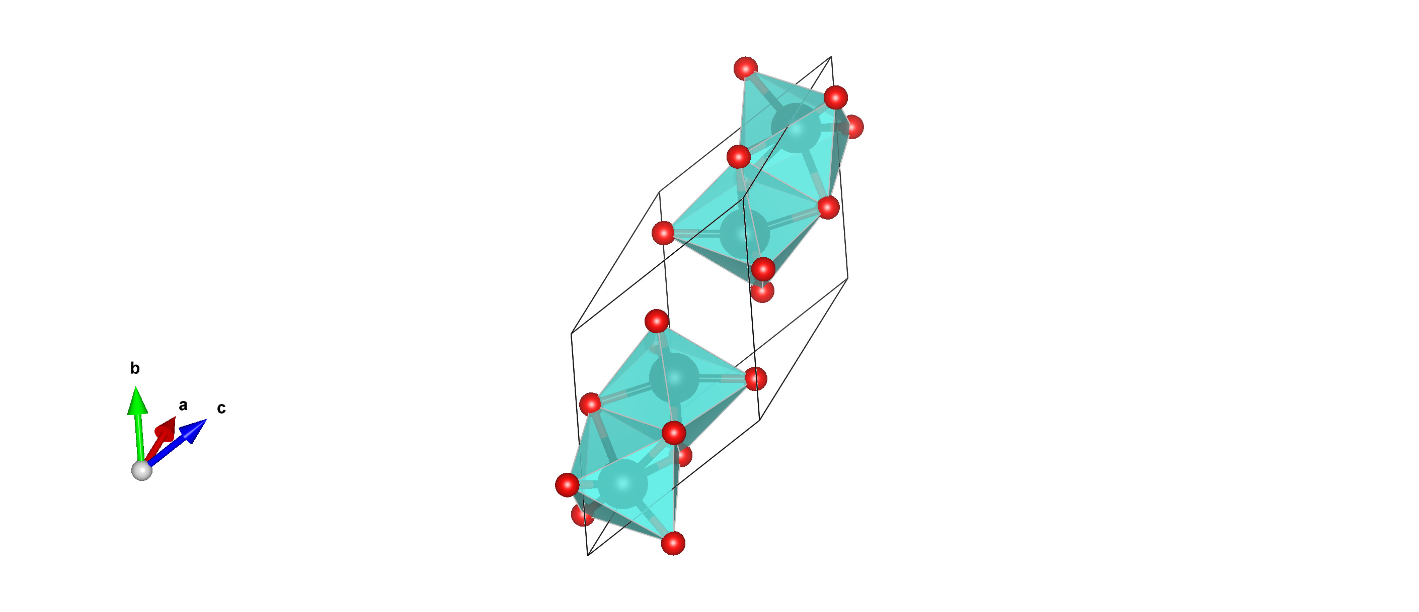
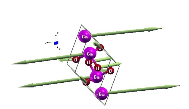
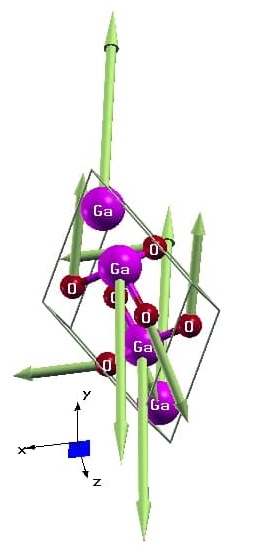
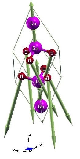
We use Quantum Espresso [16, 17], a planewave pseudopotential based DFT package for our calculation. All the calculations in the present work is done under the Local Density Approximation (LDA) for the exchange-correlation functional. In our calculations, we have used a 10 atom rhombohedral primitive cell which has 4 equivalent Ga (Gallium) atoms in distorted octahedral sites and 6 O (Oxygen) atoms as shown in the along with the first Brillouin zone generated using XCrysden [18] and Vesta [19] whereas the conventional cell has 30 atoms.
We first start with the structural relaxation after accounting for the convergence in the planewave energy cutoff and the reciprocal space grid. We have used the cutoff energy for planewave expansion of , charge density cutoff of and a centered grid of size by checking for the convergence of the total energy. We have taken the Gallium 3d orbitals as the part of the valence bands when choosing the pseudopotential. After the structural relaxation, we perform the atomic relaxation to minimize the forces on the atoms () which otherwise might give spurious results due to the structural instability during the lattice dynamics calculations. The relaxed structural parameters given in [20] are dependent on the type of the pseudopotential used during the self-consistent run.
| Lattice Parameters | |||
| a () | 4.9876 | 4.983 | |
|
13.3593 | 13.433 | |
| Fractional Coordinates | |||
| z (Ga) | 0.3565 | 0.3554 | |
| x (O) | 0.3018 | 0.3049 | |
3.2 Electronic Structure
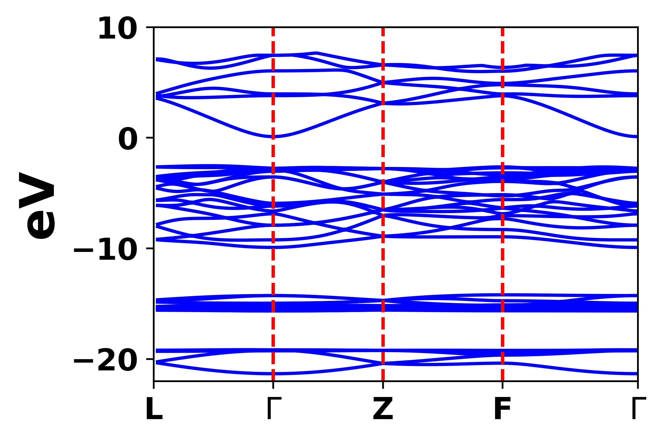
The electronic structure is calculated under the local density approximation, as such it underestimated the band gap which is a well known problem arising mainly due to the error in the self-interaction correction by the exchange-correlation functional. The bandgap problem can be overcome by use of higher order XC (exchange-correlation) functionals, and there are some results of this in the literature which estimates the indirect bandgap of and a direct bandgap of [3]. Since the low field electron transport is not impacted by the bandgap, we use LDA band structure in our calculations as shown in the . After computing the converged charge density on a coarse reciprocal space grid of size , we employ the technique of Wannier interpolation [21, 22, 23] to obtain the electronic structure on a fine grid. The idea behind the Wannier interpolation is to do a unitary rotation of the Hamiltonian from the Bloch space to the localized Wannier space and then rotating it back to the fine grid in the Bloch space. This is done using the maximally localized Wannier functions where the Hamiltonian in the Wannier space is given as:
| (1) |
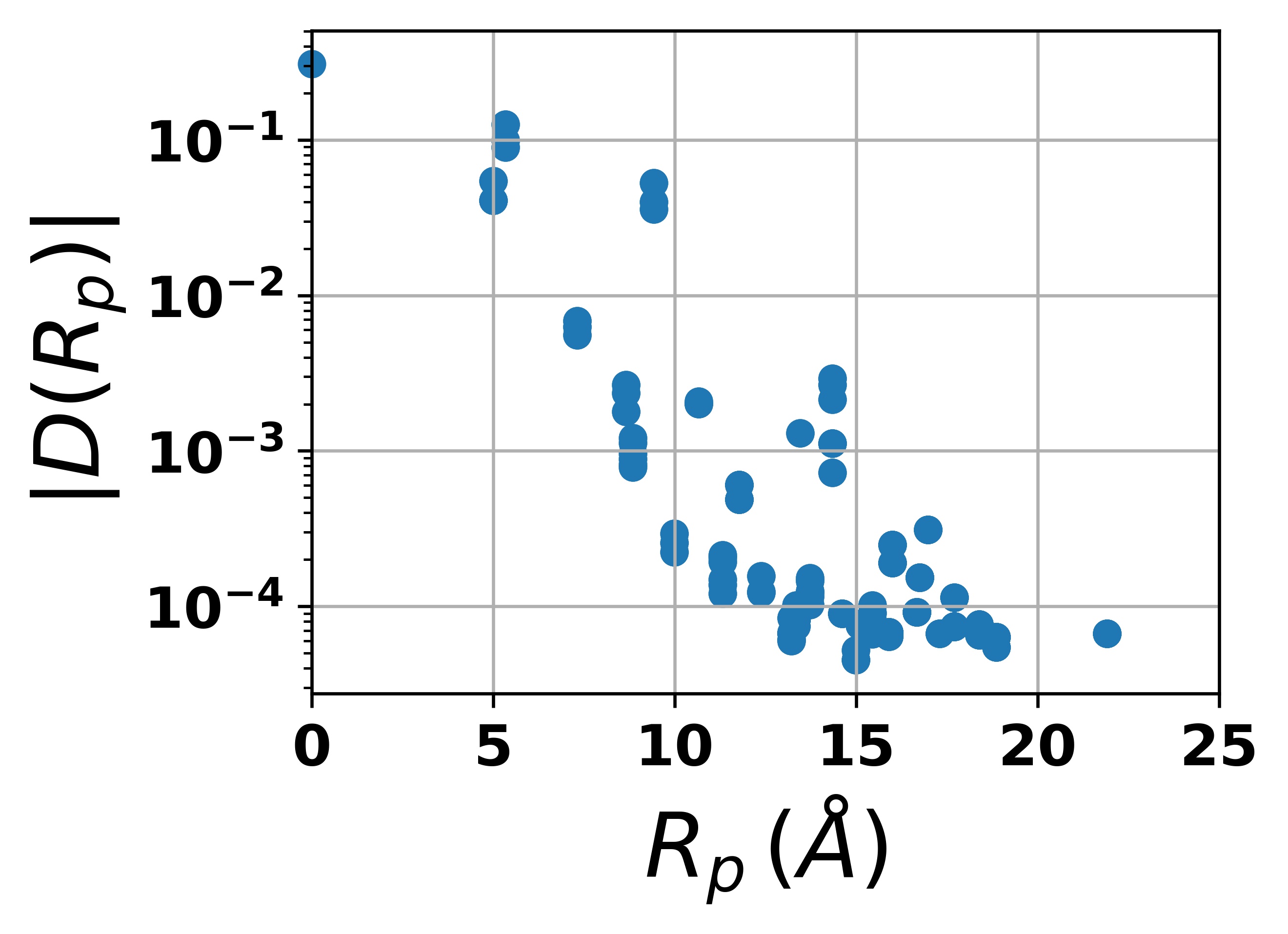
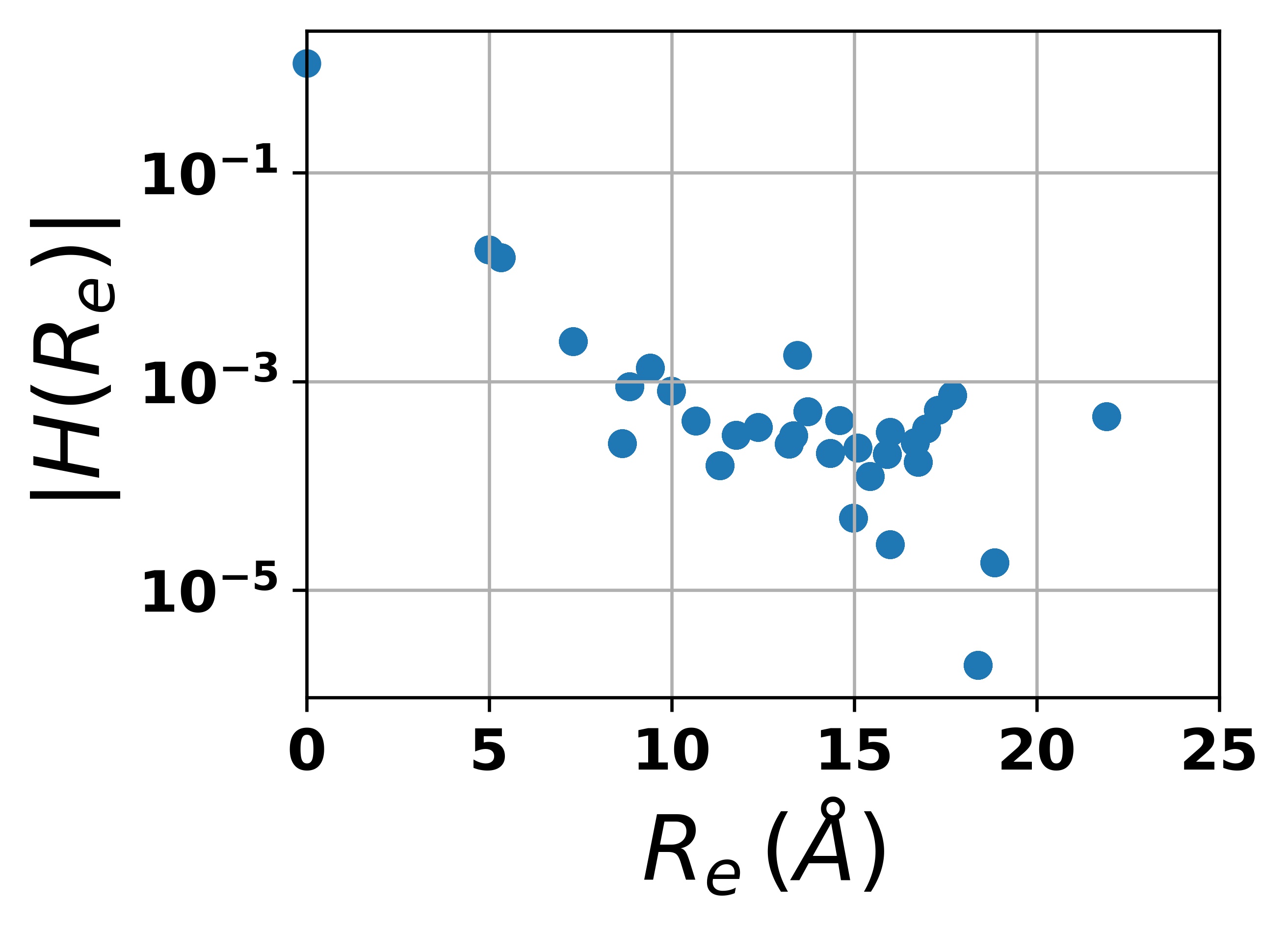
where is the electronic Hamiltonian in the coarse Bloch space, is the Wigner-Seitz cell centers and are the unitary rotation matrices for band mixing and gauge transformation. During the interpolation using Wannier functions, we also check for the spatial localization of the electronic Hamiltonian and the phonon Dynamical matrix, the plots of which are shown in and respectively. The figures clearly shown qualitatively the spatial decay of the Hamiltonian and the Dynamical matrix in the real space. The plot of the partial density of states shows that the valence band is formed by the O 2p orbitals and the conduction band by the Ga 4s orbitals, similar to that observed in . The calculated effective mass is 0.25*m0, which is comparable to the previous reported value [3]. The effective mass is slightly lower than the phase (0.3) [11], which should help in increasing the electron mobility when compared to the phase.
3.3 Lattice Dynamics
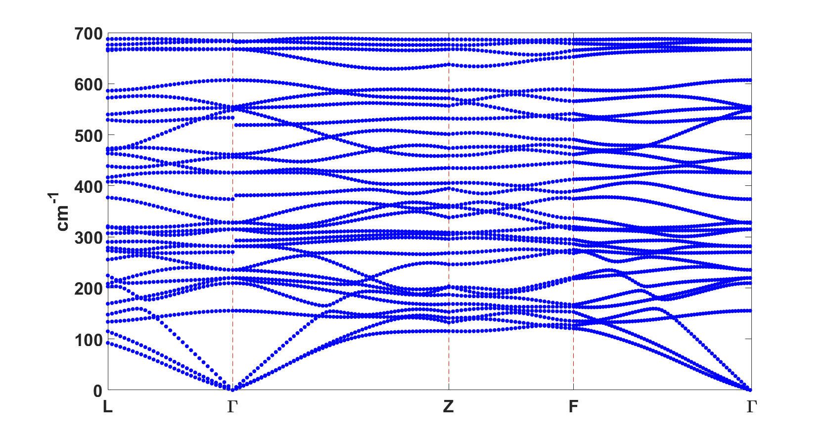
We then use the density functional perturbation theory [24], a linear response theory as implemented in the Quantum Espresso package to calculate the lattice dynamical properties. A reciprocal space phonon wavevector grid is used for this calculation to obtain the polarization vectors and the perturbation in the potential due to the atomic vibration. To calculate the phonon dispersion along the directions of the electronic structure in the irreducible wedge of the Brillouin zone, the dynamical matrix is interpolated using the Fourier interpolation technique and then diagonalized on a dense grid. The resulting phonon spectrum is shown in the . The long range correction to the dynamical matrix arising from the coupling of the macroscopic field with the LO modes, which shifts the energy of the LO mode, is taken into account by explicitly adding the non-analytical term to the dynamical matrix before diagonalization. We can see the discontinuity (circled in red) in the phonon spectrum in the at the point arising due to the split between the LO and TO modes.
The polar nature of the material results in charges on the ions which maybe more than the oxidation state of the isolated ion. It is known as Born effective charge which is a tensor quantity. It is calculated at the point along with the high frequency dielectric tensor. Both these quantities are related to the atomic polarization. The DC dielectric constant is obtained using the LST (Lyddane-Sachs-Teller) relation. As shown in , the high frequency dielectric tensor is nearly isotropic, with the space group symmetry resulting in and a small anisotropy in but the DC dielectric constant captures anisotropy arising due to the IR (infrared) mode polarization directions and the resulting direction dependent LO-TO split.
| X | Y | Z | |||
| 27.2686 | 27.2748 | 27.2686 | 27.2748 | 33.4148 | 53.9783 |
| 40.5946 | 46.3179 | 40.5946 | 46.3179 | ||
| 57.0628 | 67.7224 | 57.0628 | 67.7244 | 66.0624 | 83.6049 |
| 68.35 | 84.5809 | 68.35 | 84.5809 | ||
| = 4.62 | = 4.62 | = 4.465 | |||
| = 12.9816 | = 12.9816 | = 18.6645 | |||
There are 27 optical modes in and the symmetry reduction results in 10 IR active modes as shown in the . Of the 10 IR modes, 4 modes are doubly degenerate with the mechanical representation as . The net dipole moment of the 4(doubly degenerate) modes are polarized in the x and y cartesian directions () as shown in respectively and the remaining 2 modes are polarized in the z direction () shown in . The directional polarization is captured in the DC dielectric constant and the LO-TO split. The strength of each of the IR active modes is directly proportional to the dipole moment and is calculated as the product of the Born effective charge and the atomic displacement pattern at the Brillouin zone centre. shows the comparison between the calculated IR active frequencies and the experimentally observed frequencies [25], showing a close match.
| IR Modes () | |
|---|---|
| 220.88 | Not Observed |
| 328.82 | 333.4 |
| 462.21 | 469.9 |
| 553.64 | 562.7 |
| 270.66 | 280 |
| 535.11 | 544 |
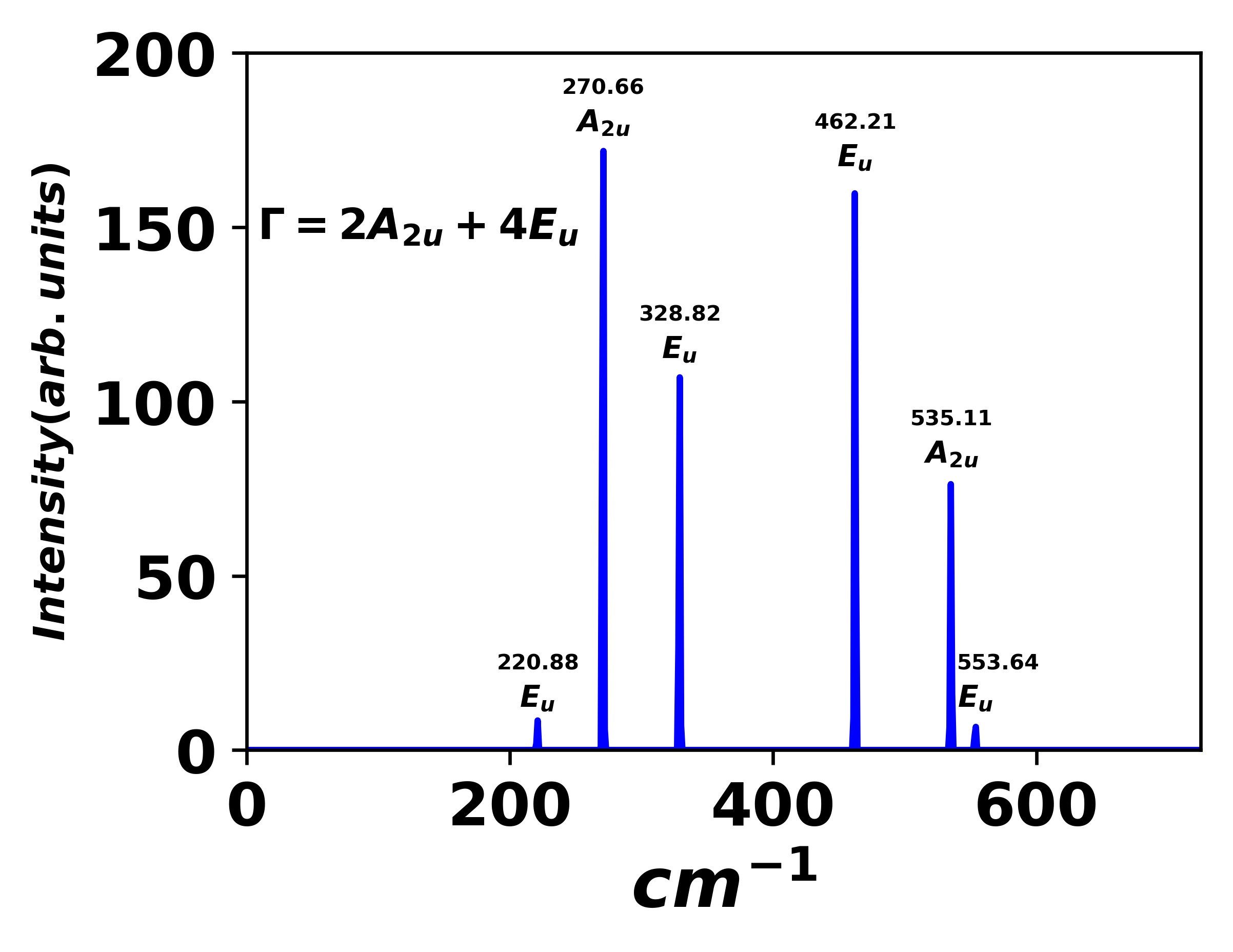
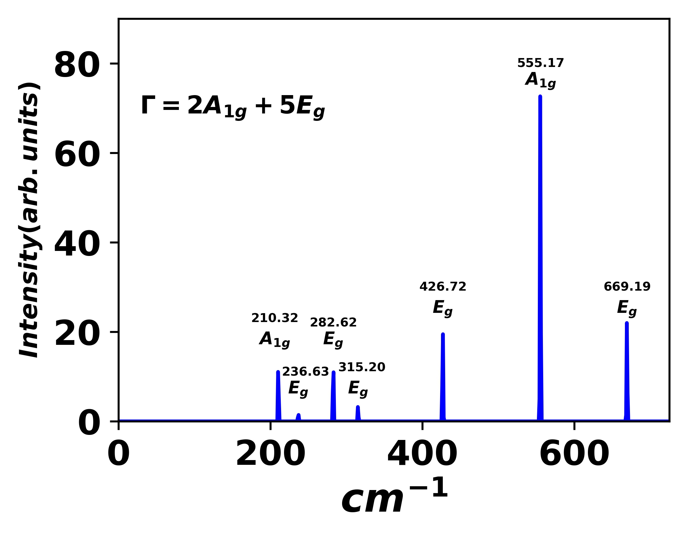
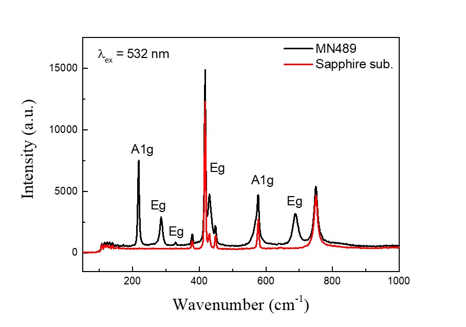
There are 12 Raman active modes in where 5 modes are doubly degenerate represented as . The non-resonant Raman coefficients are calculated under the formalism proposed by Lazzeri et.al [26] and is implemented in the Quantum Espresso package. The calculated Raman spectra closely matches the spectra contained experimentally[27] as shown in the . The slight shift in the theoretical values compared to the experimental results may arise due to the dependence of the structural parameters on the pseudopotential used in the self-consistent calculation. compares the theoretical Raman frequencies with the experimental observations.
| Raman Modes () | ||
| 236.63 | 240.7 | Not Observed |
| 282.62 | 285.3 | 286 |
| 315.2 | 328.8 | 328 |
| 426.72 | 430.7 | 431 |
| 669.19 | 686.7 | 688 |
| 210.32 | 218.2 | 218 |
| 555.17 | 569.7 | 576 |
4 Scattering Rates
The scattering rate is proportional to square of the EPI () interaction elements which are calculated from the perturbation in the potential due to the lattice motion. The elements are the strength of transition from one state to another and are calculated by taking the overlap of the wavefunctions of the initial and final state in the presence of a perturbing potential. The generalized EPI element is given as:
| (2) |
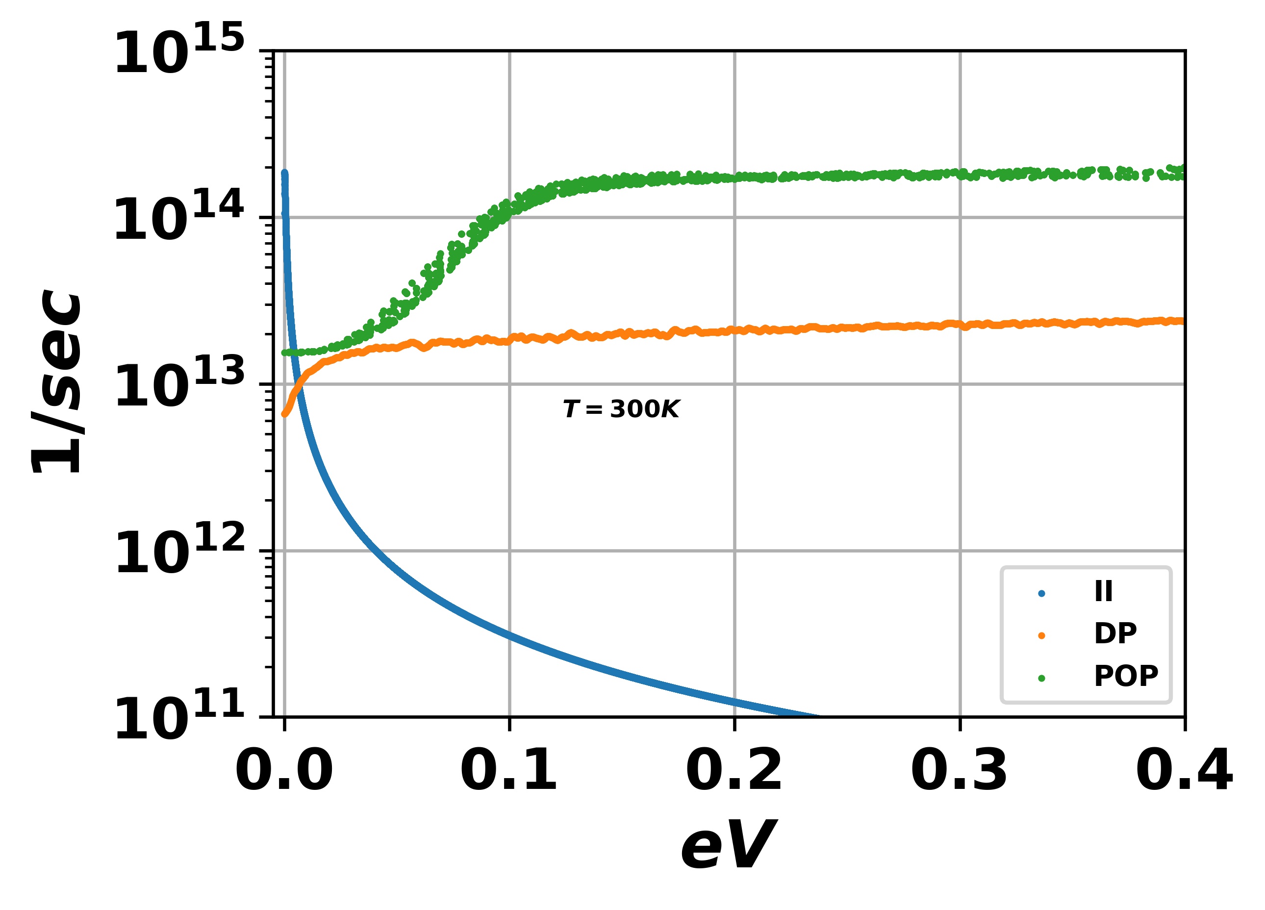
where is electronic wavefunction and is the perturbed potential due to lattice motion. We calculate the scattering rate using the Fermi’s Golden rule. The q space integration in the Fermi’s golden rule is carried out using the technique of Gaussian smearing for the energy conservation function. In the present calculation, we have used the parabolic band approximation with an isotropic effective mass. The shows the polar optical phonon scattering, the non-polar scattering and the ionized impurity scattering rate calculated at 300K. We have taken the donor density of with donor activation energy of [11] assuming Silicon as the donor material.
4.1 Polar Optical Phonon Scattering
To calculate the polar optical phonon EPI elements, we use the Vogl model [28] under two different schemes. The Frohlich model that is widely used to estimate the EPI elements has a major drawback; it does not consider the anisotropy in the dipole moment and assumes the LO modes to be dispersion less. The Frohlich interaction elements are given by:
| (3) |
where is the phonon frequency of a given mode at the point, is the normalization volume, is the spatially averaged high frequency dielectric constant and is the static dielectric constant. From the equation, it is clear that taking the spatial average of the dielectric constant leads to the averaging of the anisotropic effects and also it does not take into consideration the polarization direction of each mode of the phonon spectrum.
To incorporate the anisotropy in the EPI elements, we use the Vogl model. In the first scheme, we still assume the phonon spectrum to be dispersion less, but we take the projection of the dipole moment for each mode onto the phonon wavevector thus accounting for the anisotropic LO-TO split. The expression for the EPI elements used under this scheme is given by [29]:
| (4) |
where, is the Born effective charge, is the phonon eigenvector for each atom in the unit cell at the point, is the phonon frequency of each mode, is the atomic mass of each of the constituent atoms and is the Thomas-Fermi screening wavevector. The inclusion of the screening term circumvents the divergence at [29]. The high frequency dielectric constant is nearly spatially isotropic; hence we take the average of the trace of the dielectric tensor. The screening wavevector is calculated from the Fermi energy and is expressed as:
| (5) |
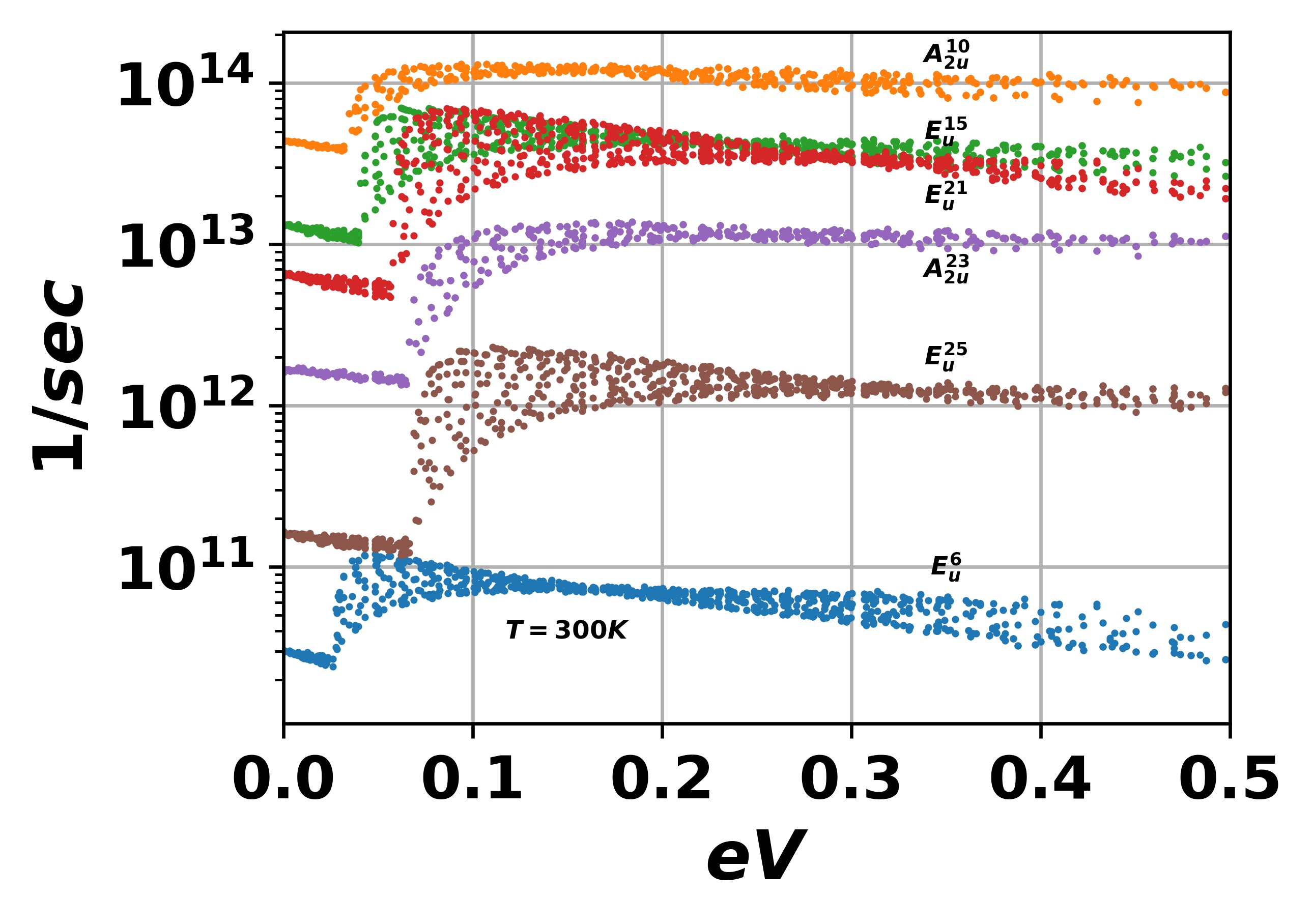
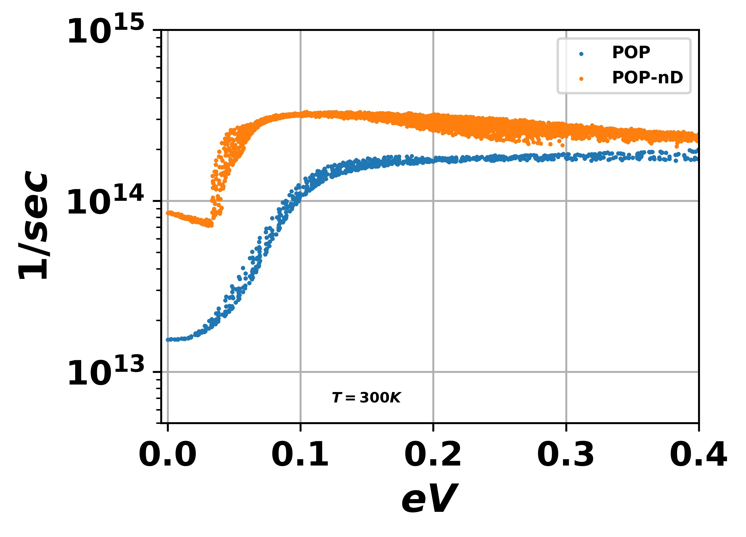
where, is the Fermi energy and is the charge density. One of the drawbacks of this assumption is the approximation of the dispersion less phonon spectrum. This approximation overestimates the scattering rate when compared to the full phonon dispersion, as can be seen in the . The net strength of the dipole moment decreases moving away from the point and hence the contribution from the point to the scattering rate also decreases. However, this is not the case when we assume dispersion less phonon spectrum. The EPI elements in this case only decay because of the increase in the magnitude of the phonon wavevector as the dipole moment remains constant. From the plot of the IR spectrum in , we see that the (270.66 ) mode has the maximum IR strength and hence is expected to contribute most to the scattering rate. Moreover, the phonon occupancy of this mode (270.66 ) is high at room temperature which will again play a major role in determining the dominant scattering mode. The mode dependent plot of the bulk scattering rate in clearly shows the dominant mode. Also, from the figure, we can see sharp emissions depicted by the sudden change in slope, depending on the energy of each mode. Another noteworthy point is that the degenerate energy levels have different scattering rates arising due to the anisotropy which is averaged out when calculating the electron mobility.
In the second scheme, we consider the full phonon dispersion, but we do not explicitly include any screening. We only use the high frequency dielectric constant tensor to screen the LO phonons arising due to the valence electrons. The generalized expression for the Vogl model for the polar optical phonon EPI elements proposed by Carla Verdi et.al[30] is given as:
|
|
(6) |
where, is the atomic position, is the phonon frequency and are the unitary rotation matrices. The sum is over all the reciprocal lattice vectors G and the number of atoms in the unit cell. WE have used 64000 k points and 68921 q points for the EPI calculation. The product of matrices accounts for the overlap of the wavefunction and can be obtained during the Wannier interpolation. The polar optical phonon scattering rate is shown in the .
4.2 Non Polar Scattering
The non polar EPI elements are calculated using the EPW code [31]. The total electron phonon interaction elements calculated using , is split into the longrange and the shortrange component for interpolation from coarse grid onto a fine grid using the Wannier functions. The longrange part of the EPI elements cannot be interpolated using the Wannier functions because of the localized nature of the Wannier functions in the real space.
The shortrange elements consist of deformation potential scattering elements (both optical and acoustic). Once the shortrange EPI elements are calculated on a coarse grid, the interpolation on to a fine grid is done in two steps: firstly, the EPI elements in the Wannier space is interpolated onto a fine reciprocal space phonon wavevector grid i.e phonon Bloch representation. The resulting interaction elements are now in the electronic Wannier space and fine phonon Bloch space. We extract the EPI’s at this stage and then use the Fourier interpolation to calculate the elements on a fine electronic Bloch space given as [32]:
| (7) |
where are the EPI elements on a fine electron and phonon reciprocal space grid, is the degeneracy of the Wigner-Seitz cell, is the Wigner-Seitz cell center, is the EPI elements on a fine phonon grid in Bloch space and electronic Wannier space. The unitary rotation matrices are unity in our case, since the number of bands inside the energy window used during the process of Wannierization [22, 23] is just one i.e the lowermost conduction band. Such band mixing is done to remove non-analyticity in the bands which may arise due to the band crossing making the maximal localization of the Wannier functions challenging.
To calculate the scattering rate, we use the Fermi’s Golden rule, by interpolating the EPI elements on a fine k and q point grid on the fly and using Gaussian smearing for energy conservation. For the shortrange scattering rate calculation, we have used around 45000 q points and 55000 k points distributed uniformly inside the Brillouin zone. We have covered only of the Brillouin zone, because large phonon wavevectors will not contribute to the scattering process due to the unavailability of equivalent valleys to account for such a large momentum change.
4.3 Ionized Impurity Scattering
The ionized impurity scattering rate is calculated using the Brooks Herring model [33] with a constant Debye like screening. The analytic expression for the momentum relaxation time for the ionized impurity scattering is given by [34]:
| (8) |
where is the function of the Debye length, is the DC dielectric constant, is the electron momentum and is the total impurity concentration. In we can see that at very low energies, the ionized impurity scattering is the dominant mechanism and it falls off rapidly with the increase in the electron energy since the duration of interaction of the screened field with the electron decreases. We have used the spatially averaged DC dielectric constant, thus loosing information about anisotropy that arises due to the LO-TO split as is evident from .
5 Electron Mobility
In this study, we use the relaxation time approximation to calculate the electron mobility which is given by:
| (9) |
where, is the electron mobility in , is the electronic charge, is the electron effective mass and is the average relaxation time. The average value is calculated as [35]:
| (10) |
where, is the equilibrium Fermi-Dirac distribution, is the electron energy and is the relaxation time. We calculate the mobility for all the three different scattering mechanism we have accounted for and then use the Matthiessen’s rule to calculate the overall electron mobility which is given as:
| (11) |
where, , and is the mobility due to the polar optical phonon, non-polar and ionized impurity scattering respectively. We do this calculation at and the bulk electron mobility obtained is about . This is dominated by the POP ()and non-polar phonon () as compared to the ionized impurity scattering. These calcualted values are just the first order approximation to the electron mobility. Using better approximation to solve the Boltzmann transport equation would be through the Rode’s iterative technique can increase the mobility by around . Also the inclusion of screening will result in the further increase of electron mobility.
6 Conclusion
We have theoretically investigated the electron-phonon coupling in and estimated the low field electron mobility at 300K. We take into account the polar optical phonon, ionized impurity and deformation potential scattering for the mobility calculation. The polar optical phonon interaction elements were estimated assuming dispersion less phonon spectrum and also with the full phonon dispersion. The DC dielectric constant was calculated using LST relation which clearly shows strong anisotropy in the z cartesian direction. The infrared and the Raman spectrum was calculated and compared with the experiments showing close match.
7 Acknowledgement
We acknowledge the support from Air Force Office of Scientific Research under award number FA9550-18-1-0479 (Program Manager: Ali Sayir) and from NSF under awards ECCS 1607833 and ECCS - 1809077. We also acknowledge the high-performance computing cluster provided by The Centre for Computational Research at the University at Buffalo.
References
- [1] Rustum Roy, V. G. Hill, and E. F. Osborn. Polymorphism of and the system . Journal of the American Chemical Society, 74(3):719–722, 1952.
- [2] H. Y. Playford, A. C. Hannon, E. R. Barney, and R. I. Walton. Structures of uncharacterised polymorphs of gallium oxide from total neutron diffraction. Chemistry, 19(8):2803–2813, Feb 2013.
- [3] Haiying He, Roberto Orlando, Miguel A. Blanco, Ravindra Pandey, Emilie Amzallag, Isabelle Baraille, and Michel Rérat. First-principles study of the structural, electronic, and optical properties of in its monoclinic and hexagonal phases. Phys. Rev. B, 74:195123, Nov 2006.
- [4] Masataka Higashiwaki, Kohei Sasaki, Akito Kuramata, Takekazu Masui, and Shigenobu Yamakoshi. Development of gallium oxide power devices. physica status solidi (a), 211(1):21–26, 2014.
- [5] Masataka Higashiwaki, Kohei Sasaki, Hisashi Murakami, Yoshinao Kumagai, Akinori Koukitu, Akito Kuramata, Takekazu Masui, and Shigenobu Yamakoshi. Recent progress in power devices. Semiconductor Science and Technology, 31(3):034001, jan 2016.
- [6] K. Zeng, A. Vaidya, and U. Singisetti. 1.85 kv breakdown voltage in lateral field-plated mosfets. IEEE Electron Device Letters, 39(9):1385–1388, Sep. 2018.
- [7] K. Sasaki, M. Higashiwaki, A. Kuramata, T. Masui, and S. Yamakoshi. schottky barrier diodes fabricated by using single-crystal – (010) substrates. IEEE Electron Device Letters, 34(4):493–495, April 2013.
- [8] Toshiyuki Oishi, Yuta Koga, Kazuya Harada, and Makoto Kasu. High-mobility single crystals grown by edge-defined film-fed growth method and their schottky barrier diodes with contact. Applied Physics Express, 8(3):031101, feb 2015.
- [9] M. H. Wong, K. Goto, H. Murakami, Y. Kumagai, and M. Higashiwaki. Current aperture vertical mosfets fabricated by - and -ion implantation doping. IEEE Electron Device Letters, 40(3):431–434, March 2019.
- [10] Yi Lu, H. H. Yao, Jingtao Li, Jianchang Yan, Junxi Wang, Jinmin Li, and Xiaohang Li. Aln/beta-ga2o3 based hemt: a potential pathway to ultimate high power device. 2019.
- [11] Krishnendu Ghosh and Uttam Singisetti. Ab initio calculation of electron–phonon coupling in monoclinic crystal. Applied Physics Letters, 109(7):072102, 2016.
- [12] J.W. Roberts, P.R. Chalker, B. Ding, R.A. Oliver, J.T. Gibbon, L.A.H. Jones, V.R. Dhanak, L.J. Phillips, J.D. Major, and F.C.-P. Massabuau. Low temperature growth and optical properties of deposited on sapphire by plasma enhanced atomic layer deposition. Journal of Crystal Growth, 528:125254, 2019.
- [13] J. H. Leach, K. Udwary, J. Rumsey, G. Dodson, H. Splawn, and K. R. Evans. Halide vapor phase epitaxial growth of and films. APL Materials, 7(2):022504, 2019.
- [14] Daisuke Shinohara and Shizuo Fujita. Heteroepitaxy of corundum-structured thin films on substrates by ultrasonic mist chemical vapor deposition. Japanese Journal of Applied Physics, 47(9):7311–7313, Sep 2008.
- [15] Krishnendu Ghosh and Uttam Singisetti. Theory of high field transport in . International Journal of High Speed Electronics and Systems, 28(01n02):1940008, 2019.
- [16] P Giannozzi, O Andreussi, T Brumme, O Bunau, M Buongiorno Nardelli, M Calandra, R Car, C Cavazzoni, D Ceresoli, M Cococcioni, N Colonna, I Carnimeo, A Dal Corso, S de Gironcoli, P Delugas, R A DiStasio Jr, A Ferretti, A Floris, G Fratesi, G Fugallo, R Gebauer, U Gerstmann, F Giustino, T Gorni, J Jia, M Kawamura, H-Y Ko, A Kokalj, E Küçükbenli, M Lazzeri, M Marsili, N Marzari, F Mauri, N L Nguyen, H-V Nguyen, A Otero de-la Roza, L Paulatto, S Poncé, D Rocca, R Sabatini, B Santra, M Schlipf, A P Seitsonen, A Smogunov, I Timrov, T Thonhauser, P Umari, N Vast, X Wu, and S Baroni. Advanced capabilities for materials modelling with quantum espresso. Journal of Physics: Condensed Matter, 29(46):465901, 2017.
- [17] Paolo Giannozzi, Stefano Baroni, Nicola Bonini, Matteo Calandra, Roberto Car, Carlo Cavazzoni, Davide Ceresoli, Guido L Chiarotti, Matteo Cococcioni, Ismaila Dabo, Andrea Dal Corso, Stefano de Gironcoli, Stefano Fabris, Guido Fratesi, Ralph Gebauer, Uwe Gerstmann, Christos Gougoussis, Anton Kokalj, Michele Lazzeri, Layla Martin-Samos, Nicola Marzari, Francesco Mauri, Riccardo Mazzarello, Stefano Paolini, Alfredo Pasquarello, Lorenzo Paulatto, Carlo Sbraccia, Sandro Scandolo, Gabriele Sclauzero, Ari P Seitsonen, Alexander Smogunov, Paolo Umari, and Renata M Wentzcovitch. Quantum espresso: a modular and open-source software project for quantum simulations of materials. Journal of Physics: Condensed Matter, 21(39):395502 (19pp), 2009.
- [18] Anton Kokalj. Xcrysden—a new program for displaying crystalline structures and electron densities. Journal of Molecular Graphics and Modelling, 17(3):176 – 179, 1999.
- [19] Koichi Momma and Fujio Izumi. VESTA3 for three-dimensional visualization of crystal, volumetric and morphology data. Journal of Applied Crystallography, 44(6):1272–1276, Dec 2011.
- [20] M. Marezio and J. P. Remeika. Bond lengths in the structure and the high-pressure phase of . The Journal of Chemical Physics, 46(5):1862–1865, 1967.
- [21] Gregory H. Wannier. The structure of electronic excitation levels in insulating crystals. Phys. Rev., 52:191–197, Aug 1937.
- [22] Nicola Marzari and David Vanderbilt. Maximally localized generalized wannier functions for composite energy bands. Phys. Rev. B, 56:12847–12865, Nov 1997.
- [23] Nicola Marzari, Arash A. Mostofi, Jonathan R. Yates, Ivo Souza, and David Vanderbilt. Maximally localized wannier functions: Theory and applications. Rev. Mod. Phys., 84:1419–1475, Oct 2012.
- [24] Xavier Gonze and Changyol Lee. Dynamical matrices, born effective charges, dielectric permittivity tensors, and interatomic force constants from density-functional perturbation theory. Phys. Rev. B, 55:10355–10368, Apr 1997.
- [25] Martin Feneberg, Jakob Nixdorf, Maciej D. Neumann, Norbert Esser, Lluis Artús, Ramon Cuscó, Tomohiro Yamaguchi, and Rüdiger Goldhahn. Ordinary dielectric function of corundumlike from 40 mev to 20 ev. Phys. Rev. Materials, 2:044601, Apr 2018.
- [26] Michele Lazzeri and Francesco Mauri. First-principles calculation of vibrational raman spectra in large systems: Signature of small rings in crystalline . Phys. Rev. Lett., 90:036401, Jan 2003.
- [27] R. Cuscó, N. Domènech-Amador, T. Hatakeyama, T. Yamaguchi, T. Honda, and L. Artús. Lattice dynamics of a mist-chemical vapor deposition-grown corundum-like single crystal. Journal of Applied Physics, 117(18):185706, 2015.
- [28] P. Vogl. Microscopic theory of electron-phonon interaction in insulators or semiconductors. Phys. Rev. B, 13:694–704, Jan 1976.
- [29] Youngho Kang, Karthik Krishnaswamy, Hartwin Peelaers, and Chris G Van de Walle. Fundamental limits on the electron mobility of . Journal of Physics: Condensed Matter, 29(23):234001, May 2017.
- [30] Carla Verdi and Feliciano Giustino. Frohlich electron-phonon vertex from first principles. Phys. Rev. Lett., 115:176401, Oct 2015.
- [31] S. Poncé, E.R. Margine, C. Verdi, and F. Giustino. Epw: Electron–phonon coupling, transport and superconducting properties using maximally localized wannier functions. Computer Physics Communications, 209:116 – 133, 2016.
- [32] Feliciano Giustino, Marvin L. Cohen, and Steven G. Louie. Electron-phonon interaction using wannier functions. Phys. Rev. B, 76:165108, Oct 2007.
- [33] D. Chattopadhyay and H. J. Queisser. Electron scattering by ionized impurities in semiconductors. Rev. Mod. Phys., 53:745–768, Oct 1981.
- [34] Mark Lundstrom. Fundamentals of Carrier Transport. Cambridge University Press, 2 edition, 2000.
- [35] Antonella Parisini and Roberto Fornari. Analysis of the scattering mechanisms controlling electron mobility in crystals. Semiconductor Science and Technology, 31(3):035023, Feb 2016.