Compound Guided Waves That Mix Characteristics of Surface-Plasmon-Polariton,
Tamm, Dyakonov–Tamm, and Uller–Zenneck Waves
Francesco Chiadini,1 Vincenzo Fiumara,2 Antonio Scaglione,1 and Akhlesh Lakhtakia3
1Department of Industrial Engineering, University of Salerno, via Giovanni Paolo II,
132 - Fisciano (SA), 84084, Italy
2School of Engineering, University of Basilicata, Viale dell’Ateneo Lucano 10, 85100 Potenza, Italy
3Department of Engineering Science and Mechanics, Pennsylvania State University,
University Park, PA 16802–6812, USA
Abstract.
Solutions of the boundary-value problem for electromagnetic waves guided by a layer of a homogeneous and isotropic (metal or dielectric) material sandwiched between a structurally chiral material (SCM) and a periodically multi-layered isotropic dielectric (PMLID) material were numerically obtained and analyzed. If the sandwiched layer is sufficiently thick, the two bimaterial interfaces decouple from each other, and each interface may guide one or more electromagnetic surface waves (ESWs) by itself. Depending on the constitution of the two materials that partner to form an interface, the ESWs can be classified as surface-plasmon-polarition (SPP) waves, Tamm waves, Dyakonov–Tamm waves, or Uller–Zenneck waves. When the sandwiched layer is sufficiently thin, the ESWs for single bimaterial interfaces coalesce to form compound guided waves (CGWs). The phase speeds, propagation distances, and spatial profiles of the electromagnetic fields of CGWs are different from those of the ESWs. The energy of a CGW is distributed in both the SCM and the PMLID material, if the sandwiched layer is sufficiently thin. Some CGWs require the sandwiched layer to have a minimum thickness. Indeed, the coupling between the two faces of the sandwiched layer is affected by the ratio of the thickness of the sandwiched layer to the skin depth in that material and the rates at which the fields of the ESWs guided individually by the two interfaces decay away from their respective guiding interfaces.
1 Introduction
Several different kinds of electromagnetic surface waves (ESWs) exist. Perhaps the first ever analytical treatment was of an ESW guided by the planar interface of air and seawater, published in his doctoral dissertation by Uller in 1903 [1]. As Wait [2] recounted in a review of ground-wave propagation, that was also the time when Tesla [3] conjectured that radio waves are guided by the air/earth interface, a proposition analyzed by Zenneck [4] in 1907 and by Sommerfeld [5, 6, 7] in several papers thereafter. The ESWs bound to the planar interface of two homogeneous dielectric materials of which one is dissipative are called Zenneck waves, but should be more properly called Uller–Zenneck waves [8].
ESWs called surface-plasmon-polariton (SPP) waves are guided by the planar interface of two isotropic and homogeneous materials, one of which has a relative permittivity with negative real part (usually, a metal) and the other whose relative permittivity has positive real part (usually, a dielectric material). SPP waves became a topic of research after the energy losses of electrons impinging on a metal film were explained in 1957 in terms of electronic-plasma oscillations occurring at the film’s surfaces [9]. But SPP waves cannot be excited by shining light directly at either a dielectric film lying atop a metal film or a metal film lying atop a dielectric film. The reflectance of a parallel-polarized plane wave from a thin aluminum film deposited on the hypotenuse of a right-angled glass prism was shown in 1959 to exhibit a sharp dip as the angle of incidence exceeded the critical angle for a planar glass/air interface [10]. The reflectance dip was related to the excitation of an SPP wave in 1968 [11, 12], and an explosive expansion of research on applications of SPP waves started thereafter [13, 14, 15]. The excitation of a multiplicity of SPP waves at a specific frequency is possible if the dielectric partnering material is periodically non-homogeneous (on the order of wavelength) in the direction normal to the interface [16, 17]. In this case, even though all SPP waves are excited at the same frequency, they can differ for polarization state, phase speed, attenuation rate, and field profile; furthermore, the dielectric partnering material can even be anisotropic [18, 16].
Most SPP waves do not propagate long distances along the interface plane, because metals are dissipative. If both partnering materials are weakly dissipative dielectric materials, the propagation distance would be enhanced. Indeed, the Tamm wave was predicted in 1977 to be guided by the interface of two isotropic dielectric materials, at least one of which was periodically non-homogeneous in the direction perpendicular to the interface [19]. The experimental observation of Tamm waves followed in 1978 [20], and their application to optical sensing has been subsequently demonstrated [21, 22].
A few years later, Marchevskiĭ et al. [23] and Dyakonov [24] predicted an ESW guided by the interface of two homogeneous dielectric materials, at least one of which is anisotropic. Experimental verification came only in 2009, when Takayama et al. were able to excite a Dyakonov wave guided by the interface of a liquid and a biaxial dielectric crystal [25]. But the Dyakonov wave propagates in very narrow ranges of directions ( deg out of a maximum of deg) in the interface plane [26], and is difficult to detect. The insertion of a 10–20-nm thick dielectric sheet between an anisotropic and an isotropic material can enhance the range of directions of propagation [27].
In 2007 Lakhtakia and Polo [28] proposed an ESW that is guided by the interface of two dielectric materials, one of which is isotropic and homogeneous, and the other is both anisotropic and periodically non-homogeneous in the direction perpendicular to the interface plane. Combining the attributes of both Tamm and Dyakonov waves, this surface wave was named a Dyakonov–Tamm wave. The angular sectors permitting the propagation of Dyakonov–Tamm waves are so large as to often cover the entire 360 deg available [16]. Dyakonov–Tamm waves are also expected to be useful for optical sensing [29].
Two SPP waves can be compounded when a metal layer of thickness is sandwiched between two half spaces filled with isotropic, homogeneous dielectric materials [30, 31, 32]. But must not be significantly larger than the skin depth in the metal, or the coupling between the two dielectric/metal interfaces vanishes and each of the two interfaces by itself guides an SPP wave that will not coalesce with the other SPP wave. The compound guided wave (CGW) can propagate over longer distances than an SPP wave guided by a single metal/dielectric interface. Recently, we examined the CGWs guided by a thin metal layer sandwiched between a homogeneous isotropic dielectric (HID) material and either a periodically multi-layered isotropic dielectric (PMLID) material [33] or a structurally chiral material (SCM) [34], all dielectric non-metallic materials being assumed to have negligible dissipation. We found that a multiplicity of CGWs with plasmonic and polaritonic constituents can propagate bound to both metal/dielectric interfaces with energy distributed in both the dielectric materials if the metal layer is sufficiently thin. Long-range CGWs are also guided by a thin metal layer inserted in a periodically non-homogeneous anisotropic material such that the direction of non-homogeneity is the same as the thickness direction of the metal film [35] with non-homogeneity on the wavelength scale; furthermore, CGWs resembling Dyakonov–Tamm waves in their characteristics are guided, if the sandwiched metal is replaced by an isotropic dielectric material [36]. Finally, CGWs that fuse together the characteristics of SPP waves and Dyakonov waves have been theoretically shown to excited via a uniaxial dielectric layer inserted between a HID material and a metal [37]. Thus, planar multi-interface structures offer the possibility of CGWs that mix the characteristics of two (or more) ESWs.
With our interest lying in the compounding of ESWs that require at least one of the partnering materials to be periodically non-homogeneous normal to the direction of propagation, in the present paper, we address and solve the boundary-value problem of the propagation of a CGW guided by a layer of a homogeneous and isotropic (metal or dielectric) material sandwiched between an SCM and a PMLID material. Thereby, compounding of the characteristics of SPP waves, Tamm waves, Dyakonov–Tamm waves, and Uller–Zenneck waves is investigated. Let us note that the analyzed structures can be manufactured using techniques routinely used to fabricate optical thin films, especially multilayer thin films [38, 39] and sculptured thin films [40], and liquid crystals [41].
The plan of this paper is as follows: Sec. 2 provides in brief the boundary-value problem for CGWs guided by a planar A/B/C structure and introduces the materials chosen as A, B, and C for the numerical results presented in Secs. 3 and 4. Section 3 provides some results for ESWs guided by the A/B, B/C, and A/C bimaterial interfaces individually. Section 4 is devoted to numerical results for CGWs guided by the A/B/C structure and comparison with the results presented in Sec. 3. Concluding remarks follow in Sec. 5.
An dependence on time is implicit, with denoting the angular frequency and . The free-space wavenumber, the free-space wavelength, and the intrinsic impedance of free space are denoted by , , and , respectively, with and being the permeability and permittivity of free space. The speed of light in vacuum is denoted by . Vectors are in boldface; dyadics are underlined twice; and Cartesian unit vectors are identified as , , and .
2 Theoretical Preliminaries and Materials
A schematic of the boundary-value problem for the propagation of a CGW is provided in Figure 1. A slab of material B is interposed between the half space occupied by material A and the half space occupied by a material C. Given the wide variety of compound CGWs possible, we chose A to be a PMLID material, B to be a homogeneous and isotropic material, and C to be an SCM.
The PMLID material A has a period nm with a unit cell consisting of equal-thickness nondissipative dielectric layers of different silicon oxynitrides, each fabricated by plasma-enhanced chemical vapor deposition of a specific composition of silane, ammonia, and nitrous oxide [42]. The layers contain SiO2 and SiNx in the ratios shown in Table 1. The layer labeled in the first unit cell of the PMLID material is the one closest to material B.
| SiO | SiN | ||
|---|---|---|---|
For all calculations reported here, material B can be either (i) a metal, specifically silver with relative permittivity ; or (ii) a dissipative HID with which was used as a nonplasmonic analog of silver; or (iii) a practically nondissipative HID, specifically a glass with relative permittivity .
Material C was chosen to be an SCM—specifically, a structurally right-handed chiral sculptured thin film of patinal titanium oxide with permittivity dyadic given at nm by [34, 43]
| (1) | ||||
with
| (2) | |||
| (3) |
and nm as the period along the axis.
We consider the CGW to be propagating parallel to the unit vector , , in the plane and decaying far away from the layer of material B. With as the complex-valued wavenumber of the CGW, the electric and magnetic field phasors can be represented everywhere by
| (4) |

The axial field components and of and , respectively, can be expressed in terms of the column 4-vector [16]
| (5) |
that satisfies the matrix differential equations
| (6) |
where the matrixes can be written for materials A, B, and C. Since material B is homogeneous, the matrix is independent of , and we obtain
| (7) |
after solving (6) [16]. By virtue of the periodicity of both materials A, and C along the axis, we have
| (8) | |||||
| (9) |
where each of the matrixes and characterizes the optical response of one period. Whereas can be calculated as the cascade of the transfer matrixes of the layers constituting one period of the PMLID material, can be obtained by a piecewise uniform approximation subdividing one period of the SCM in thin slices, parallel to the plane , with equal thickness and spatially uniform dielectric properties [16, 40].
After the imposition of the standard boundary conditions across the interfaces and , Eqs. (7)–(9) lead to the matrix equation
| (10) |
The matrix is synthesized from the as well as from the eigenvectors of and , as shown in detail elsewhere [16, Sec. 3.6]. The column 4-vector containins 4 unknown coefficients.
Equation (10) has a nontrivial solution only when the matrix is singular. Therefore the dispersion equation has to be solved for .
We numerically solved the dispersion equation to obtain the normalized wavenumbers of the CGWs. Knowing , we can calculate the phase speed and the propagation distance of the CGW in the direction parallel to , where is the distance along the direction of propagation at which the wave amplitude reduces by a factor of and the power density reduces by . The main characteristics of the CGW can be illustrated by the spatial distribution of the time-averaged Poynting vector
| (11) |
where the asterisk denotes the complex conjugate. If both materials A and C are isotropic, the CGW is either or polarized, and as well as are independent of (i.e., the direction of propagation in the plane). But, if at least one of those two materials is an SCM, then no polarization state can be assigned to the CGW [16].
We focused on CGWs that fuse together at least two ESWs of the following kinds: SPP waves, Tamm waves, Dyakonov–Tamm waves, and Uller–Zenneck waves. In order to present representative numerical results, we fixed nm and deg, the dependence on of these CGWs being quite weak for the chosen SCM. All calculations were restricted to to avoid computational instabilities that emerged for .
3 ESWs guided by an A/B, B/C, or A/C bimaterial interface
In order to appreciate the characteristics of CGWs guided by two parallel bimaterial interfaces (as in Fig. 1), it is best to briefly present results for simple ESWs guided by a single bimaterial interface. Table 2 summarizes the type of ESWs guided by the planar interface of two different partnering materials: A/B, B/C, or A/C. Their relevant characteristics and the differences between ESWs of different types are discussed in the following subsections.
| ESW Type | Partnering materials | Data | Number | Characteristics | |
| A | B | of modes | |||
| SPP | SCM | Metal | Table 3 | No polarization state can be assigned | |
| PMLID material | Metal | Table 5 | 4 - and 3 -polarized, 2 high-phase speed solutions | ||
| Uller–Zenneck | SCM | Dissipative HID | Table 4 | No polarization state can be assigned | |
| PMLID material | Dissipative HID | Table 6 | 3 - and 3 -polarized, 2 high-phase speed solutions | ||
| Tamm | SCM | nondissipative HID | – | – | |
| PMLID material | nondissipative HID | Table 7 | 1 - and 1 -polarized | ||
| Dyakonov–Tamm | SCM | PMLID material | – | No polarization state can be assigned | |
3.1 Planar SCM/metal interface
Two SPP-wave modes can be guided by the interface of the chosen SCM and metal, when deg. According to Table 3, one of these two modes will propagate five times farther than the other mode, with the former possessing a higher phase speed than the latter.
| Solution | Re | Im | (m) | |
|---|---|---|---|---|
3.2 Planar SCM/dissipative-HID interface
The planar interface of the chosen SCM and the nonplasmonic but dissipative analog of silver (with ) by itself was found to guide two different Uller–Zenneck waves (also classifiable as Dyakonov–Tamm waves [28]) when deg; see Table 4 for relevant data.
The substantial difference between the SPP waves in Sec. 3.1 and the Uller–Zenneck waves in this section is in the much shorter propagation distances of the latter than of the former. This difference must be due to the considerably smaller skin depth of silver ( nm) than of its nonplasmonic but dissipative analog ( nm). Another difference between the SPP and Uller–Zenneck waves is that, whereas the higher- SPP wave has the longer propagation distance, the higher- Uller–Zenneck wave has the shorter propagation distance.
| Solution | Re | Im | (m) | |
|---|---|---|---|---|
3.3 Planar SCM/nondissipative-HID interface
The planar interface of the chosen SCM and glass by itself was not found to guide any ESW. This is not surprising because the range of the refractive index of the lossless HID material for the existence of a Dyakonov–Tamm wave is generally very small [28], and we conclude that the chosen refractive index () of glass must lie outside that range.
3.4 Planar PMLID/metal interface
The planar interface of the chosen PMLID material and silver by itself was found to guide four - and three -polarized SPP waves, with no dependence on . These solutions are labeled as and in Table 5. An increase in the number of SPP waves when the SCM is replaced by a PMLID material has been noticed earlier [44, 45]. A high-phase-speed solution (Re) [45] exists for each polarization state.
| Solution | Re | Im | (m) | |
|---|---|---|---|---|
3.5 Planar PMLID/dissipative-HID interface
The planar interface of the chosen PMLID material and the nonplasmonic but dissipative HID material by itself was found to guide two different Uller–Zenneck waves (also classifiable as Tamm waves [28]) indepenently of ; see Table 6 for relevant data. The substantial difference between the SPP waves in Table 5 and the Uller–Zenneck waves in Table 6 is in the generally much shorter propagation distances of the latter than of the former. Again, this difference must be ascribed to the considerably smaller skin depth of silver ( nm) than of its nonplasmonic but dissipative analog ( nm).
| Solution | Re | Im | (m) | |
|---|---|---|---|---|
3.6 Planar PMLID/nondissipative-HID interface
The planar interface of the chosen PMLID material and glass by itself was found to guide one - and one -polarized Tamm waves, without any dependence on ; see Table 7 for data. Both partnering materials being nondissipative, the wavenumbers are purely real, which means that both Tamm waves can be expected to propagate for very long distances by experimentalists.
| Solution | ||
|---|---|---|
3.7 Planar SCM/PMLID interface
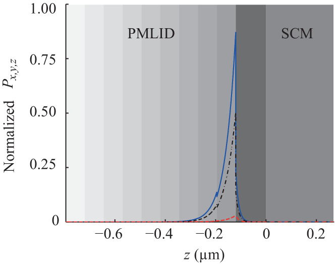
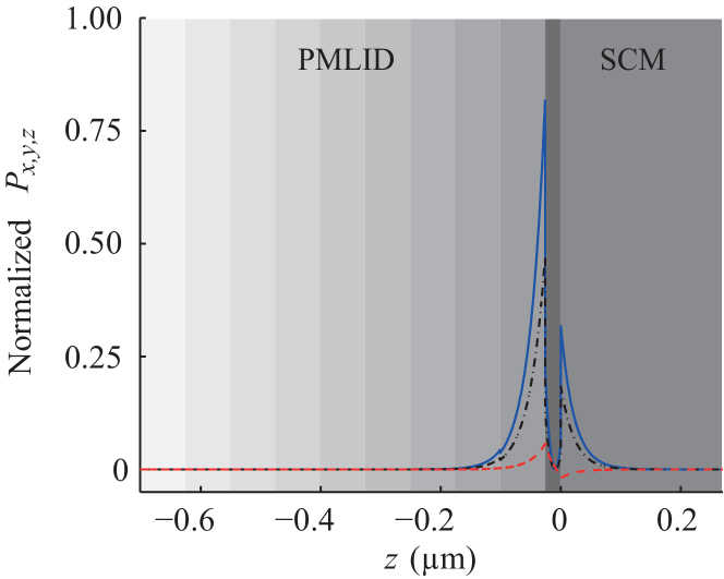
Only one ESW was found to be guided by the SCM/PMLID interface when deg. Classified as a Dyakonov–Tamm wave, its normalized wavenumber and its phase speed . Spatial variations of the Cartesian components of its time-averaged Poynting vector are presented in Figure 2.
4 CGWs guided by A/B/C structure
Now let us turn to the problem schematically illustrated in Figure 1, with materials A and C being the chosen PMLID material and SCM, respectively, while material B is isotropic and homogeneous. The thickness of the sandwiched layer was varied from to nm. With some degree of approximation, this problem can be practically implemented with the A/B/C structure of sufficiently large thickness and finite width interposed between two waveguide sections.
4.1 Planar PMLID/metal/SCM structure
Let us begin by choosing material to be silver (i.e., ). Since materials and are dielectric, the CGWs guided by this structure must be classified as compounded from SPP waves for . However, this compounding is more complicated than in two predecessor papers wherein either [34] or [33] was isotropic and homogeneous. The number of CGWs and their wavenumbers depend on due to the anisotropy of the SCM. Except in special cases, no polarization state can be assigned to any of the CGWs.
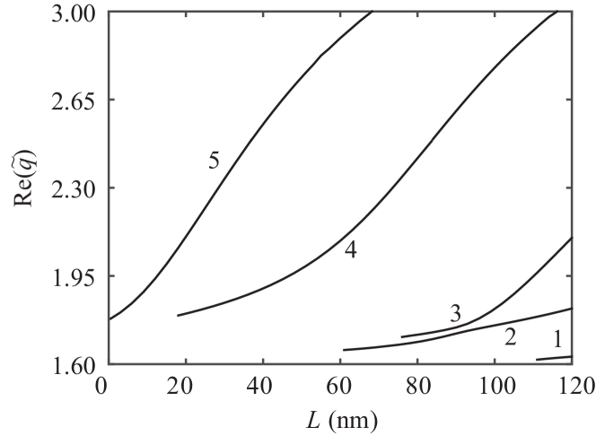
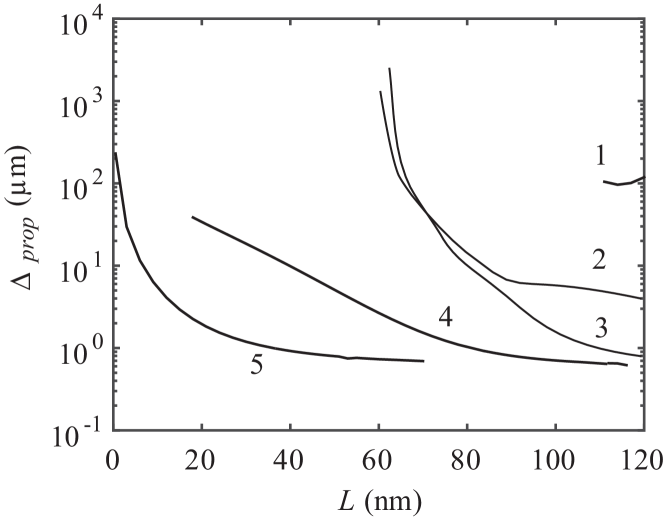
Depending on the value of nm, as many as nine different CGWs can be guided by the structure. Figures 3 and 4, respectively, show and as functions of , the wavenumbers being organized into nine different branches. Solutions on branches numbered and in the figures have phase speeds exceeding , whereas the other seven branches have solutions with phase speeds below .

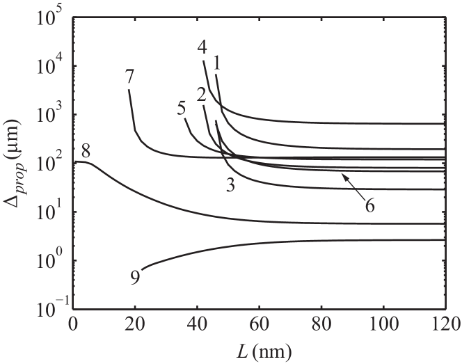
For metal thickness significantly greater than the skin depth nm of silver, and assume steady values. Their values for the thickest metal layer considered ( nm) are reported in Table 8. In that table, solutions 1, 4, 6, and 9 are practically the same as for the -polarized SPP waves guided by the PMLID/metal interface alone (see Table 5); solutions 2, 5, and 7 are almost the same as for the -polarized SPP waves guided by the PMLID/metal interface alone (see Table 5); and solutions 3 and 8 are almost the same as for the SPP waves guided by planar metal/SCM interface alone (see Table 3). In other words, the PMLID/metal and metal/SCM interfaces in the PMLID/metal/SCM structure are virtually decoupled from each other for .
This decoupling is evident in the spatial distributions of plotted in Figs. 5, and 6 for solutions 8, and 9 for nm and deg. The CGWs are bound to either the PMLID/metal interface or the metal/SCM interface, but not to both.
| Soln. | Re | Im | (m) | (nm) | |
|---|---|---|---|---|---|
| 1 | |||||
| 2 | |||||
| 3 | |||||
| 4 | |||||
| 5 | |||||
| 6 | |||||
| 7 | |||||
| 8 | |||||
| 9 |
Coupling of the PMLID/metal and metal/SCM interfaces enhances as is diminished. Each solution branch in Figs. 3 and 4 exists only for , the threshold value for each branch (except branch 9) being reported in the last column of Table 8. We were unable to determine for solution branch 9, because exceeded as decreased below nm and thus fell out of the range .
Solution branches 1 to 6 have nm, implying relatively weak coupling between the PMLID/metal and metal/SCM interfaces for . Still, Figs. 3 and 4 indicate that is substantially impacted by the coupling for .
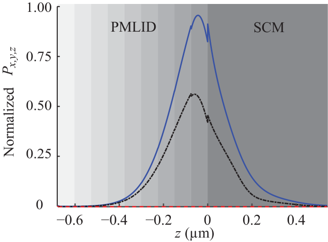
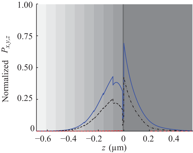
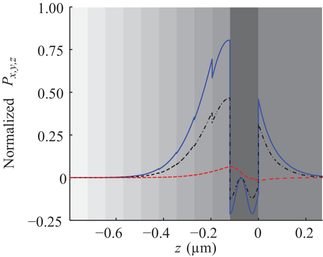
Solution branch 9 exists for , indicating stronger coupling between the two interfaces. This is confirmed by the plots of versus for nm in Fig. 7. Clearly, both the PMLID material and the SCM carry the energy of the CGW, the former more than the latter. Thus, the characteristics of SPP waves of two different types have been mixed in the CGW. SPP waves of one type are guided by the PMLID/metal interface and have specific polarization states, whereas no polarization state can be assigned for SPP waves of the other type as they are guided by the metal/SCM interface [16, 44]. Similar conclusions can be drawn for solution branch 7 as well, for which .
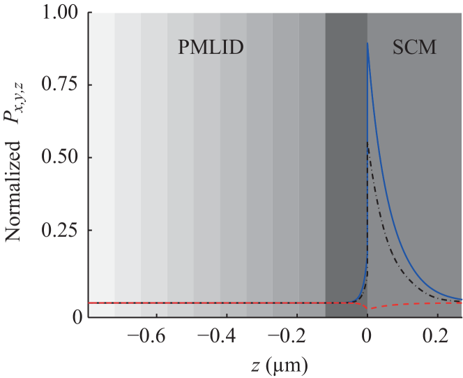
Finally, solution branch 8 has . Hence, solutions must exist even if , which is indicative of very strong coupling between the PMLID/metal and metal/SCM interfaces. The strong coupling is very clear in the spatial profile of presented in Fig. 8 for nm, with the energy of the CGW carried almost equally by the PMLID material and the SCM.
Furthermore, when , the PMLID/metal/SCM structure collapses into the PMLID/SCM structure, on the solution branch 8 in Figs. 3 and 4 acquires the purely real value , the spatial variations of the Cartesian components of the time-averaged Poynting vector of the CGW are the same as presented in Figure 2. and the CGW converts into the Dyakonov–Tamm wave discussed in Sec. 3.7.
4.2 Planar PMLID/dissipative-HID/SCM structure
When material B is the nonplasmonic analog of silver (i.e., ), as many as five different CGWs can be guided by the PMLID/dissipative-HID/SCM structure for nm and deg. These CGWs for are compounded from Uller–Zenneck waves of Secs. 3.3 and 3.6; alternatively, they are compounded from the Dyakonov–Tamm waves of Sec. 3.3.3 and the Tamm waves of Sec. 3.6.
Figures 9 and 10 show Re and as functions of nm, respectively. The solutions are organized into five different branches. On every branch, both and decrease as increases. No solutions with phase speed exceeding were found, most likely because (i) although the PMLID/dissipative-HID interface alone does support high-phase-speed Uller–Zenneck (or Tamm) waves (see Table 6), the SCM/dissipative-HID interface alone does not support high-phase-speed Uller–Zenneck (or Dyakonov–Tamm) waves (see Table 4, and (ii) is much smaller than the skin depth nm in .
Values of and when nm are reported in Table 9. In this table, solutions and have values very close to those for two -polarized Uller–Zenneck waves guided by the PMLID/dissipative-HID interface alone (see Table 6); solutions , , and have values very close to those for the –polarized Uller–Zenneck waves guided by the PMLID/dissipative-HID interface alone (see Table 6); and solution has a value very close to that for an Uller–Zenneck wave guided by planar SCM/dissipative-HID interface alone (see Table 4). Solutions and in Table 9 are somewhat, but not very, close to a solution in Table 4 and a solution in Table 6, indicating that the two interfaces are coupled even for . Their decoupling would require even larger values of the ratio .
| Soln. | Re | Im | (m) | |
|---|---|---|---|---|
Whereas the number of solution branches is five in Figs. 9 and 10 for nm, the number of solutions is eight in Table 9 for nm. Eight must be the largest number of solutions possible, based on the data in Tables 4 and 6. Since each solution branch will exist only for , three solution branches must have nm.
Figure 11 present the spatial profiles of for solution 2 in Figure 9 when nm. A fraction of the energy of the CGW resides in both the PMLID material and the SCM, with the former carrying more energy than the latter. Clearly then, the characteristics of Uller–Zenneck waves of two different types have been mixed in the CGW. Uller–Zenneck waves of one type (alternatively, Tamm waves) are guided by the PMLID/dissipative-HID interface and have specific polarization states, whereas no polarization state can be assigned for Uller–Zenneck waves of the other type (alternatively, Dyakonov–Tamm waves) as they are guided by the dissipative-HID/SCM interface [28, 16]. Similar conclusions hold for the other four solution branches in Figure 9.
4.3 Planar PMLID/nondissipative-HID/SCM structure
When material B is nondissipative (i.e., ), only one solution was found in the range nm. Figure 12 depicts as a function of . Since all the materials involved are nondissipative is obviously real-valued so that, theoretically, and the CGW wave can propagate indefinitely. As discussed in Sec. 3.6, there will always be some dissipation so that can be large but not infinite.
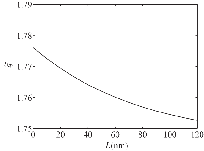
For a glass layer much thicker than nm (i.e., nm), two solutions were found. Their values, reported in Table 10, are the same as for the Tamm waves guided by the PMLID/glass interface alone (Table 7) in Sec. 3.6. Solution 2 in Table 10 is the asymptotic value of the curve in Figure 12 as the thickness of the glass layer increases, whereas solution 1 has obviously a threshold value nm.
| Solution | ||
|---|---|---|
| 1 | ||
| 2 |
It is worth pointing out that the solutions found for the PMLID/nondissipative-HID/SCM structure for large are the same as for the PMLID/nondissipative-HID interface alone. Because the HID is nondissipative (i.e., the skin depth is infinite), this observation means that the coupling between the two interfaces of the sandwiched layer is not only affected by the ratio but also by the rates at which the fields of the ESWs guided individually by the two interfaces decay away from the respective guiding interfaces.
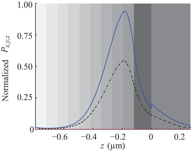
Even when the skin depth is infinite, a strong coupling between the PMLID/nondissipative-HID and the nondissipative-HID/SCM interfaces is expected for nm. This is confirmed by the plot of vs. for nm in Figure 13. Clearly, both the PMLID and the SCM carry the energy of the CGW, the former more than the latter, and the characteristics of Tamm and Dyakonov–Tamm waves have been mixed in the CGW [16, 28, 19].
5 Concluding remarks
We solved the boundary-value problem for electromagnetic waves guided by a layer of a homogeneous and isotropic (metal or dielectric) material sandwiched between a structurally chiral material and a periodically multi-layered isotropic dielectric material. Though this problem is practically unimplementable sensu strictissimo because it involves two half spaces, it provides information on the propagation distance, otherwise unachievable. But it can be implemented in an approximate sense, with a PMLID/sandwiched-material/SCM structure of sufficiently large thickness and finite width interposed between two waveguide sections.
We found that compound guided waves can propagate bound to both interfaces of the sandwiched material with energy distributed in both the SCM and the PMLID materials, if the sandwiched layer is sufficiently thin. Hence, CGWs that mix together the characteristics of SPP waves, Tamm waves, Dyakonov–Tamm waves, and Uller–Zenneck waves are theoretically possible, exemplifying the inherent commonality between these electromagnetic surface waves. A multiplicity of CGWs can exist, depending on the thickness of the sandwiched layer. All of them differ in phase speed, attenuation rate, and field profile, even though all are excitable at the same frequency. For any thickness of the sandwiched layer, at least one CGW exists.
The coupling between the two faces of the sandwiched layer, giving rise to CGWs, is affected by two distinct mechanisms: (i) the ratio of the thickness of the sandwiched layer to the skin depth in that material and (ii) the rates at which the fields of the ESWs guided individually by the two interfaces decay away from their respective guiding interfaces.
Finally, CGWs have been found for an all-dielectric-configuration where the materials used can even be extremely weakly dissipative. Such a configuration could be very useful for sensing applications in special cases where the presence of a metal is unwanted, e.g. in an electrically hazardous environment.
References
- [1] K. Uller, Beiträge zur Theorie der Elektromagnetischen Strahlung, Ph.D. thesis (Universität Rostock, 1903), Chap. XIV.
- [2] J. R. Wait, “The ancient and modern history of EM ground-wave propagation,” IEEE Antennas Propagat. Mag. 40(5), 7–24 (1998).
- [3] N. Tesla, ”Art of transmitting electrical energy through natural mediums,” US Patent 787412 (filed on May 16, 1900; published on April 18, 1905).
- [4] J. Zenneck, “Über die Fortpflanzung ebener elektromagnetischer Wellen längs einer ebenen Lieterfläche und ihre Beziehung zur drahtlosen Telegraphie,” Ann. Phys. Lpz. 23, 846–866 (1907).
- [5] A. Sommerfeld, “Über die Ausbreitung der Wellen in der drahtlosen Telegraphie,” Ann. Phys. Lpz. 28, 665–736 (1909).
- [6] A. Sommerfeld, “Über die Ausbreitung der Wellen in der drahtlosen Telegraphie,” Ann. Phys. Lpz. 62, 95–96 (1920).
- [7] A. Sommerfeld, “Über die Ausbreitung der Wellen in der drahtlosen Telegraphie,” Ann. Phys. Lpz. 81, 1135–1153 (1926).
- [8] M. Faryad and A. Lakhtakia, “Observation of the Uller–Zenneck wave”, Opt. Lett. 39, 5204–5207 (2014).
- [9] R. H. Ritchie, “Plasma losses by fast electrons in thin films,” Phys. Rev. 106, 874–881 (1957).
- [10] T. Turbadar, “Complete absorption of light by thin metal films,” Proc. Phys. Soc. Lond. 73, 40–44 (1959).
- [11] A. Otto, “Excitation of nonradiative surface plasma waves in silver by the method of frustrated total reflection,” Z. Phys. 216, 398–410 (1968).
- [12] E. Kretschmann and H. Raether, “Radiative decay of nonradiative surface plasmons excited by light,” Z. Naturforsch. A 23, 2135–2136 (1968).
- [13] J. M. Pitarke, V. M. Silkin, E. V. Chulkov, and P. M. Echenique, “Theory of surface plasmon and surface-plasmon polaritons,” Rep. Prog. Phys. 70, 1–87 (2007).
- [14] I. Abdulhalim, M. Zourob, and A. Lakhtakia, “Surface plasmon resonance for biosensing: A mini-review,” Electromagnetics 28, 214–242 (2008).
- [15] J. Zhang, L. Zhang, and W. Xu, “Surface plasmon polaritons: Physics and applications,” J. Phys. D: Appl. Phys. 45, 113001 (2012).
- [16] J. A. Polo Jr., T. G. Mackay, and A. Lakhtakia, Electromagnetic Surface Waves: A Modern Perspective, (Elsevier, Waltham, MA, USA, 2013).
- [17] L. Liu, M. Faryad, A. S. Hall, G. D. Barber, S. Erten, T. E. Mallouk, A. Lakhtakia, and T. S. Mayer, “Experimental excitation of multiple surface-plasmon-polariton waves and waveguide modes in a one-dimensional photonic crystal atop a two-dimensional metal grating,” J. Nanophoton. 9, 093593 (2015).
- [18] G. J. Sprokel, “The reflectivity of a liquid crystal cell in a surface plasmon experiment,” Mol. Cryst. Liq. Cryst. 68, 39–45 (1981).
- [19] P. Yeh, A. Yariv, and C.-S. Hong, “Electromagnetic propagation in periodic stratified media. I. General theory,” J. Opt. Soc. Am. 67, 423–438 (1977).
- [20] P. Yeh, A. Yariv, and A. Y. Cho, “Optical surface waves in periodic layered media,” Appl. Phys. Lett. 32, 104–105 (1978).
- [21] M. Shinn and W. M. Robertson, “Surface plasmon-like sensor based on surface electromagnetic waves in a photonic band-gap material,” Sens. Actuat. B: Chem. 105, 360–364 (2005).
- [22] V. N. Konopsky and E. V. Alieva, “Photonic crystal surface waves for optical biosensors,” Anal. Chem. 79, 4729–4735 (2007).
- [23] F. N. Marchevskiĭ, V. L. Strizhevskiĭ, and S. V. Strizhevskiĭ, “Singular electromagnetic waves in bounded anisotropic media,” Sov. Phys. Solid State 26, 911–912 (1984).
- [24] M. I. D’yakonov, “New type of electromagnetic wave propagating at an interface,” Sov. Phys. JETP 67, 714–716 (1988).
- [25] O. Takayama, L. Crasovan, D. Artigas, and L. Torner, “Observation of Dyakonov surface waves,” Phys. Rev. Lett. 102, 043903 (2009).
- [26] O. Takayama, L.-C. Crasovan, S. K. Johansen, D. Mihalache, D. Artigas, and L. Torner, “Dyakonov surface waves: A review,” Electromagnetics 28, 126–145 (2008).
- [27] O. Takayama, D. Artigas, and L. Torner, “Lossless directional guiding of light in dielectric nanosheets using Dyakonov surface waves,” Nature Nanotechnol. 9, 419–424 (2014).
- [28] A. Lakhtakia and J. A. Polo Jr., “Dyakonov–Tamm wave at the planar interface of a chiral sculptured thin film and an isotropic dielectric material,” J. Eur. Opt. Soc. Rapid Publ. 2, 07021 (2007).
- [29] A. Lakhtakia and M. Faryad, “Theory of optical sensing with Dyakonov–Tamm waves,” J. Nanophoton. 8, 083072 (2014).
- [30] E. N. Economou, “Surface plasmons in thin films,” Phys. Rev. 182, 539–554 (1969).
- [31] L. Wendler and R. Haupt, “An improved virtual mode theory of ATR experiments on surface polaritons: Application to long-range surface plasmon-polaritons in asymmetric layer structures,” phys. stat. sol. (b) 143, 131–148 (1987).
- [32] F. Yang, J. R. Sambles, and G. W. Bradberry, “Long-range surface modes supported by thin films,” Phys. Rev. B 44, 5855–5872 (1991).
- [33] F. Chiadini, V. Fiumara, A. Scaglione, and A. Lakhtakia, “Composite surface-plasmon-polariton waves guided by a thin metal layer sandwiched between a homogeneous isotropic dielectric material and a periodically multilayered isotropic dielectric material,” J. Nanophoton. 9, 093060 (2015).
- [34] F. Chiadini, V. Fiumara, A. Scaglione, and A. Lakhtakia, “Compound surface-plasmon-polariton waves guided by a thin metal layer sandwiched between a homogeneous isotropic dielectric material and a structurally chiral material,” Opt. Commun. 363, 201–206 (2016).
- [35] M. Faryad and A. Lakhtakia, “Multiple surface-plasmon-polariton waves localized to a metallic defect layer in a sculptured nematic thin film,” Phys. Status Sol. RRL 4, 265–267 (2010).
- [36] M. Faryad and A. Lakhtakia, “Propagation of surface waves and waveguide modes guided by a dielectric slab inserted in a sculptured nematic thin film,” Phys. Rev. A 83, 013814 (2011).
- [37] O. Takayama, D. Artigas, and L. Torner, “Coupling plasmons and dyakonons,” Opt. Lett. 37, 1983–1985 (2012).
- [38] P. W. Baumeister, Optical Coating Technology (SPIE Press, Bellingham, WA, USA, 2004).
- [39] I. J. Hodgkinson and Q. h. Wu, Birefringent Thin Films and Polarizing Elements (World Scientific, Singapore, 1997).
- [40] A. Lakhtakia and R. Messier, Sculptured Thin Films: Nanoengineered Morphology and Optics (SPIE, Bellingham, WA, USA , 2005).
- [41] P. G. de Gennes and J. A. Prost, The Physics of Liquid Crystals, 2nd ed. (Clarendon Press, Oxford, United Kingdom, 1993).
- [42] M. Faryad, A. S. Hall, G. D. Barber, T. E. Mallouk, and A. Lakhtakia, “Excitation of multiple surface-plasmon-polariton waves guided by the periodically corrugated interface of a metal and a periodic multilayered isotropic dielectric material,” J. Opt. Soc. Am. B 29, 704–713 (2012).
- [43] I. Hodgkinson, Q. h. Wu, and J. Hazel, “Empirical equations for the principal refractive indices and column angle of obliquely deposited films of tantalum oxide, titanium oxide, and zirconium oxide,” Appl. Opt. 37, 2653–2659 (1998).
- [44] J. A. Polo Jr., T. G. Mackay, and A. Lakhtakia, “Mapping multiple surface-plasmon-polariton-wave modes at the interface of a metal and a chiral sculptured thin film,” J. Opt. Soc. Am. B 28, 2656–2666 (2011).
- [45] M. R. M. Atalla, M. Faryad, and A. Lakhtakia, “On surface-plasmon-polariton waves guided by the interface of a metal and a rugate filter with a sinusoidal refractive-index profile. Part II: High-phase-speed solutions,” J. Opt. Soc. Am. B 29, 3078–3086 (2012).