Molybdenum Disulphide Nanoflakes Grown by Chemical Vapour Deposition on Graphite: Nucleation, Orientation, and Charge Transfer
Abstract
Two-dimensional molybdenum disulphide on graphene grown by chemical vapour deposition is a promising van der Waals system for applications in optoelectronics and catalysis. To extend the fundamental understanding of growth and intrinsic properties of molybdenum disulphide on graphene, molybdenum disulphide on highly oriented pyrolytic graphite is a suitable model system. Here we show, experimentally and by density-functional-theory calculations, that molybdenum disulphide flakes grow in two orientations. One of the orientations is energetically preferred, the other one is rotated by 30 degree. Because of a high energy barrier confirmed by our calculations both orientations are stable at room temperature and their switching can only be forced by external stimuli, i.e. by a scanning tunneling microscope tip. Combined Kelvin probe microscopy and Raman spectroscopy measurements show that the flakes with a typical size of a few hundred nanometers are less doped than the often studied exfoliated molybdenum disulphide single layer.
1 Introduction
Two-dimensional (2D) materials have become tremendously attractive research topics due to their extraordinary properties. Above all, graphene with its extraordinary thermal [1, 2], electrical [3] and mechanical [4] properties promises to revolutionize many applications. On the other hand, one of the biggest disadvantages for (opto)electronics is the zero band gap of graphene [5]. Other 2D materials such as molybdenum disulphide (MoS2) have a band gap in the visible range [6, 7], but also a much lower conductivity [8].
A combination of both materials, a so-called van der Waals heterostructure, can overcome their respective disadvantages by combining the advantages of both materials. The high conductivity of graphene together with the band gap of MoS2 enables effective photoelectric devices [9, 10, 11]. Graphene and MoS2 based heterostructures are also potentially used in sensing [12, 13], spintronics [14], or as memory devices [15]. Such feasibility studies are performed with exfoliated 2D materials and recently also with 2D materials from chemical vapour deposition (CVD), which allows upscaling to large scale and flexible devices [16, 17]. To fabricate such heterostructure devices often stacking [18, 19] and transfer techniques [20, 21] are used. In contrast, direct growth of heterostructures provides a clean interface, but will at the same time have an effect on the physical properties.
In order to acquire a fundamental understanding of the growth and the intrinsic properties of MoS2 on graphene, highly oriented pyrolytic graphite (HOPG) can be used as a model substrate. The HOPG surface has the same atomic surface structure as graphene and can be prepared much cleaner and with a lower defect density than the surface of CVD graphene, making HOPG ideal for studying the growth and the physical properties of MoS2 on a sp2 hybridized carbon surface.
When MoS2 is grown by CVD, triangular islands – which are called (nano)flakes in the following – are typically formed. This particular shape is helpful in determining crystal orientations. Indeed, on graphite and on graphene preferred orientations of the MoS2 flakes were found [22, 23, 24, 25]. It is typically observed that MoS2 flakes are rotated to each other by a multiple of 60 degrees, but in a few publications a rare orientation right inbetween has been reported. This has been experimentally shown by Liu et al. in the most comprehensive study [22]: Grazing-incidence wide-angle X-ray scattering proves that two orientations indeed occur for MoS2 on epitaxial graphene (on silicon carbide) in different frequencies. The dominant orientation could be assigned to the case where the armchair direction of the MoS2 flakes is aligned to the armchair direction of the underlying graphene layer. In the less frequent orientation, the zigzag direction of one lattice and the armchair direction of the other lattice correlate. On HOPG these orientation study have been done by comparing neighboring flakes in scanning probe microscope (SPM) images. Thereby it was found that MoS2 grows mainly at the HOPG step edges [23, 24, 25]. While experimental data on structure and growth is thus available, theoretical calculations elucidating the driving force behind the orientation behaviour are missing. Furthermore, studies regarding the charge transfer in MoS2-based heterostructures are still rare. This is surprising as for many of the proposed electrical devices based on MoS2-graphene heterostructures the electronic properties, such as carrier concentration (correlated with the Fermi level or doping), are a key factor.
In this paper, we address these issues and study ultrathin MoS2 on HOPG in order quantify the carrier concentration in MoS2. The paper is organized as follows: We first present structural data from our system and discuss an unexpected correlation between MoS2 growth and the HOPG step height which we found by evaluating atomic force microscope (AFM) images. We then present an explanation for the experimentally observed MoS2 flake orientation based on results from DFT calculations. Finally, we discuss the charge carrier concentration in MoS2 which we derive by combining Raman and KPFM measurements.
2 Methods
2.1 Growth Process
The samples were produced in a custom made process system for CVD of MoS2 based on the system reported by Lee et al. [26] and described in detail in our previous work [27]. Our process system consists of a quartz tube with two heating zones provided by a heating belt and a tube furnace (ThermConcept ROS 38/250/12). With this setup the two heating zones can be used with different temperatures to evaporate the molybendum source (MoO3 powder, Alfa Aesar, 99.95%) and the sulphur source (S powder, Sigma Aldrich, 99.98%) separately. During the process inert Ar gas flows through the tube. Within the upstream heating zone of the heating belt a crucible containing sulphur powder is placed. In the second heating zone provided by the tube furnace a crucible with MoO3 powder (upstream) and an HOPG crystal (downstream) is placed.
The recipe is as follows: 200 mg sulphur powder and 20 mg MoO3 powder are used. A freshly cleaved HOPG crystal is placed 3 cm downstream from the molybdenum source. The heating rate of the tube furnace is 480 °C/min to reach the maximum temperature of 650 °C. When the furnace is started, the heating belt is activated with a temperature of about 70 °C to pre-anneal the sulphur powder and the Ar flow is set to 25 Ncm3/min. Fifteen minutes before the furnace reaches the maximum temperature the belt is set to 150 °C and the Ar flow to 200 Ncm3/min. While the heating zones stay at the maximum temperature a pressure of 6 mbar is measured in the quartz tube. Five minutes after the furnace has reached the maximum temperature the furnace and the belt are switched off to cool the system down. In this procedure MoS2 single layers grow on the face-down side in the microcavity between HOPG crystal and crucible.
2.2 Characterization
The samples are characterized with a SPM operating in a RHK UHV 7500 system with a base pressure of about 4 * 10-10 mbar. This ensures that the influence of contaminations during measurements is mimimized. The SPM is controlled by the fully integrated system for digital signal processing RHK R9. The system is used to perform non-contact atomic force microscopy (NC-AFM) and Kelvin probe force microscopy (KPFM) simultaneously, and scanning tunneling microscopy (STM). For NC-AFM and KPFM commercial tips are used (Nanoworld NCH). The tips for performing STM are etched with the lamella method, for which a tungsten wire and a 5 molar NaOH solution are used. The Raman spectra are recorded using a Renishaw InVia Raman microscope at the Interdisciplinary Center for Analytics on the Nanoscale (ICAN, core facility funded by the German Research Foundation, DFG). The laser wavelength is 532 nm and the spot diameter is 1 µm. The laser power was kept at 200 µW to avoid damage. The Raman microscope was calibrated on a silicon sample with a Si Raman mode at 520.78 cm-1.
3 Results and Discussion
3.1 Growth morphology and nucleation
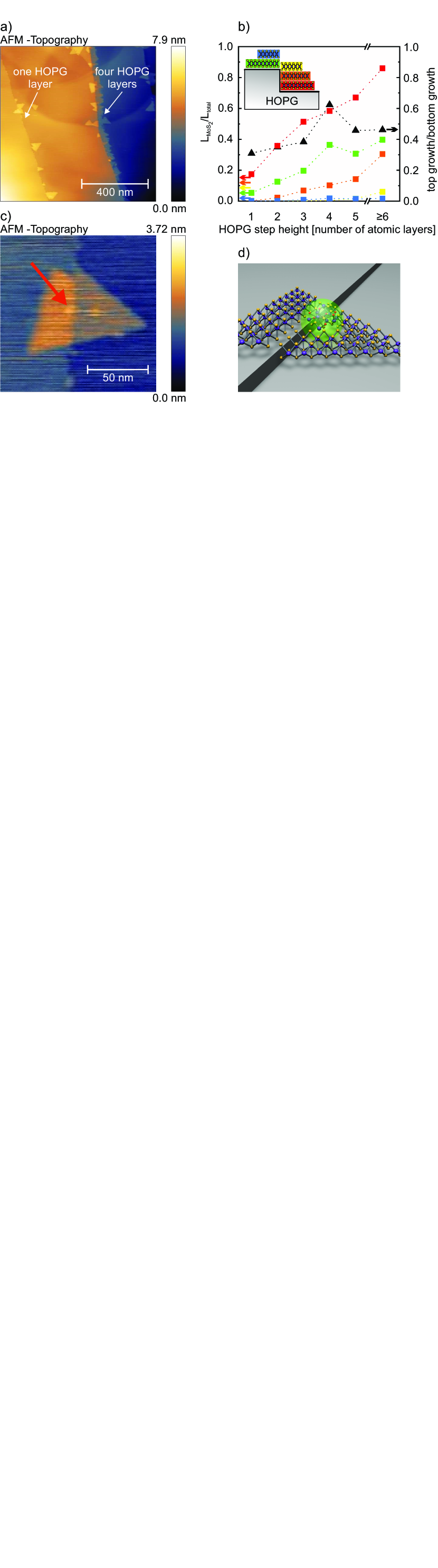
Our investigations have shown that MoS2 does not grow as a continuous film on graphene, but rather in the form of islands. We start our study by discussing this peculiar growth morphology. In Fig. 1 (a) and Fig. 2 (a) AFM images of a sample after the growth procedure are shown. The HOPG surface with its typical edges of one to several atomic sp2 hybridized carbon layers is still intact. Furthermore, triangular shaped MoS2 nanoflakes with edge lengths of up to 100 nm can be observed. With the growth conditions discussed above we make two observations: (i) most of the MoS2 nanoflakes are located at the HOPG edges and (ii) are found in two orientations.
At first we discuss the preferred occurrence of the MoS2 flakes at HOPG edges, which has not been previously analysed any further to the best of our knowledge, although it is obviously crucial for growth. The AFM image in Fig. 1 (a) already gives first evidence for a correlation between the step height and the MoS2 flake height. The HOPG step edge with a height corresponding to four layers in the right half of the image is decorated by a continuous sequence of multilayer MoS2 islands, while only a few monolayer MoS2 triangles are located at the mono-atomic HOPG step edge in the left half of the image. Moreover, we observe island growth both at the upper and the lower step edge, but with more material accumulated at the lower step edge. In order to quantify this observation we analysed different areas on our sample by correlating (i) the HOPG step edge height with the MoS2 flake height and (ii) the ratio between the HOPG step length decorated with MoS2 and the total measured edge length . In total, step edges of more than 300 µm in length were evaluated. The result is shown in Fig. 1 (b), where is plotted versus the HOPG step height in atomic layer numbers. Different colours indicate whether the MoS2 flakes had grown on the lower (red, orange, yellow) or on the upper terrace (green, blue) of the HOPG step edge (see illustration in the inset of Fig. 1 (b)). The dashed lines are included to guide the eye. The results show a clear correlation between the HOPG step edge height and the MoS2 flake height, and the ratio , respectively, and thus the total amount of grown MoS2.
The observation that the MoS2 flake height differs on the upper and the lower side of the HOPG step edge indicates that the step edges constitute barriers for materials transport, a phenomenon known as the Ehrlich-Schwöbel effect [28, 29, 30]. It remains to be discussed to what extent the results for the ratio could be affected by overgrowth, i.e., an MoS2 island could nucleate on the upper terrace and then extend to grow on top of a multilayer island of the lower terrace. Let us look at the ratio between layers grown on upper and lower terraces (black data points in Fig. 1 (b) ). This ratio is almost independent of the HOPG step height (discarding the peak at four-layers HOPG steps, see Supp. Mat. for justification). If overgrowth of islands nucleated on the upper terrace was to play a major role, one would expect a clear variation, since it would become more and more difficult to overgrow the HOPG step with increasing step height. Thus, at least for HOPG steps higher than one layer, we believe that island growth at the upper and lower ledges follows separate nucleation events.
In order to understand the observed peculiarities, we look at the possible nucleation mechanisms next. For the present case, homogeneous nucleation by random accumulations of material [31], or heterogeneous nucleation by nanoparticles (NP) [32, 31] need to be taken into consideration. It is safe to assume that these mechanism could exist simultaneously, but that their respective contribution may differ under different conditions. Other suggested mechanisms, such as so-called seeding promoters (aromatic molecules acting as artificial nucleation centers) [26, 33], or artificially induced defects by ion irradiation [34] are not applicable to our present study.
In fact, several pieces of evidence point to the role of nanoparticles as nucleation centers. For instance, Cain et al. reported MoO3-xSy nanoparticles present during the early stages of MoS2 growth, when the sulphur concentration is not high enough [32]. These nanoparticles diffuse on the surface and it is plausible that they get trapped at the HOPG step edges. Larger nanoparticles will more likely be trapped at higher step edges leading to a higher concentration there. As the layer growth starts, MoS2 flakes would preferentially grow at these nanoparticles. Since a nanoparticle may well be higher than the edge itself (see illustration in Fig. 1 (d)), it is able to promote growth of MoS2 flakes on the lower as well as on the upper terrace, in agreement with our data (see Fig. 1 (b)). This hypothesis agrees also very well with our observation that there is never growth on an upper terrace without growth on the adjoining lower terrace. In addition, the nanoparticle hypothesis is backed by our experimental observations: Figure 1 (c) shows a zoomed AFM image of a non-perfect triangular MoS2 flake. It consist of a trapezoidal part at the upper terrace and a triangular part at the lower terrace separated by the step edge. Where both flakes are touching at the position of the edge, a bright spot is seen (red arrow). A few other similar spots could be seen at the surface, but most of them are located at HOPG edges. We propose that these bright spots correspond to the nanoparticles acting as nucleation centers. During later stages of the growth, the nanoparticles could be consumed by the growth of MoS2 [31]. This explains our finding that some flakes do not have any bright spots in their centers, like the ones seen in Fig. 1 (b).
3.2 Orientation
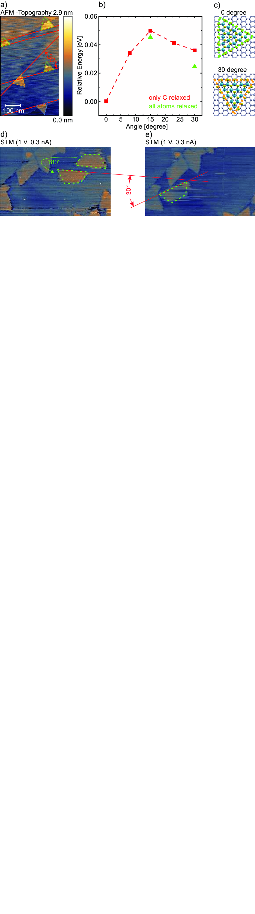
Next, we turn to the later stages of growth and look at fully developed MoS2 flakes. During growth, an epitaxial relationship concerning the orientation of the flakes is built up. To analyse this orientation, we focus on large MoS2 flakes located on HOPG terraces or single-layer steps. As marked in Fig. 2 (a) most of the MoS2 flakes are pointing in the same direction (green triangles). A significant fraction is however rotated with respect to this main orientation by either 30 degrees (orange) or 60 degrees (blue). It is noteworthy that under similar conditions MoS2 grows on (amorphous) SiO2 with edge length of several microns and without any preferential orientations [27]. Obviously, it is the crystallinity of the HOPG substrate which gives rise to the preferred orientations of the MoS2 flakes. Because of the rotational symmetry of the hexagonal graphite lattice, the orientation of the green and blue triangles corresponds to equivalent crystallographic directions. By comparing the edges of neighbouring flakes, it can be determined that the two orientations have different frequencies of occurrence (see Supp. Mat. for more AFM images). Accordingly, in Fig. 2 (a) the green/blue orientation is the preferred one and the orange the less preferred one.
It is instructive to compare our findings to observations in other van-der-Waals-bonded systems. For graphene flakes on a graphene surface, which exhibits the same sp2 hybridized carbon surface as the HOPG surface used here, it has been also experimentally shown that the flakes have a preferred orientation [35]. However, these flakes were found only in orientations of multiples of 60 degree, because minima occur in the potential landscape at these orientations [36].
To explore the potential energy surface for the MoS2-HOPG system, DFT calculations were performed (for details see Supp. Mat). To make the computations feasible, a rather small flake size (15 Mo + 50 S atoms, 1 nm edge length) has been used, and the substrate is described by a single layer of graphene instead of HOPG. Triangular flakes with Mo-edges, terminated by 100% sulphur, were cut from a two-dimensional MoS2 layer, as these edges are known to be energetically stable for the sulphur-rich environment in STM investigations of MBE grown MoS2 [Helveg.2000, Schweiger.2002]. Several registries between the MoS2 flakes and the graphene have been used as initial geometries, and the atomic positions were optimized using the forces obtained from the DFT calculations. The geometries shown in Fig. 2 (c) are the most stable configurations found in this way. Starting from these initial configurations, the flakes are rigidly rotated, allowing for optimization of the C-atom positions for each orientation.
For symmetry reasons, rotation angles in the range of 0 to 30 degree suffice, where 0 degree corresponds to orientational alignment, i.e. the armchair direction of both lattices, but also the zigzag directions (e.g. the edges of the MoS2 flakes) coincide, whereas 30 degree corresponds to a match of armchair-zigzag between both lattices. The results are shown in Fig. 2 (b), where the energy relative to the energy for the 0 degree configuration is plotted as function of the rotation angle. The figure clearly shows that the 0 degree (armchair-armchair) orientation is the energetically most favorable configuration, but there is also a local minimum for the 30 degree (armchaior-zigzag) orientation, which agrees with the experimental data of the present study and of Liu et al. [22]. The bending of the graphene sheet and the downward movement of the C atoms beneath the MoS2 flake play a significant role for the stability of the flake in both orientations. If the C atoms were not allowed to re-adjust, the increase in energy when the flake rotates from 0 to 30 degree would be considerably larger than for relaxed C atoms (cf. Supp. Mat. for more details). We learn from the calculations that the rotation goes along with an increased adsorption height of the MoS2 flake, and hence a reduced van der Waals binding energy. In large MoS2 flakes the formation of a commensurate superstructure is to be expected, as has been reported for MoSe2 on few-layer graphene [Dau.2018]. The potential energy surface has periodically repeated minima at spots where one sulphur atom sits right above a hollow site of the graphene lattice, while the neighbouring sulphur atoms are still close to neighbouring hollow sites. For the 30 degree-rotated configuration, such a favorable match is no longer possible; even in the optimized structure some fraction of the S atoms is forced to sit on top of C atoms. The steric repulsion between these atoms enforces the enhanced adsorption height in case of the rotated flake. The calculation for the condition of relaxation of all atoms (green triangle) only slightly differs from the calculation with the rigid MoS2 flake; thus the elastic response of the graphene layer to the orientation of the flake is the most crucial factor for the obtained potential landscape with local minimum at 30 degree.
The fact that the MoS2 flakes in our AFM images (Fig. 2 (a)) are also found in the less probable armchair-zigzag orientation indicates that this orientation is at least metastable at room temperature. Not even the additional force from the AFM tip is sufficient to overcome the energy barrier for a rotation of the MoS2 flakes, because a switching of flakes between two orientations has never been observed during our NC-AFM measurements. Indeed, already the very small flake modeled in Fig. 2 (c) shows a barrier at 15 degree towards rotation of 14 meV (for all atoms allowed to relax 21 meV). For realistic flakes this energy barrier will be much higher, and thus clearly exceed the thermal energy of meV at room temperature. Note that it is difficult to estimate the barrier for rotating a large flake since edge effects in the calculations for the small flakes may lead to an overestimation of the barrier when scaled to larger flakes.
Our finding that differently oriented flakes correspond to different binding energies can be further corroborated by STM measurments which can be used to force sliding and rotating MoS2 flakes across the HOPG surface (in contrast to the AFM) during imaging. To force reorientations (flips) we apply a technique reported by Feng et al., who could successfully manipulate graphene flakes on graphene by STM [35], and by Büch et al. for WS2 flakes on graphene [37]. The mechanism Feng et al. proposed for the reorientation is a vertical displacement of the flakes by the interaction with the STM tip as reported by Wong et al. [38].
Figure 2 (d) and (e) show subsequently captured STM images of our MoS2-HOPG system recorded at 1 V sample bias and 0.3 nA tunneling current of the same surface area. The flake marked in green is not fully triangular, and we can make use of its characteristic form for the following analysis. The images were recorded beginning from the upper left corner downwards and it shows that this particular flake rotates during the first image acquisition by 180 degree as depicted by the green arrow. The second image shows that the flake has rotated by a further 30 degree. In addition the flake obviously slides over the surface during the scans. As a telltale sign one can clearly see the bright stripes along the fast scan direction to the right of the marked area in Fig. 2 (e). In all cases only rotations of multiples of 30 degree were observed, which confirms our calculation of the two preferred orientations. Translations were often observed in combination with rotations. Especially flakes found in the 30 degree orientation are susceptible to translation. We observe much larger sliding distances as in the case of graphene [35], i.e. several 100 nm. That the forced flake movement and 30 degree orientation is closely interrelated confirms that the MoS2 flakes in this configuration has a binding energy to the underlying substrate which is weak enough to allow sliding of the flakes in this metastable orientation.
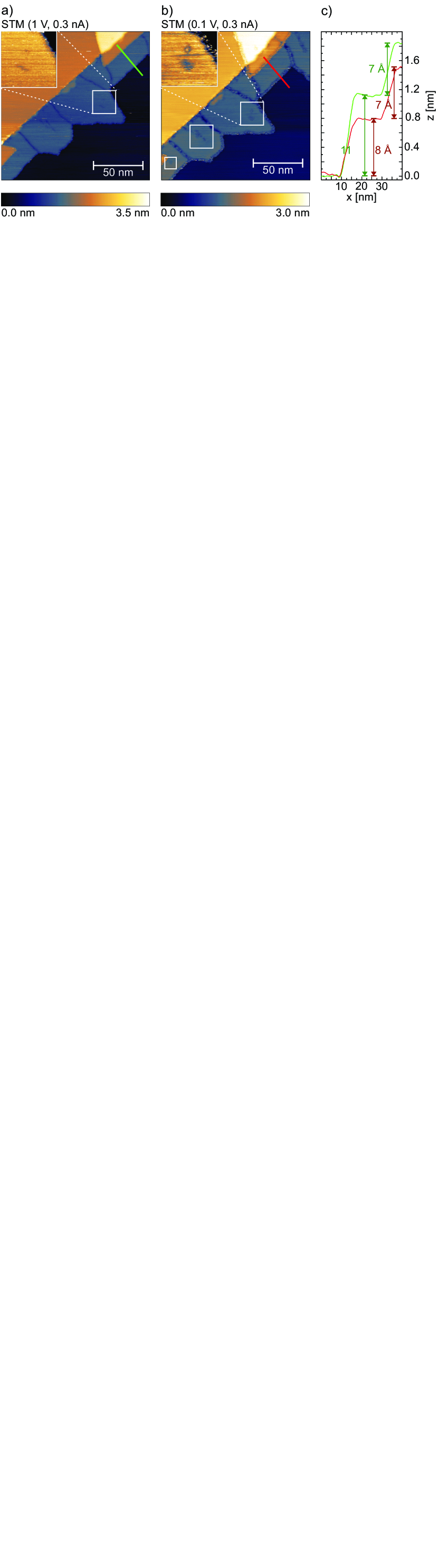
The ability of the STM tip to lift up the flake is corroborated by the fact that with STM – in contrast to NC-AFM – we frequently find single-layer MoS2 step edges which appear higher than the nominal thickness of MoS2, see Fig. 3 (a)-(c) (in addition, the different sample voltages make the STM more sensitive to either the topography Fig. 3 (a) or to the antiphase domain boundaries and defects (b), which can under certain conditions also be induced by the STM tip itself (see Supp. Mat)). This observation may be seen as an indication that the interaction of the STM tip with the MoS2 flake is comparable in strength to the interaction between MoS2 and graphite. Once the flake has been relocated by the tip into the local minimum (see Fig. 2 (c)), the global minimum can be reached at room temperature only after another tip-flake interaction to overcome the energy barrier.
3.3 Carrier concentration in MoS2
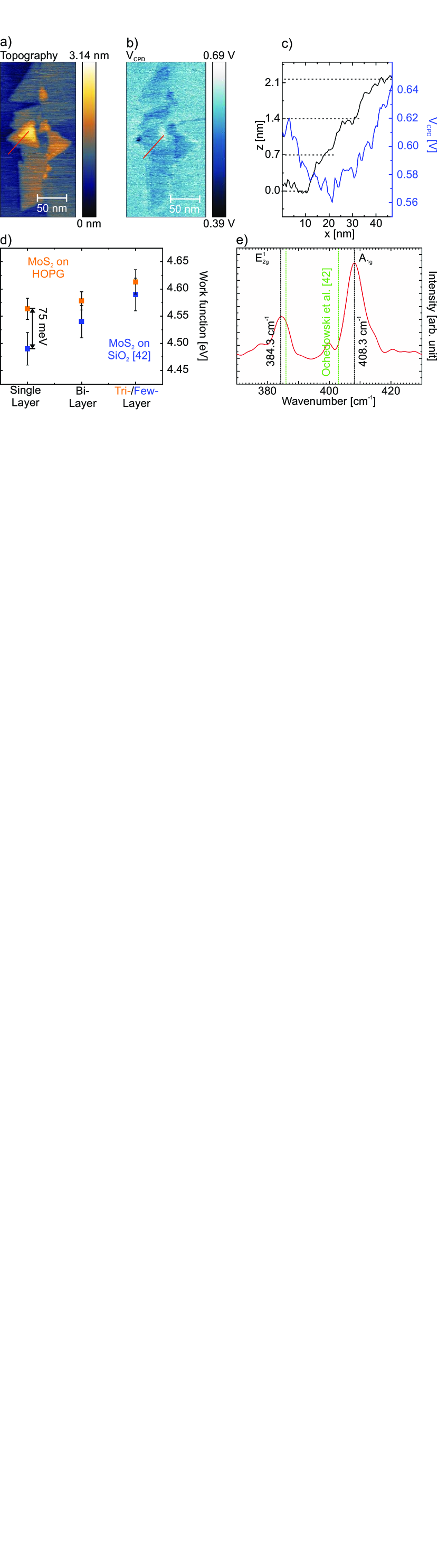
In the final section, we want to discuss the electronic properties of our samples. To this end we combined Raman spectroscopy with a laser spot size of 1 µm as an averaging technique with respect to the flake size with KPFM measurements yielding a high spatial resolution. The KPFM measurements are performed on our samples in UHV to exclude any influence of the environment [39]. Fig. 4 (b) shows the contact potential difference () image of single layer, bilayer, and trilayer MoS2 flakes, which are clearly seen in the topographic image in Fig. 4 (a). In the image a material contrast between MoS2 and HOPG is observable. The single layer and bilayer areas are almost indistinguishable, while the trilayer has an increased value with respect to the HOPG surface. The linescans in Fig. 4 (c) obtained along the red line in the topography and images show this more clearly. The dotted lines indicate the MoS2 layer height of about 0.7 nm, which confirms the number of MoS2 layers in the image.
Because the work function of HOPG is very well known and HOPG is inert, we can easily calibrate our data against this value. With = 4.6 eV [40] we obtain the following work function for single layer 4.564 0.02 eV, for bilayer 4.578 0.02 eV, and for trilayer MoS2 4.613 0.02 eV. These values are in good agreement with the study of Precner et al. on MoS2 on HOPG [41]. In order to classify the obtained values in terms of the relative charge transfer our results are compared with the work function of exfoliated MoS2 flakes on SiO2, which have been characterized under similar conditions with the same KPFM technique [39], see Fig. 4 (d). In both cases, MoS2 on HOPG and MoS2 on SiO2, the work function increases with the number of layers. However, the work function for single layer MoS2 on HOPG is shifted towards higher values by approximately 75 meV. The Fermi level and, by implication, the work function too, can be related to the electron density . Thus, we find that in the case of MoS2 on HOPG electrons are effectively depleted in the MoS2 layer in comparison to MoS2 on SiO2.
In order to quantify the KPFM data the relation for the Fermi level of a non-degenerate semiconductor to its electron density is used: , with the intrinsic Fermi level, the temperature and the Boltzmann constant. Thus, the charge carrier density can only be determined with respect to the intrinsic Fermi level and the intrinsic electron density . Although and are unknown, the ratio as the doping concentration ratio between MoS2 supported by HOPG and by SiO2 can be determined. For single layer MoS2 with a Fermi level change of 75 meV we obtain a ratio of 0.055. This means, that the electron density in MoS2 on SiO2 due to doping by charge transfer is one to two orders of magnitude higher than in MoS2 on HOPG.
Without or the relative order of magnitude of the doping of both systems can be determined, but the absolute number of the order of magnitude remains unknown. Therefore, Raman measurements are performed. The spectra shown in Fig. 4 (e) exhibit the characteristic peaks for MoS2: the E and the A1g mode are found at 384.3 cm-1 and 408.3 cm-1, respectively. Because several AFM images (e.g. Fig. 1 (a)) and also the diagram in Fig. 1 (b) show that the most part of the MoS2 film has grown as single layer, we take the average Raman signal from several such small flakes and again compare this data with data taken from larger single layer MoS2 flakes exfoliated on SiO2. There are several Raman studies on MoS2 on SiO2, including that by Lee et al. [42] and own previous studies [39, 27]. Taking into account and adjusting different offsets during calibration, the E and the A1g mode for MoS2 on SiO2 can be found in the range of 384.6 - 386.5 cm-2 and 403 - 405.4 cm-2, respectively. For quantitative analysis, the Raman data of Ochedowksi et al. are used for comparison, as this was already used as a comparative study for the KPFM data [39]. These reference peak positions at 386.1 cm-2 and 403.0 cm-2 are plotted with a green dotted line in the diagram of Fig. 4 (e). The slightly lower A1g mode in contrast to other studies may originate from pre-processing of the SiO2 substrate in this particular study. The peak difference for MoS2 on HOPG is obviously larger than for MoS2 on SiO2. A Raman peak shift of the MoS2 modes can have different origins. Apart from the number of MoS2 layers [42], e.g. strain [43, 27] and electronic doping [44] are known to affect the peak positions in different ways. The latter affects almost exclusively the A1g mode, while strain is more influential on the E mode, and the layer number affects both Raman modes. In qualitative terms, this means that MoS2 on HOPG is more stretched (or less compressed) and undergoes electron depletion with respect to MoS2 on SiO2.
The linear dependency of the Raman mode shift on both, strain and electron accumulation, experimentally and theoretically determined and reported by Rice et al. [43] and Chakraborty et al. [44], respectively, allows a rapid quantitative analysis of the data. The E mode shifts by cm-2 per % of strain and by 0.6 cm-2 per electron accumulation of cm-2, the A1g mode shifts by cm-2 per % of strain and by 4 cm-2 per electron accumulation of cm-2. Based on their data, we can estimate a relative strain of 1.3 % and the change of electron density for the MoS2-HOPG system with respect to the MoS2-SiO2 system to be /cm2. As our Raman microscope averages over several flakes within one measurement and a Raman shift could be due to contributions from few-layer MoS2, this value may not be exact but will be correct within the order of magnitude. Combined with the estimation from the KPFM data we find the doping of MoS2 on SiO2 to be on the order of 1013/cm2, while the doping of MoS2 on HOPG is on the order of 1012/cm2.
We propose that this difference is due to the following reasons: The high concentration of impurities in SiO2 and the intercalated water film, which is typical for exfoliated flakes, leads to a different charge-transfer into the MoS2 from the SiO2 than from the HOPG. In contrast, those doping mechanisms are absent on the clean HOPG surface. The MoS2 layers were grown on the HOPG substrate under such high temperatures that no water film is intercalated, therefore the layer thickness of the first MoS2 layer corresponds to the expected value of about 0.7 nm, see Fig. 4 (c). Thus, MoS2 on a quasi pristine and conductive HOPG surface is much closer to its intrinsic electronic state. Note that we do not know the intrinsic Fermi level nor the intrinsic charge carrier concentration. A much stronger hole doped MoS2 on HOPG with respect to MoS2 on SiO2 would also be in agreement with our data.
Another possible reason for the difference in the doping level is that CVD MoS2 may have a higher defect density than exfoliated MoS2. The formation of sulfur vacancies is much more likely than molybdenum vacancies in CVD and exfoliated MoS2 [45, 46, 47]. These sulfur vacancies have no influence on the doping sensitive Raman mode of single layer MoS2 [48] and as a consequence would escape our analysis here. Furthermore, various photoluminescence studies have shown that intercalated water on the SiO2 substrate has a strong electron doping influence on single layer MoS2 [49, 50, 51] rendering the different substrate and environment of the MoS2 to be the most likely reason of the different carrier concentration.
4 Summary
Van der Waals heterostructures with their peculiar interface properties offer new opportunities for novel device architectures. Their fabrication poses however still a challenge as stacking and transfer techniques come along with rather ill-defined inter- and surfaces. Direct growth of such heterostructures provides an excellent alternative in this respect but optimum growth parameters as well as properties remain to be investigated. In this work, two-dimensional MoS2 has been grown directly on HOPG by CVD and studied by complementary methods. A self-seeding nucleation process was identified to be at the origin of the growth mechanism. We found two stable flake orientations which could be assigned by our DFT results to the more frequent armchair-armchair configuration and the less frequent armchair-zigzag configuration. A reorientation between the two configurations takes place only if an external stimulus is applied. In comparison to MoS2 grown on SiO2, MoS2 grown on HOPG exhibits a much lower doping level due to charge transfer. The charge carrier concentration of MoS2 on HOPG is presumably close to its intrinsic value. However, for a conclusive determination a quantitative analysis of suspended MoS2 samples under UHV conditions via KPFM would be required – an experimental challenge which has yet to be met .
Acknowledgements
J.M.M. and P.K. gratefully acknowledge the computing time granted by the Center for Computational Sciences and Simulation (CCSS) of the University of Duisburg-Essen and provided on the supercomputer magnitUDE (DFG Grant No. INST 20876/209-1 FUGG and INST 20876/243-1 FUGG) at the Zentrum für Informations- und Mediendienste (ZIM). M.S. and L.B. acknowledge support from the DFG by funding SCHL 384/20-1 (project number 406129719) and project C5 within the SFB1242 „Non-Equilibrium Dynamics of Condensed Matter in the Time Domain“ (project number 278162697). Raman measurements were carried out by L.M. at the Interdisciplinary Center for Analytics on the Nanoscale (ICAN), a core facility funded by the German Research Foundation (DFG, reference RI_00313).
References
- [1] A. A. Balandin, S. Ghosh, W. Bao, I. Calizo, D. Teweldebrhan, F. Miao, and C. N. Lau. Superior thermal conductivity of single-layer graphene. Nano letters, 8(3):902–907, 2008.
- [2] K. Kim, W. Regan, B. Geng, B. Alemán, B. M. Kessler, F. Wang, M. F. Crommie, and A. Zettl. High-temperature stability of suspended single-layer graphene. Physica Status Solidi - Rapid Research Letters, 4(11):302–304, 2010.
- [3] K. I. Bolotin, K. J. Sikes, Z. Jiang, M. Klima, G. Fudenberg, J. Hone, P. Kim, and H. L. Stormer. Ultrahigh electron mobility in suspended graphene. Solid State Communications, 146(9-10):351–355, 2008.
- [4] C. Lee, X. Wei, J. W. Kysar, and J. Hone. Measurement of the Elastic Properties and Intrinsic Strength of Monolayer Graphene. Science, 321(5887):385–388, 2008.
- [5] K. S. Novoselov, A. K. Geim, S. V. Morozov, D. Jiang, Y. Zhang, S. V. Dubonos, I. V. Grigorieva, and A. A. Frisov. Electric Field Effect in Atomically Thin Carbon Films. Science, 306(5696):666–669, 2004.
- [6] K. F. Mak, C. Lee, J. Hone, J. Shan, and T. F. Heinz. Atomically thin MoS2: A new direct-gap semiconductor. Physical review letters, 105(13):136805, 2010.
- [7] A. Kuc, N. Zibouche, and T. Heine. Influence of quantum confinement on the electronic structure of the transition metal sulfide TS2. Physical Review B, 83(24):4059, 2011.
- [8] B. Radisavljevic, A. Radenovic, J. Brivio, V. Giacometti, and A. Kis. Single-layer MoS2 transistors. Nature nanotechnology, 6(3):147–150, 2011.
- [9] W. J. Yu, Y. Liu, H. Zhou, A. Yin, Z. Li, Y. Huang, and X. Duan. Highly efficient gate-tunable photocurrent generation in vertical heterostructures of layered materials. Nature nanotechnology, 8:952–958, 2013.
- [10] W. Zhang, C.-P. Chuu, J.-K. Huang, C.-H. Chen, M.-L. Tsai, Y.-H. Chang, C.-T. Liang, Y.-Z. Chen, Y.-L. Chueh, J.-H. He, M.-Y. Chou, and L.-J. Li. Ultrahigh-gain photodetectors based on atomically thin graphene-MoS2 heterostructures. Scientific reports, 4:3826, 2014.
- [11] C. Chen, Z. Feng, Y. Feng, Y. Yue, C. Qin, D. Zhang, and W. Feng. Large-Scale Synthesis of a Uniform Film of Bilayer MoS2 on Graphene for 2D Heterostructure Phototransistors. ACS applied materials & interfaces, 8(29):19004–19011, 2016.
- [12] B. Cho, J. Yoon, S. K. Lim, A. R. Kim, D.-H. Kim, S.-G. Park, J.-D. Kwon, Y.-J. Lee, K.-H. Lee, B. H. Lee, H. C. Ko, and M. G. Hahm. Chemical Sensing of 2D Graphene/MoS2 Heterostructure device. ACS applied materials & interfaces, 7(30):16775–16780, 2015.
- [13] T. Pham, P. Ramnani, C. C. Villarreal, J. Lopez, P. Das, I. Lee, M. R. Neupane, Y. Rheem, and A. Mulchandani. MoS2-graphene heterostructures as efficient organic compounds sensing 2D materials. Carbon, 142:504–512, 2019.
- [14] A. Dankert and S. P. Dash. Electrical gate control of spin current in van der Waals heterostructures at room temperature. Nature communications, 8:16093, 2017.
- [15] S. M. Shinde, G. Kalita, and M. Tanemura. Fabrication of poly(methyl methacrylate)-MoS2 /graphene heterostructure for memory device application. Journal of Applied Physics, 116:214306, 2014.
- [16] L. Yu, Y.-H. Lee, X. Ling, E. J. G. Santos, Y. C. Shin, Y. Lin, M. Dubey, E. Kaxiras, J. Kong, H. Wang, and T. Palacios. Graphene/MoS2 hybrid technology for large-scale two-dimensional electronics. Nano letters, 14(6):3055–3063, 2014.
- [17] M. Amani, R. A. Burke, R. M. Proie, and M. Dubey. Flexible integrated circuits and multifunctional electronics based on single atomic layers of MoS2 and graphene. Nanotechnology, 26(11):115202, 2015.
- [18] C. R. Dean, A. F. Young, I. Meric, C. Lee, L. Wang, S. Sorgenfrei, K. Watanabe, T. Taniguchi, P. Kim, K. L. Shepard, and J. Hone. Boron nitride substrates for high-quality graphene electronics. Nature nanotechnology, 5(10):722–726, 2010.
- [19] A. Castellanos-Gomez, M. Buscema, R. Molenaar, V. Singh, L. Janssen, van der Zant, H. S. J., and G. A. Steele. Deterministic transfer of two-dimensional materials by all-dry viscoelastic stamping. 2D Materials, 1(1):011002, 2014.
- [20] X. Li, W. Cai, J. An, S. Kim, J. Nah, D. Yang, R. Piner, A. Velamakanni, I. Jung, E. Tutuc, S. K. Banerjee, L. Colombo, and R. S. Ruoff. Large-Area Synthesis of High-Quality and Uniform Graphene Films on Copper Foils. Science, 324(5932):1312–1314, 2009.
- [21] van der Zande, A. M., P. Y. Huang, D. A. Chenet, T. C. Berkelbach, Y. You, G.-H. Lee, T. F. Heinz, D. R. Reichman, D. A. Muller, and J. C. Hone. Grains and grain boundaries in highly crystalline monolayer molybdenum disulphide. Nature materials, 12:554–561, 2013.
- [22] X. Liu, I. Balla, H. Bergeron, G. P. Campbell, M. J. Bedzyk, and M. C. Hersam. Rotationally Commensurate Growth of MoS2 on Epitaxial Graphene. ACS nano, 10(1):1067–1075, 2016.
- [23] C.-I Lu, C. J. Butler, J.-K. Huang, C.-R. Hsing, H.-H. Yang, Y.-H. Chu, C.-H. Luo, Y.-C. Sun, S.-H. Hsu, K.-H. O. Yang, C.-M. Wei, L.-J. Li, and M.-T. Lin. Graphite edge controlled registration of monolayer MoS2 crystal orientation. Applied Physics Letters, 106(18):181904, 2015.
- [24] A. A. Koós, P. Vancsó, G. Z. Magda, Z. Osváth, K. Kertész, G. Dobrik, C. Hwang, L. Tapasztó, and L. P. Biró. STM study of the MoS2 flakes grown on graphite: A model system for atomically clean 2D heterostructure interfaces: A model system for atomically clean 2D heterostructure interfaces. Carbon, 105:408–415, 2016.
- [25] P. Zhang, Y. Fang, Y. Zhou, W. Wan, X. Yan, R. Zhang, S. Wu, Z.-Z. Zhu, W. Cai, and J. Kang. Epitaxial growth and intrinsic nature of molybdenum disulfide on graphite. Applied Physics Express, 10(5):055201, 2017.
- [26] Y.-H. Lee, X.-Q. Zhang, W. Zhang, M.-T. Chang, C.-T. Lin, K.-D. Chang, Y.-C. Yu, J. T.-W. Wang, C.-S. Chang, L.-J. Li, and T.-W. Lin. Synthesis of Large-Area MoS2 Atomic Layers with Chemical Vapour Depostion. Advanced Materials, 24(17):2320–2325, 2012.
- [27] E. Pollmann, L. Madauß, V. Zeuner, and M. Schleberger. Strain in Single-Layer MoS2 Flakes Grown by Chemical Vapor Deposition. Wandelt, K., (Ed.) Encyclopedia of Interfacial Chemistry: Surface Science and Electrochemistry, 3:338–343, 2018.
- [28] G. Ehrlich and F. G. Hudda. Atomic View of Surface Self–Diffusion: Tungsten on Tungsten. The Journal of Chemical Physics, 44(3):1039–1049, 1966.
- [29] R. L. Schwoebel and E. J. Shipsey. Step Motion on Crystal Surfaces. Journal of Applied Physics, 37(10):3682–3686, 1966.
- [30] R. L. Schwoebel. Step Motion on Crystal Surfaces. II. Journal of Applied Physics, 40(2):614–618, 1969.
- [31] D. Zhu, H. Shu, F. Jiang, D. Lv, V. Asokan, O. Omar, J. Yuan, Z. Zhang, and C. Jin. Capture the growth kinetics of CVD growth of two-dimensional MoS2. npj 2D Materials and Applications, 1(1):193, 2017.
- [32] J. D. Cain, F. Shi, J. Wu, and V. P. Dravid. Growth Mechanism of Transition Metal Dichalcogenide Monolayers: The Role of Self-Seeding Fullerene Nuclei. ACS nano, 10(5):5440–5445, 2016.
- [33] X. Ling, Y.-H. Lee, Y. Lin, W. Fang, L. Yu, M. S. Dresselhaus, and J. Kong. Role of the Seeding Promoter in MoS2 Growth by Chemical Vapor Deposition. Nano letters, 14(2):464–472, 2014.
- [34] E. Pollmann, E. Philipp, L. Madauß, and M. Schleberger. Ion-mediated growth of ultra thin molybdenum disulfide layers on highly oriented pyrolytic graphite. Surface and Coatings Technology, submitted.
- [35] X. Feng, S. Kwon, J. Y. Park, and M. Salmeron. Superlubric sliding of graphene nanoflakes on graphene. ACS nano, 7(2):1718–1724, 2013.
- [36] Y. Shibuta and J. A. Elliott. Interaction between two graphene sheets with a turbostratic orientational relationship. Chemical Physics Letters, 512(4-6):146–150, 2011.
- [37] H. Büch, A. Rossi, S. Forti, D. Convertino, V. Tozzini, and C. Coletti. Superlubricity of epitaxial monolayer WS2 on graphene. Nano Research, 11(11):5946–5956, 2018.
- [38] H. S. Wong, C. Durkan, and N. Chandrasekhar. Tailoring the local interaction between graphene layers in graphite at the atomic scale and above using scanning tunneling microscopy. ACS nano, 3(11):3455–3462, 2009.
- [39] O. Ochedowski, K. Marinov, N. Scheuschner, A. Poloczek, B. Kleine Bussmann, J. Maultzsch, and M. Schleberger. Effect of contaminations and surface preparation on the work function of single layer MoS2. Beilstein journal of nanotechnology, 5:291–297, 2014.
- [40] T. Takahashi, H. Tokailin, and T. Sagawa. Angle-resolved ultraviolet photoelectron spectroscopy of the unoccupied band structure of graphite. Physical Review B, 32(12):8317–8324, 1985.
- [41] M. Precner, T. Polaković, Qiao Qiao, D. J. Trainer, A. V. Putilov, C. Di Giorgio, I. Cone, Y. Zhu, X. X. Xi, M. Iavarone, and G. Karapetrov. Evolution of Metastable Defects and Its Effect on the Electronic Properties of MoS2 Films. Scientific reports, 8:6724, 2018.
- [42] C. Lee, H. Yan, L. E. Brus, T. F. Heinz, J. Hone, and S. Ryu. Anomalous lattice vibrations of single- and few-layer MoS2. ACS nano, 4(5):2695–2700, 2010.
- [43] C. Rice, R. J. Young, R. Zan, U. Bangert, D. Wolverson, T. Georgiou, R. Jalil, and K. S. Novoselov. Raman-scattering measurements and first-principles calculations of strain-induced phonon shifts in monolayer MoS 2. Physical Review B, 87(8):081307, 2013.
- [44] B. Chakraborty, A. Bera, D. V. S. Muthu, S. Bhowmick, U. V. Waghmare, and A. K. Sood. Symmetry-dependent phonon renormalization in monolayer MoS 2 transistor. Physical Review B, 85(16):161403, 2012.
- [45] J. Hong, Z. Hu, M. Probert, K. Li, D. Lv, X. Yang, L. Gu, N. Mao, Q. Feng, L. Xie, J. Zhang, D. Wu, Z. Zhang, C. Jin, W. Ji, X. Zhang, J. Yuan, and Z. Zhang. Exploring atomic defects in molybdenum disulphide monolayers. Nature communications, 6:6293, 2015.
- [46] H. Komsa, J. Kotakoski, S. Kurasch, O. Lehtinen, U. Kaiser, and A. V. Krasheninnikov. Two-dimensional transition metal dichalcogenides under electron irradiation: Defect production and doping. Physical review letters, 109(3):035503, 2012.
- [47] L. Madauß, I. Zegkinoglou, H. Vázquez Muiños, Y.-W. Choi, S. Kunze, M.-Q. Zhao, C. H. Naylor, P. Ernst, E. Pollmann, O. Ochedowski, H. Lebius, A. Benyagoub, B. Ban-d’Etat, A. T. Charlie Johnson, F. Djurabekova, B. Roldan Cuenya, and M. Schleberger. Highly active single-layer MoS2 catalysts synthesized by swift heavy ion irradiation. Nanoscale, 10(48):22908–22916, 2018.
- [48] W. M. Parkin, A. Balan, L. Liang, P. M. Das, M. Lamparski, C. H. Naylor, J. A. Rodríguez-Manzo, A. T. C. Johnson, V. Meunier, and M. Drndić. Raman Shifts in Electron-Irradiated Monolayer MoS2. ACS nano, 10(4):4134–4142, 2016.
- [49] N. Scheuschner, O. Ochedowski, A.-M. Kaulitz, R. Gillen, M. Schleberger, and J. Maultzsch. Photoluminescence of freestanding single- and few-layer MoS2. Physical Review B, 89(12):125406, 2014.
- [50] M. Buscema, G. A. Steele, van der Zant, H. S. J., and A. Castellanos-Gomez. The effect of the substrate on the Raman and photoluminescence emission of single-layer MoS2. Nano Research, 7(4):561–571, 2014.
- [51] D. Sercombe, S. Schwarz, O. Del Pozo-Zamudio, F. Liu, B. J. Robinson, E. A. Chekhovich, I. I. Tartakovskii, O. Kolosov, and A. I. Tartakovskii. Optical investigation of the natural electron doping in thin MoS2 films deposited on dielectric substrates. Scientific reports, 3:3489, 2013.