Designing large arrays of interacting spin-torque nano-oscillators for microwave information processing
Abstract
Arrays of spin-torque nano-oscillators are promising for broadband microwave signal detection and processing, as well as for neuromorphic computing. In many of these applications, the oscillators should be engineered to have equally-spaced frequencies and equal sensitivity to microwave inputs. Here we design spin-torque nano-oscillator arrays with these rules and estimate their optimum size for a given sensitivity, as well as the frequency range that they cover. For this purpose, we explore analytically and numerically conditions to obtain vortex spin-torque nano-oscillators with equally-spaced gyrotropic oscillation frequencies and having all similar synchronization bandwidths to input microwave signals. We show that arrays of hundreds of oscillators covering ranges of several hundred MHz can be built taking into account nanofabrication constraints.
I Introduction
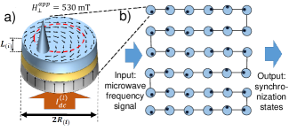
Spin-torque nano-oscillators Kiselev et al. (2003); Rippard et al. (2004) are nanoscale magnetic tunnel junctions composed of two ferromagnetic layers separated by a thin non-magnetic layer (Fig. 1a). They have the same structure as the actual cells in magnetic non volatile memories, and can be fabricated in large numbers in microelectronic chips Chung et al. (2016). A current applied to these nanojunctions becomes spin polarized and applies a spin-transfer torque on the local magnetization Slonczewski (1996); Berger (1996). For current densities above a threshold, this torque can generate sustained oscillations of the free layer magnetization, which in turn are converted into microwave voltage oscillations through magnetoresistive effects. The frequency of the oscillations can be varied from hundreds of MHz to tens of GHz by changing the materials and the geometry of the junctions in order to select the modes of magnetization dynamics Bonetti et al. (2009). Interestingly with spin-torque oscillators, once the pillar is fabricated, the frequency can still be tuned by hundreds of percent by varying the applied direct current or the magnetic field Slavin and Tiberkevich (2009). Spin-torque nano-oscillators also respond to input microwave signals in a large frequency band around frequencies at which they oscillate. This response can take multiple forms. For example, spin-torque nano-oscillators generate direct voltages if the input is a microwave current with a frequency close to their own. This rectification is called spin-diode effect Miwa et al. (2013); S. Jenkins et al. (2015). Another response for spin-torque nano-oscillators in the auto-oscillation regime is the synchronization of their oscillations to input microwave signals on a frequency span called injection locking range that can reach several percent of their base frequency Rippard et al. (2005); Lebrun et al. (2015).
We can therefore envision using arrays of spin-torque nano-oscillators with different base frequencies to analyze or process microwave signals on wide frequency bands from MHz to GHz Ebels et al. (2017); Louis et al. (2017) (Fig. 1b). The advantages of these circuits compared to standard spectral analysis techniques are the speed of processing, naturally performed in parallel, and the small dimensions of the arrays, based on nanoscale components with native sensitivity to microwaves and demonstrated CMOS compatibility. For example, in prior work, a small hardware array of four nano-oscillators has been built and used as a neural network for classifying microwave inputs in a range of a few tens of MHz Romera et al. (2018). In order to scale these experiments to practical applications, this frequency band needs to be adapted. For some applications, depending on the input to analyze, this frequency band will need to be increased to hundreds of MHz or more. For other applications it will be on the contrary more important to increase the frequency sensitivity than the covered frequency band. In both cases, this can be achieved by increasing the number of oscillators in the array and carefully choosing their properties.
The fabrication of such arrays is a major challenge towards many envisaged applications based on spin-torque nano-oscillators, but their design has never been investigated. It requires finely tuning the base frequency of the oscillators and the bandwidth of their response which both depend in different ways on the same parameters: injected direct current and geometry of the pillars. Furthermore, it is important to check that the mutual coupling between oscillators, which naturally arises when they are electrically connected or closely packed, does not compromise their individual response Awad et al. (2017); Lebrun et al. (2017); Locatelli et al. (2015). In this work, our focus is on oscillators with a vortex in the free layer as their properties are well described and understood Guslienko et al. (2006); Bortolotti et al. (2012); Grimaldi et al. (2014). We analytically derive design rules to build large arrays of uncoupled vortex spin-torque nano-oscillators with equally spaced frequencies and equal frequency sensitivity that can process microwave inputs on a wide frequency range. Here, by frequency sensitivity we refer to the frequency precision with which two microwave inputs can be distinguished by the array. Input microwave signals can be introduced either as ac magnetic fields (Romera et al. (2018) and this work) or as ac currents injected directly in the electrical circuit of the array Romera et al. (2016). We computed the optimal operating points (applied dc currents) and physical properties (size and aspect ratio) of the oscillators in the array. We show that arrays comprising hundreds of vortex oscillators with an overall response covering hundreds of MHz can be produced with existing nanofabrication techniques. We find that, counter-intuitively, arrays with the smaller number of oscillators will have the larger overall frequency band, but at the expense of a reduced frequency sensitivity. Finally we numerically simulate an array designed with these rules, taking into account the mutual coupling between oscillators. We show that for experimentally observed coupling values the whole array is functional and that the design rules derived analytically in the absence of coupling can be applied.
II Analytical expressions of the oscillator frequency and injection locking bandwidth
In order to design the arrays, the analytical expressions of the frequency and injection locking band of spin-torque nano-oscillators are first derived. As illustrated in Fig. 1a, spin-torque nano-oscillators with a vortex configuration in the free layer Metlov and Guslienko (2002) have a planar magnetization except in the vortex core area where it becomes out of plane. Here, we focus on spin-torque oscillators having a magnetic tunnel junction structure, however our approach can be extended to other magnetic structures. When a sufficient electrical current density is injected in the nano-pillar, the vortex core leaves its initial position in the free layer and starts to oscillate in a quasi-circular trajectory. By solving the Thiele equation Thiele (1973); Dussaux et al. (2012) describing the trajectory of the vortex core in the steady-state, the expression of the frequency of the vortex oscillations can be determined in Eq. (1) :
| (1) |
with the gyrovector magnitude, the magnetostatic confinement, Oersted field confinement, the nonlinear magnetostatic confinement, the nonlinear Oersted field confinement (see Appendix A) and the applied current density (, where is the junction radius and is the applied dc current) Dussaux et al. (2012). This frequency depends on the power of oscillations described by Eq. (2):
| (2) |
with the spin-transfer torque efficiency, the damping and its nonlinear factor Dussaux et al. (2012). The nonlinearity of the auto-oscillator is characterized by the nonlinear frequency shift Slavin and Tiberkevich (2009); Grimaldi et al. (2014) defined by Eq. (3):
| (3) |
This parameter combined with the power affects the frequency injection locking range on which the oscillator synchronizes to an external microwave signal of amplitude . The expression of the injection locking-range is given by Eq. (4) Slavin and Tiberkevich (2009).
| (4) |
The coefficients of these equations are described in Tables I and II. Their values depend on the magnetic material used as a free-layer. Here we chose to use parameters for free-layers made of FeB Tsunegi et al. (2014a) (Table I). Importantly, as can be seen in Table II, coefficients for the electrical current density , the damping , the confinement due to the Oersted field , the magnetostatic confinement and the gyroforce , depend on the free-layer radius , thickness , and applied dc current .
| mT (fixed perpendicular applied magnetic field) |
| (free layer magnetization)111 For free-layer thicknesses larger than 3 nm, variations smaller than 5% can be assumed. Therefore, for free-layer thicknesses used in this work (3.0 to 8.1 nm), for simplicity, a constant value was used. |
| (Gilbert damping)Tsunegi et al. (2014b) |
| (exchange constant) |
| (spin polarization) |
| (polarizer magnetization) |
| (nonlinear damping coefficient)Grimaldi et al. (2014); Khvalkovskiy et al. (2010) |
| (free layer magnetization angle) |
| (vortex core radius) |
| (spin-transfer torque efficiency) |
| (damping)Dussaux et al. (2012) |
| (gyrovector magnitude) |
| (magnetostatic coefficient)Guslienko et al. (2006); Gaididei et al. (2010) |
| (nonlinear magnetostatic coefficient)Gaididei et al. (2010) |
| (Oersted field confinement)Khvalkovskiy et al. (2010) |
| (nonlinear Oersted field confinement)Khvalkovskiy et al. (2010) |
III Tuning individual oscillator parameters for building large arrays: design rules.
In this section, the analytical model presented in the previous section is used to design an array of spin-torque nano-oscillators that can process microwave signals. This is achieved through their synchronization to the input microwave signals that they receive. Ideally, this microwave processing should be done on a wide range of input frequencies, with uniform sensitivity to all frequencies, and without any input frequency gap intervals where the nano-oscillator array will not be able to respond. These conditions allowed reaching the highest performance on a pattern classification task in experiments and in simulations for a small neural network of four spin-torque nano-oscillators Romera et al. (2018). In order to reach this particular regime, by tuning the individual properties of each nano-oscillator, we design an array where the individual frequency of oscillators are regularly spaced, and where each oscillator has a synchronization bandwidth to the external input (injection locking range) equal to this spacing. To do this, the frequency and the injection locking range of all spin-torque nano-oscillators of the array need to be tuned to fulfill the following two conditions:
| (5) |
and are respectively the maximum frequency and injection locking range deviations that we tolerate in the choice of our individual parameters, here chosen as 5% of the frequency spacing value (). In our approach, and are fixed value constraints for which Eq. (5) should be satisfied. Beyond knowing if such constraints can be satisfied or not, those are simply the initial specification of the array we would like to design. From Table II combined with Eq. (1) and (4) we see that the frequency and the injection locking range of each oscillator can be tuned through three parameters: the free-layer radius, its thickness and the applied dc current . We chose to separate the individual frequencies with a frequency step of 5 MHz, which corresponds to the typical measured locking ranges for this type of oscillators Romera et al. (2018). In order to take into account the reachable size accuracy of the nano-dot manufacturing processes, we also impose a minimum dot radius variation between nano-oscillators of nm and a minimum free layer thickness variation of 1 nm from one nano-dot to another . These minimum free-layer thickness and radius variations can also be seen as statistical mean indicators that capture the size deviation from nominal realization of the oscillators in the array. In our case, these parameters are given and are part of the initial design problem. Their value will depend on the presence of defects or fabrication imperfections. In this sense they are independent of the specific frequency sensitivity we want to achieve in the array. In order to reach self-sustained oscillations, for given lateral area () a sufficient electrical current density needs to be applied. Assuming a constant resistance-area product , the static Joule heating in the device will scale linearly with the lateral area: . Therefore, to avoid large Joule heating due to this area contribution, we consider a maximum nano-dot radius size of 300 nm. Furthermore, the maximum and minimum nano-pillar radius (300 and 150 nm) and thickness (8.1 and 3.0 nm) are chosen in such a way that the magnetic ground state of the FeB layer is always a vortex state.
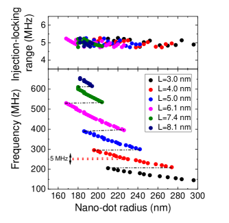
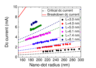
The applied dc currents are chosen according to the accuracy of the electrical circuit supplying them. Therefore, we impose a minimum current variation of mA from one oscillator to another one: . The applied dc current (as radius and thickness ) is considered as a parameter that allows tuning the individual frequency and injection locking range of the spin-torque oscillator. Its value is maintained constant in time during the microwave information processing. While the constant dc current is applied, all the oscillators of the array are in a self-sustained oscillatory regime. During this stage, the oscillator array receives a collection of magnetic microwave inputs (these inputs can be also encoded as electrical microwave inputs). Depending on the frequency mismatch between the oscillator and the input signal, some spin-torque nano-oscillators in the array can synchronize their oscillations to the input. Figs. 2 and 3 show the calculated values of free-layer radius, thickness and applied dc current that fill these constraints as well as conditions (i) and (ii) for an array of 100 oscillators. In order to find these values, we explore the three-dimensional space composed by . We defined a grid of points belonging to this finite size space where each point is separated from another by , and . At each point of this grid, we compute the frequency and the injection locking range (using Eq. (1,4)). If the computed frequency and injection locking range satisfy the aforementioned conditions of Eq. (5), then the corresponding parameters at that point are selected to be the parameters of the -th oscillator of the array we are designing. If a set of value gives rise to a frequency and injection-locking range that do not satisfy Eq. (5), this set is excluded and not used to build our array of oscillators. Therefore, for all the arrays presented in this work, all the oscillators verify the condition set by Eq. (5). This restriction can result in a reduction of the number of oscillators that we can have in the array.
In all panels of Figs. 2 and 3, each dot corresponds to one of the 100 oscillators of the array. The bottom panel of Fig. 2 shows the auto-oscillation frequencies of the oscillators as a function of their radius . The corresponding thicknesses are represented in different colors. The resulting frequencies cover a microwave range of 510 MHz starting from 145 MHz and ending at 655 MHz. For the considered range of current, the nonlinear frequency shift defined in Eq. (3) is comprised between 9 and 11 which is consistent with values found in the literature Grimaldi et al. (2014). For vortex-based spin-torque oscillator, the nonlinear frequency shift typically decreases as a function of the applied dc current in the self-sustained regime. If it is too small (respectively too large), the injection locking range become smaller (respectively bigger) too, and therefore the condition (ii) of Eq. (5) is not satisfied. Therefore, the nonlinear frequency shift needs to have an intermediate value. values used here correspond to an intermediate value regime that leads to injection locking ranges around 5 MHz. The top panel of Fig. 2 shows the corresponding injection locking ranges of each nano-oscillator. The distribution of this injection locking range is narrow around 5 MHz, which means, as desired, that each nano-oscillator of the array has a similar sensitivity to the external inputs that it receives. In Fig. 3, the dc currents applied to each individual oscillator are shown. Those applied dc currents are higher than the critical dc current (dashed lines) required to obtain auto-oscillations. This highlights the fact that all the nano-oscillators are in an auto-oscillation regime. In addition, the applied dc current is always set smaller than the breakdown current (red straight line) which should not be reached otherwise the magnetic junction would be damaged. Indeed, for bias voltages close or higher than 450 mV, a sudden degradation of tunneling properties is often observed experimentally. Thus, for a given resistance-area product, one can derive the corresponding breakdown current versus nano-pillar radius evolution we used here (see Appendix B).
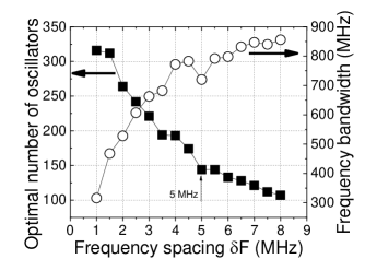
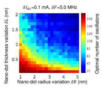
We now explore the conditions to obtain larger arrays () using Eq. (1,2,4), while insuring frequency and synchronization requirements (i) and (ii). Importantly, those conditions were examined for constraints given by the minimum variations of the free-layer size () and applied dc current I. In Fig. 4, we vary the frequency spacing between the individual oscillator frequencies from 1.0 to 8.0 MHz. This frequency spacing sets the sensitivity of the array to microwave inputs. For each value of frequency spacing, we computed the optimal number of oscillators in the array (black squares in Fig. 4) that gives rise to the largest frequency bandwidth over which the array will respond (white circles in Fig. 4). Here by array response we mean that at least one oscillator of the array will leave its free-running oscillation frequency and synchronize its oscillation to the frequency of the input frequency that was sent to the array. For a higher or lower input frequency, a different oscillator of the array should react. As for the design of the 100-oscillator array, here we explore the finite parameter space using a three-dimensional grid where each point is regularly separated by , and . Among these grid points, a proportion of them will satisfy frequency and synchronization bandwidth conditions (i) and (ii). These points are selected to be the parameters of the individual oscillators of the array we design. For a given frequency spacing, the total number of these distinct oscillators corresponds to the optimal number of oscillators than can be found. The observed optimal number of oscillator trends in Fig. 4 can be understood as follows. When the frequency spacing is large, multiple oscillators will satisfy these conditions despite the constraints, here set to nm, nm and mA. Therefore, for the larger frequency spacing of 8 MHz, the frequency bandwidth of the array (810 MHz) is practically equal to the frequency range accessible to vortex oscillators (850 MHz), limited only by the vortex ground state stability and the maximum current that can be sustained. The optimal number of oscillators in the array, 110, is then close to the frequency range achievable by vortex oscillators (850 MHz), divided by the frequency gap between oscillators (8 MHz). The situation is different when the frequency spacing between oscillators decreases. Then, due to the precision of lithography and injected current, it becomes more and more difficult to find oscillators with the required frequencies. For a frequency spacing of 1 MHz, the optimal number of oscillators in the array, 330, is much lower than the value that could be achieved without constraints ( close to 800). For this reason, as the array sensitivity increases (smaller ), the frequency bandwidth of the array decreases down to 300 MHz. The number of oscillators shown in Fig. 4 is the optimal array size. If the number of oscillators is smaller, the overall array bandwidth decreases. If the number of oscillators is higher, the required sensitivity is not achieved. To have a larger frequency bandwidth for a given , smaller minimum variations compared to the one chosen here are required. Fig. 5 shows the calculated optimum number of nano-oscillators in the array with the following dc current and frequency constraints: mA and MHz. The red region corresponding to arrays larger than one hundred nano-oscillators are obtained for conditions where the allowed minimal variation on radius and thickness are the smallest ones ( nm and nm). The blue region corresponding to arrays smaller than forty nano-oscillators can be achieved for less severe constraints where minimal variation on radius and thickness are allowed to be larger ( nm and nm).
IV Numerical study of a large spin-torque nano-oscillator array in presence of mutual electrical interaction
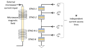
This section considers the impact of mutual interaction between oscillators. The largest arrays are obtained for the smallest frequency spacing, for which spin-torque nano-oscillators are more coupled if they interact. Electrical connections between oscillators for instance can lead to high mutual interactions when the frequency difference becomes small, of the order of 1 MHz for the oscillators modeled here Tsunegi et al. (2014a); Lebrun et al. (2017); Romera et al. (2018). This modifies their oscillation frequency and can lead to their mutual synchronization which can affect their ability to be synchronized to an external microwave input Romera et al. (2016). Here, the coupling phenomena is due to the sum of the rf emissions of the individual oscillators. In our case, where we consider N oscillators in series (see Fig. S1), every individual emission is shared through the whole electrical line. Therefore, every oscillator sees the same sum of total individual electrical microwave emissions. In this sense, all the rf emissions guided by serial electrical connections give rise to a global all-to-all coupling Georges et al. (2008). This collective coupling effect is not captured by the analytical description that we considered until now. We now examine the impact of oscillator mutual couplings on the array behavior through numerical simulations. For this purpose, we first study the collective behavior of an array of 100 electrically coupled spin-torque nano-oscillators that receives the sum of two distinct external microwave magnetic fields. This approach for applying microwave inputs to spin-torque nano-oscillators was used in experiments and simulations for an array of four coupled spin-torque nano-oscillators Romera et al. (2018). The parameters of all nano-oscillators in the array are the ones determined and displayed in Fig. 2 and 3. The electrical coupling between nano-oscillators resulting from their microwave emissions is described as an additional common alternating current that goes through all nano-oscillators Georges et al. (2008)
| (6) |
Here is the mean resistance variation due to the vortex core gyrotropic motion and tunnel magnetoresistance, is the load impedance which is equal to 50 , is the resistance of the junctions and Guslienko et al. (2002). In order to obtain the magnetization dynamics of the nano-oscillators, we numerically implement a fourth order Runge-Kutta scheme and solve the coupled differential Thiele equations (7)
| (7) |
simultaneously for the 100 vortex . Here, is the vortex core position, is the gyrovector, is the damping, is the potential energy of the vortex, is the spin-transfer force. The same numerical framework including the mutual electrical coupling has been shown previously to reproduce quantitatively the synchronization state features observed experimentally for an array of two Romera et al. (2016) and four Romera et al. (2018) coupled nano-oscillators in presence of external microwave stimuli.
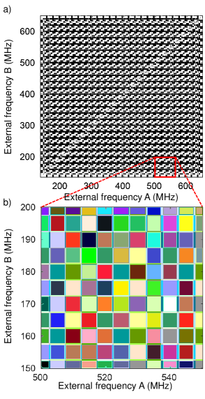
Fig. 6a shows the large variety of synchronization states obtained when two distinct external microwave stimuli with frequencies are injected to the array of one hundred spin-torque nano-oscillators. By sweeping the frequency of these external stimuli in the frequency range covered by the nano-oscillator array from 145 MHz to 655 MHz, each nano-oscillator is in turn synchronized around its free-running auto-oscillation frequency then desynchronized from the external signal. Each square corresponds to one unique synchronization state. The color of squares are chosen arbitrarily to help to distinguish between synchronization states neighbors. In this configuration, 9900 different synchronization states can be reached (by comparison, previous experimental work with four coupled nano-oscillators showed only 20 synchronization states Romera et al. (2018)). As shown in the synchronization map of Fig. 6a and corresponding zoom in Fig. 6b, the individual injection locking ranges and the frequency gap between closest nano-oscillator frequencies are very similar and, as designed, have a frequency size deviation smaller than 5%. This deviation from the desired frequency features ((i) and (ii)) varies with the collective electrical coupling conditions.
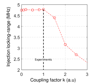
To highlight this effect, we study a smaller array of 10 coupled spin-torque nano-oscillators in presence of two injected microwave signals and simulate the system as it was done for the array of 100 nano-oscillators, for different amplitudes of the electrical coupling. To simulate distinct electrical coupling environments, we multiply the common emitted microwave current generated by all spin-torque nano-oscillators by a factor that allows tuning the strength of coupling in simulations. Thus we consider the following new common microwave current . corresponds to standard experimental conditions, while corresponds to an uncoupled oscillator array. For the coupling tuning values used here, different initial positions of the vortex core give rise to the same final frequency in the steady state oscillatory regime. As shown in Fig. 7, when the mutual coupling between oscillators increases, it strongly modifies the ability of the oscillators to phase lock to external microwave signals. For high coupling regimes corresponding to , the synchronization response of the array drastically decreases from the initially designed one. For such strong electrical coupling conditions, the spin-torque nano-oscillator array will not be sensitive to all the range of input frequencies it was designed for. For standard experimental coupling conditions corresponding to , the observed injection locking range does not decrease, and the array functions remain as desired. This numerical result shows that the analytical approach to designing large size arrays that we propose is robust to electrical coupling effects.
V Conclusion
Our analytical study shows that the properties of the free layer of spin-torque nano-oscillators as well as the amplitude of the injected dc current can be tuned to design arrays of oscillators responding to wide input frequency bandwidths of several hundreds of MHz. The technological constraints on junction dimensions and injected current, due to nano-processing and electrical circuit design, impose the optimal size of spin-torque nano-oscillator arrays for a given frequency sensitivity. We have shown that the maximum size of an optimal array is around 300 spin-torque nano-oscillators for realistic manufacturing parameters and vortex free-layer configuration. Finally, we have shown numerically that the mutual coupling between oscillators does not decrease the array performance as long as coupling remains moderate, close to the experimental values measured for electrical couplings.
Increasing the overall frequency response from hundreds of MHz to several GHz can be achieved by working with higher frequency junctions than vortex oscillators, for example using oscillators based on uniform magnetization dynamics Bonetti et al. (2009). The design rules and methods developed here can be easily extended to other types of spin-torque nano-oscillators. The equations for the dynamics of vortex oscillators are indeed identical to the formalism describing spin-torque nano-oscillators in general Slavin and Tiberkevich (2009); Grimaldi et al. (2014). Beyond magnetic tunnel junction structures, our design approach can be adapted to a novel variety of spintronic devices emerging from the recent spin-orbit torque advances Cai et al. (2017); Li et al. (2019). Moreover our work can also straightforwardly be extended to uneven frequency spacing between oscillators, following for example a logarithmic scale.
In summary, we have shown through simulations the possibility to build a device made of a large array of electrically coupled spin-torque nano-oscillators able to respond to microwave signals with a wide range of input frequencies with a constant sensitivity in the whole operating bandwidth. These results open the path to using such arrays in applications such as spectral analysis, microwave sensing and brain-inspired computing.
Acknowledgements
This work was supported by the European Research Council ERC under Grant bioSPINspired 682955. F.A.A. is a Research Fellow of the F.R.S.-FNRS.
Appendix A Oersted field and magnetostatic field contributions
The Oersted field (due to the perpendicular flow of electrical charge current J) modifies the energy landscape seen by the magnetic vortex core in the free-layer. For a given vortex core position , this additional energy contribution is captured by a Zeeman energy term, formed by the interaction between the local Oersted field and the local magnetization , averaged over the whole magnetic volume of the free-layer. Here corresponds to the position of the local magnetization. For a given vortex magnetization profile, this energy term was calculated and approximated by a polynomial expression S_RefA ; Khvalkovskiy et al. (2010).
| (8) |
In this expression, the linear Oersted field confinement coefficient corresponds simply to a scaling factor of the term in (respectively the nonlinear Oersted field confinement coefficient scales the term in ). Here is the nano-pillar radius of the free-layer.
Similarly, for a given vortex core position , one can derive the Zeeman interaction energy term due to the demagnetization field . This demagnetization field is due to spatial magnetic charges caused by the intrinsic magnetization distribution in the free-layer than can appear in the absence of an applied bias. For a given vortex magnetization profile, Gaidedei et al. Gaididei et al. (2010) calculated this energy term which is approximated through the following polynomial expression:
| (9) |
In this expression, the linear magnetostatic confinement coefficient corresponds to a scaling factor of the term in (respectively the nonlinear magnetostatic confinement coefficient scales the term in ).
Appendix B Breakdown current
For a given resistance-area product , the following expression defines the breakdown current as a function of the nano-pillar radius :
| (10) |
Here, mV, is chosen to be similar to the FeB based (free-layer) spin-torque oscillators used experimentally in our experimental work of Romera et al. (2018). The evolution of this breakdown current is plotted in Fig. 3.
Appendix C Electrical circuit of the studied spin-torque nano-oscillator array
References
- Kiselev et al. (2003) S. I. Kiselev, J. C. Sankey, I. N. Krivorotov, N. C. Emley, R. J. Schoelkopf, R. A. Buhrman, and D. C. Ralph, Nature 425, 380 (2003).
- Rippard et al. (2004) W. H. Rippard, M. R. Pufall, S. Kaka, S. E. Russek, and T. J. Silva, Physical Review Letters 92, 027201 (2004).
- Chung et al. (2016) S.-W. Chung, T. Kishi, J. W. Park, M. Yoshikawa, K. S. Park, T. Nagase, K. Sunouchi, H. Kanaya, G. C. Kim, K. Noma, M. S. Lee, A. Yamamoto, K. M. Rho, K. Tsuchida, S. J. Chung, J. Y. Yi, H. S. Kim, Y. Chun, H. Oyamatsu, and S. J. Hong (2016) pp. 27.1.1–27.1.4.
- Slonczewski (1996) J. C. Slonczewski, Journal of Magnetism and Magnetic Materials 159, L1 (1996).
- Berger (1996) L. Berger, Physical Review B 54, 9353 (1996).
- Bonetti et al. (2009) S. Bonetti, P. Muduli, F. Mancoff, and J. Ã…kerman, Applied Physics Letters 94, 102507 (2009).
- Slavin and Tiberkevich (2009) A. Slavin and V. Tiberkevich, IEEE Transactions on Magnetics 45, 1875 (2009).
- Miwa et al. (2013) S. Miwa, S. Ishibashi, H. Tomita, T. Nozaki, E. Tamura, K. Ando, N. Mizuochi, T. Saruya, H. Kubota, K. Yakushiji, T. Taniguchi, H. Imamura, A. Fukushima, S. Yuasa, and Y. Suzuki, Nature materials 13 (2013), 10.1038/nmat3778.
- S. Jenkins et al. (2015) A. S. Jenkins, R. Lebrun, E. Grimaldi, S. Tsunegi, P. Bortolotti, H. Kubota, K. Yakushiji, A. Fukushima, G. de Loubens, O. Klein, S. Yuasa, and V. Cros, Nature nanotechnology 11 (2015), 10.1038/nnano.2015.295.
- Rippard et al. (2005) W. H. Rippard, M. R. Pufall, S. Kaka, T. J. Silva, S. E. Russek, and J. A. Katine, Physical review letters 95, 067203 (2005).
- Lebrun et al. (2015) R. Lebrun, A. Jenkins, A. Dussaux, N. Locatelli, S. Tsunegi, E. Grimaldi, H. Kubota, P. Bortolotti, K. Yakushiji, J. Grollier, A. Fukushima, S. Yuasa, and V. Cros, Physical review letters 115 (2015), 10.1103/PhysRevLett.115.017201.
- Ebels et al. (2017) U. Ebels, J. Hem, A. Purbawati, A. R. Calafora, C. Murapaka, L. Vila, K. J. Merazzo, E. Jimenez, M. Cyrille, R. Ferreira, M. Kreissig, R. Ma, F. Ellinger, R. Lebrun, S. Wittrock, V. Cros, and P. Bortolotti, in 2017 Joint Conference of the European Frequency and Time Forum and IEEE International Frequency Control Symposium (EFTF/IFCS) (2017) pp. 66–67.
- Louis et al. (2017) S. Louis, V. Tyberkevych, J. Li, I. Lisenkov, R. Khymyn, E. Bankowski, T. Meitzler, I. Krivorotov, and A. Slavin, IEEE Transactions on Magnetics 53, 1 (2017).
- Romera et al. (2018) M. Romera, P. Talatchian, S. Tsunegi, F. Abreu Araujo, V. Cros, P. Bortolotti, J. Trastoy, K. Yakushiji, A. Fukushima, H. Kubota, S. Yuasa, M. Ernoult, D. Vodenicarevic, T. Hirtzlin, N. Locatelli, D. Querlioz, and J. Grollier, Nature 563 (2018), 10.1038/s41586-018-0632-y.
- Awad et al. (2017) A. Awad, P. Dürrenfeld, A. Houshang, M. Dvornik, E. Iacocca, R. Dumas, and J. Åkerman, Nature Physics 13, 292 (2017).
- Lebrun et al. (2017) R. Lebrun, S. Tsunegi, P. Bortolotti, H. Kubota, A. Jenkins, M. Romera, K. Yakushiji, A. Fukushima, J. Grollier, S. Yuasa, et al., Nature communications 8, 15825 (2017).
- Locatelli et al. (2015) N. Locatelli, A. Hamadeh, F. Abreu Araujo, A. D. Belanovsky, P. N. Skirdkov, R. Lebrun, V. V. Naletov, K. A. Zvezdin, M. Muñoz, J. Grollier, O. Klein, V. Cros, and G. de Loubens, Scientific Reports 5, 17039 (2015).
- Guslienko et al. (2006) K. Y. Guslienko, X. F. Han, D. J. Keavney, R. Divan, and S. D. Bader, Physical Review Letters 96, 067205 (2006).
- Bortolotti et al. (2012) P. Bortolotti, A. Dussaux, J. Grollier, V. Cros, A. Fukushima, H. Kubota, K. Yakushiji, S. Yuasa, K. Ando, and A. Fert, Applied Physics Letters 100, 042408 (2012).
- Grimaldi et al. (2014) E. Grimaldi, A. Dussaux, P. Bortolotti, J. Grollier, G. Pillet, A. Fukushima, H. Kubota, K. Yakushiji, S. Yuasa, and V. Cros, Physical Review B 89, 104404 (2014).
- Metlov and Guslienko (2002) K. L. Metlov and K. Y. Guslienko, Journal of magnetism and magnetic materials 242, 1015 (2002).
- Thiele (1973) A. A. Thiele, Physical Review Letters 30, 230 (1973).
- Dussaux et al. (2012) A. Dussaux, A. V. Khvalkovskiy, P. Bortolotti, J. Grollier, V. Cros, and A. Fert, Physical Review B 86, 014402 (2012).
- Tsunegi et al. (2014a) S. Tsunegi, H. Kubota, K. Yakushiji, M. Konoto, S. Tamaru, A. Fukushima, H. Arai, H. Imamura, E. Grimaldi, R. Lebrun, et al., Applied Physics Express 7, 063009 (2014a).
- Tsunegi et al. (2014b) S. Tsunegi, H. Kubota, S. Tamaru, K. Yakushiji, M. Konoto, A. Fukushima, T. Taniguchi, H. Arai, H. Imamura, and S. Yuasa, Applied Physics Express 7, 033004 (2014b).
- Khvalkovskiy et al. (2010) A. V. Khvalkovskiy, J. Grollier, N. Locatelli, Y. V. Gorbunov, K. A. Zvezdin, and V. Cros, Applied Physics Letters 96, 212507 (2010).
- Gaididei et al. (2010) Y. Gaididei, V. Kravchuk, and D. Sheka, International Journal of Quantum Chemistry 110, 83 (2010).
- Romera et al. (2016) M. Romera, P. Talatchian, R. Lebrun, K. Merazzo, P. Bortolotti, L. Vila, J. Costa, R. Ferreira, P. Freitas, M. C. Cyrille, U. Ebels, V. Cros, and J. Grollier, Applied Physics Letters 109 (2016), 10.1063/1.4972346.
- Georges et al. (2008) B. Georges, J. Grollier, V. Cros, and A. Fert, Applied Physics Letters 92, 232504 (2008).
- Guslienko et al. (2002) K. Y. Guslienko, B. Ivanov, V. Novosad, Y. Otani, H. Shima, and K. Fukamichi, Journal of Applied Physics 91, 8037 (2002).
- Cai et al. (2017) K. Cai, M. Yang, H. Ju, S. Wang, Y. Ji, B. Li, K. W. Edmonds, Y. Sheng, B. Zhang, N. Zhang, et al., Nature materials 16, 712 (2017).
- Li et al. (2019) Y. Li, K. W. Edmonds, X. Liu, H. Zheng, and K. Wang, Advanced Quantum Technologies 2, 1800052 (2019).
- (33) Y-S. Choi, S-K. Kim, K-S. Lee, Y-S. Yu, Appl. Phys. Lett. 93, 182508 (2008)..