Observation of quantum corrections to conductivity up to optical frequencies
Abstract
It is well known that conductivity of disordered metals is suppressed in the limit of low frequencies and temperatures by quantum corrections. Although predicted by theory to exist up to much higher energies, such corrections have so far been experimentally proven only for 80 meV. Here, by a combination of transport and optical studies, we demonstrate that the quantum corrections are present in strongly disordered conductor MoC up to at least 4 eV, thereby extending the experimental window where such corrections were found by a factor of 50. The knowledge of both, the real and imaginary parts of conductivity, enables us to identify the microscopic parameters of the conduction electron fluid. We find that the conduction electron density of strongly disordered MoC is surprisingly high and we argue that this should be considered a generic property of metals on the verge of disorder-induced localization transition.
At finite frequencies , the optical conductivity of any material is a complex quantity, . In the limit of low frequencies, only the conduction band contributes to the real part of the optical conductivity of a metal; the complex conductivity of this band is customarily described by the Drude formulaZiman72 ; Scheffler05
| (1) |
where is the relaxation rate determined by the collision time of the electrons . Within the simplest model of free electrons the classical dc conductivity is given by , where is the electron concentration and is the electron mass.Ziman72
With increasing disorder strength, increases and decreases, until at some critical disorder level the (three-dimensional, 3D) metal turns into an insulator, as predicted long ago by Anderson.Anderson58 At that point vanishes in the limit of low temperatures and, if Eq. (1) were to apply, the optical conductivity would vanish identically for all . However, this is unphysical, since at nonzero frequencies the absorption has to be finite even in the insulating state. Therefore, in the insulating state, Eq. (1) can not be valid. Instead, the low-frequency conductivity has to grow with and, by continuity, the same behaviour has to be expected also on the metallic side of the metal-insulator transition.
It is in fact well known that, in weakly disordered 3D metals, the conductivity in the small- and limit can be described as , where is the regular part of the conductivity and is the quantum correction which grows with . Two mechanisms have been proposed for the latter: it can be either due to the so-called weak-localization corrections,Gorkov79 or due to interaction effects.Altshuler79 It is remarkable that, up to numerical prefactors, at both mechanisms yield the same functional form of the quantum correction.Altshuler85 Its real part, , can be written in a unified way as
| (2) |
The quantum correction is finite at and its magnitude is characterized by a dimensionless number , to be called quantumness. We emphasize that our parametrization Eq. (2) reflects the fact that the quantum correction has to diminish the conductivity.
Numerical simulations by Weisse within the weak-localization scenario at temperature have shown that, at not too high frequencies, Eq. (2) is qualitatively valid not only for weakly disordered metals, but in a broad range of disorder strengths in the metallic phase.Weisse04 Throughout the metallic phase, Weisse’s data indicate that is of the same order of magnitude as , where is the Fermi energy: in the limit of weak disorder this result is well known;Altshuler85 in the opposite limit when the metal-insulator transition is approached, the quantumness and is comparable with .note_weisse
In order to generalize the above formulae for to finite temperatures, we follow the recipes of Fermi liquid theory and replace by where is a temperature-dependent scattering rate which depends on the mechanism for the quantum corrections: in case of weak-localization corrections it is the phase-breaking scattering rate, whereas for interactions effects . Detailed calculationsAltshuler85 for weakly disordered metals do confirm such a procedure, again up to numerical prefactors.
Motivated by Weisse’s data and analytical theory for weakly disordered metals, we postulate (throughout the metallic phase) the following simple formula for the frequency- and temperature-dependence of the real part of the optical conductivity which features the Drude behaviour Eq. (1) in the high-frequency limit and, at the same time, for takes into account the 3D quantum correction Eq. (2):
| (3) | |||||
| (4) |
The model Eqs. (3,4) depends on three parameters: , , and . Once these are known, the magnitude of the crossover frequency follows from assuming that the function is continuous.methods We treat and as independent, while for we keep the classical expression .
The most comprehensive experimental test of the formula Eq. (3) has been performed on the amorphous Nb:Si system close to its metal-insulator transition.Lee00 For samples at the metallic side of the transition, very good agreement has been found with a slightly generalized version of Eq. (3) for temperatures K and at frequencies up to 1 THz, both corresponding to meV. However, there are two reasons to expect that in very dirty systems such as Nb:Si Eq. (3) actually applies in a much wider frequency range: First, close to the metal-insulator transition should be comparable with the bandwidth.Altshuler85 Second, the tunneling density of states in amorphous Nb:Si is reduced at least up to 200 meV from the Fermi level.Bishop85 This latter observation also suggests that the quantum correction to conductivity in amorphous Nb:Si is due to interaction effects.
The goal of the present paper is to look for quantum corrections to conductivity in a much broader frequency range and to check whether they can be observable even at optical frequencies. To this end, we have chosen to study the highly disordered conductor MoC,Lee90 ; Szabo2016 since in this material quantum corrections have been observed in transport measurements up to 300 K,Lee94 corresponding to meV.
The amount of disorder in MoC can be conveniently tuned by varying the Mo:C stoichiometry and/or by the film thickness: both, the reduction of film thickness and the increase of the carbon content, lead to an increase of the sheet resistance . In the present work, we study two sets of samples: in the first set, we prepared films with thickness =5 nm and varying Mo:C stoichiometry, while in the second set, we have studied films at fixed stoichiometry but with varying thickness. Details on preparation of the MoC films are in the supplementary material.methods
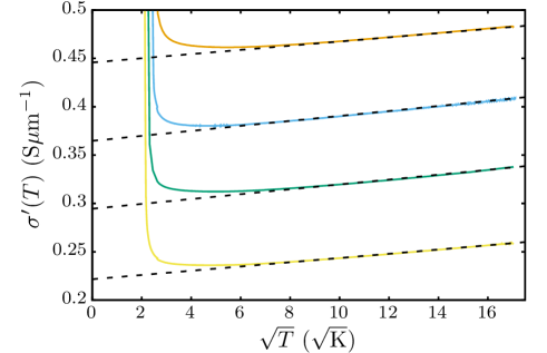
The temperature dependence of dc conductivity for the set of samples with fixed thickness is presented in Fig. 1. In a transport measurement and therefore . As can be seen, exhibits very good scaling with the square root of temperature from K up to room temperature, precisely as expected according to Eq. (3) in case of dominant interaction effects with . The deviations from this scaling below are caused by the superconducting transition and the associated fluctuation conductivity. Moreover, dimensional crossover between 3D and 2D quantum corrections is expected to occur at temperatures comparable with .methods
As can be seen from Fig. 1, the two terms in Eq. (3) exhibit quite different evolution with stoichiometry: the extrapolated value of the conductivity decreases when the metal-insulator transition is approached, whereas the coefficient in front of is roughly constant. Similar behaviour has been observed previously in Nb:SiBishop85 ; Lee00 and in TiOx;Vlekken91 it is also consistent with our model Eqs. (3,4).methods
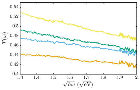
In Fig. 2 we show the optical transmission in a broad frequency range for the same set of films on sapphire substrates as in Fig. 1. The absence of any spectral features indicates that interband transitions are absent in this range, a point we will come to later. Similar featureless transmission data is also obtained for the set of films with varying thickness. This indicates that the details of microstructure are not important for the phenomena we observe and that, for both sets of samples, the crucial control parameter is the degree of disorder.methods
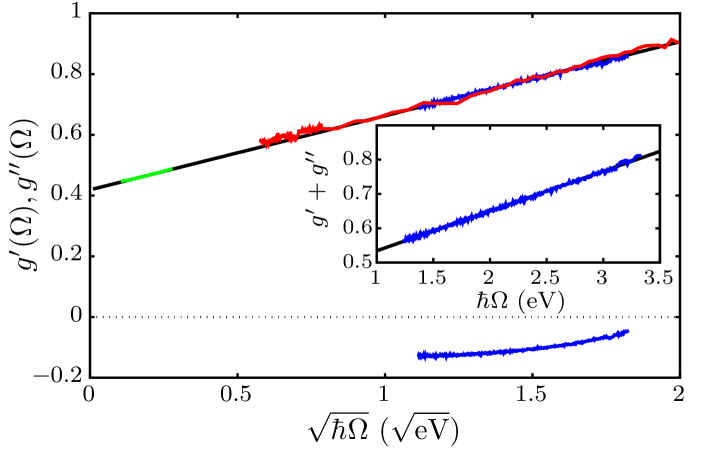
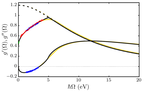
Assuming , the real part of the dimensionless sheet conductancenote_conductance of the MoC films , where is the impedance of free space, can be calculated from the transmission .methods The thus obtained conductance of a MoC film with thickness =5 nm and room temperature sheet resistance is shown in Fig. 3. Also shown in Fig. 3 is the ellipsometry data for both components of which is obtained in a somewhat more narrow frequency range. Since at optical frequencies , we do not have to distinguish between and . The temperature dependence of the conductivity for a sample from the same batch is replotted here from Fig. 1 as well, assuming . Note the very good agreement between all three data sets.
Since conductivity and dimensionless conductance differ only by a multiplicative constant, when talking about frequency- and temperature dependence, from now on we will use these terms interchangeably.
The data presented in Fig. 3 is the main result of this paper. It shows that the real part of conductivity of strongly disordered MoC thin films is very well described by Eq. (3) in a broad range of frequencies from meV up to at least eV. Although this is expected from the theoretical point of view since the scattering rate in dirty metals close to the metal-insulator transition is huge, to our knowledge, until now it has not been demonstrated experimentally. As a consequence, this fact is not generally adopted and it is often incorrectly assumed that quantum corrections are not present at room temperature or at optical frequencies.
Equally remarkable are the results for the imaginary part of conductivity which are also presented in Fig. 3. It should be pointed out that, unlike the real part of conductivity which is (in the studied frequency range) determined only by the contribution of the conduction band, there exists an additional contribution to from the bound electrons, where is the permittivity of vacuum and is the bound-electron contribution to the static dielectric constant. Thus the presence of a negative contribution to is by itself not surprising. However, the experimental data in Fig. 3 clearly indicate that is not linear in frequency. In fact, the data contain an anomalous term with the same magnitude and opposite sign as in the real part Eq. (3). Such a term is required to be present by the Kramers-Kronig relations and in the inset to Fig. 3 we demonstrate that, as was to be expected, the anomalous terms perfectly cancel in the sum .
The next natural question to ask is: what are the values of the parameters , , and which enter Eq. (3)? From Fig. 3 we have access to only two parameters: the value of the conductivity and the coefficient in front of . On the other hand, if we could extend our measurements to higher frequencies and measure the crossover scale predicted by Eqs. (3,4), this would give us the needed third data point. Unfortunately, at frequencies above eV the transmission of our sapphire substrates is influenced by impurity absorption and therefore we can not measure directly.
Nevertheless, one can approximately determine the complex conductivity in the whole frequency range from a measurement of both, and , in a finite interval of frequencies.Dienstfrey2001 The key observation is that the real and imaginary parts of conductivity have to satisfy the Kramers-Kronig relations, and therefore one can write down integral equations for the unknown conductivity outside the measured range. However, since such analytic continuation problem is ill-posed, additional simplifying assumptions have to be made. We have used the following procedure for the prolongation of the data, which turned out to be quite robust: We start by choosing a value of . Having made this choice, we can unambiguously find and from fitting the real part of conductivity to Eq. (3). With known , , and , the real part of conductivity is known from Eqs. (3,4) on the entire real axis. Next we calculate, making use of the Kramers-Kronig relations, the imaginary part of the conductivity . Finally we adjust the value of so that good agreement with of the conduction band is obtained. Note that in order to obtain the latter, the contribution of the bound electrons should be subtracted from the ellipsometric data for the imaginary part of conductivity in Fig. 3.
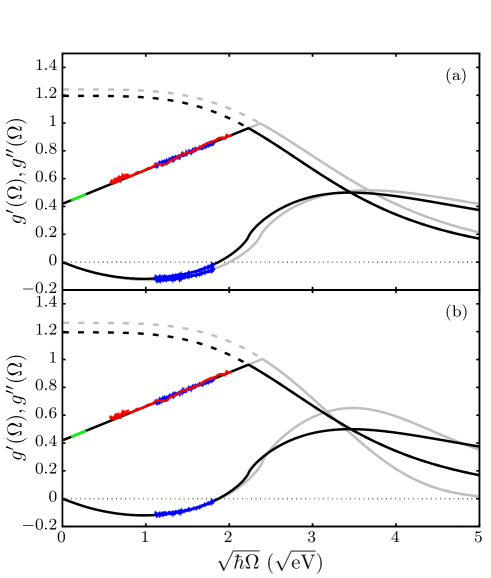
The results of the described prolongation procedure are presented in Fig. 4 and the corresponding fitting parameters are summarized in Table 1. One observes that all presented prolongations of fit the of the conduction band very well. The extracted values of the parameters , , and do depend on the assumed value of , but the variation between the results for and is at most 10 %. It can be shown that the most likely value of is bounded by these two values.methods
In order to further test the robustness of our prolongation procedure, we have modelled the real part of conductivity at high frequencies by the Gaussian formula instead of Eq. (4). As shown in Fig. 4, the resulting fits of are equally good as when Eq. (4) is used, and the scatter in the parameters , , and is at the level of 15 % or less. We have also checked that when the cusp at in the frequency dependence of is smoothened, the results of the prolongation procedure exhibit only marginal changes.methods Based on all of this evidence we conclude that our prolongation procedure is robust and the extracted parameters , , and are known with % uncertainty.
According to Table 1, the quantum corrections are appreciable, . Therefore the limit of the dc conductivity, , is reduced from the classical value roughly by a factor of 3. If one were to interpret the limit of the measured dc conductivity data of the studied sample as (as is frequently done), one would overestimate the scattering rate by the same factor of 3.
| Drude, Eq. (4) | Gaussian | |||
| 1.0 | 1.4 | 1.0 | 1.4 | |
| 1.25 | 1.20 | 1.32 | 1.26 | |
| 0.66 | 0.65 | 0.68 | 0.67 | |
| (eV) | 11.5 | 10.1 | 13.6 | 12.0 |
| ( cm-3) | 4.1 | 3.5 | 5.1 | 4.3 |
Regarding the energy scale , it is surprisingly large, eV. This does make sense, however: up to 4 eV, the real part of conductivity is described by Eq. (3) without any noticeable higher powers of frequency. This must mean that the crossover scale is by a wide margin larger than 4 eV. If one further observes that for we have ,methods the large value of seems to be inevitable.
What is even more surprising is that the electron concentration in the conduction band is very large, more than twice as large as in metallic aluminum. We believe that this is a consequence of the large value of : the individual electronic bands which are separated by energy less than lose their identity and merge together. In order to estimate the electron concentration predicted by such a picture, let us start by considering cubic MoC which crystallizes in the rocksalt structure with lattice constant 4.27 ÅKrasnenko12 and concentration of one type of atoms cm-3. The valence electron configurations of the Mo and C atoms are 4d5 5s1 and 2s2 2p2, respectively. According to band-structure calculations,Kavitha16 ; Krasnenko12 the relevant 4d and 5s states of molybdenum as well as the 2s and 2p states of carbon are within from the Fermi energy. Therefore it is reasonable to assume that the conduction electron fluid is formed by all 10 valence electrons and the corresponding electron density is cm-3, a value within the error bar of the data in Table 1. As a matter of fact, the value of in a highly disordered material is actually expected to be lower than the value for a perfect crystal which we have used; this (as well as an excess of carbon atoms which we also did not take into account) should decrease our estimate of and improve the agreement with Table 1. It is also worth pointing out that the absence of interband transitions up to 4 eV (see Fig. 2) provides an additional non-trivial consistency check of our proposal that the conduction electron “band” is very broad.
Because of the mechanism just described, we believe that the electron concentration in the conduction fluid of a dirty metal close to the metal-insulator transition should be (somewhat paradoxically) generically large. In fact, e.g. in dirty NbN samples large values of have already been observed: a naive analysis of the Hall coefficient at 20 K in films with resistivity cm yieldsDestraz17 cm-3. However, quantum corrections to the Hall coefficient are known to be present in similar samples of NbN,Chand09 and therefore the quoted value of should be taken as a lower bound to the actual electron concentration in the conduction fluid. NbN crystallizes in the rocksalt structure with lattice constant 4.39 ÅShiino10 and concentration of one type of atoms cm-3. It has the same electron count of 10 valence electrons as MoC, therefore within our picture we should expect cm-3, which is in reasonable agreement with the Hall estimate.
It is worth pointing out that the large values of electron concentration reported in Table 1 imply a large Fermi energy . In fact, making use of the free-electron estimate we find eV. Nevertheless, the customary parameter characterizing the disorder level, defined by , is quite small, , and this is consistent with the large quantumness .
In conclusion, we have demonstrated that, in strongly disordered metals on the verge of disorder-induced localization transition, quantum corrections to conductivity may be present up to optical frequencies. This effect should be universal; therefore quantum corrections should be added to the list of known reasonsScheffler05 why the canonical Drude formula for the frequency dependence of conductivity is hard to observe. We speculate that quantum corrections at infrared frequencies and above may already have been observed previously, but they were interpreted in a different way. Most notable candidates are liquid mercuryInagaki81 and perhaps also Si:P.Gaymann95 It therefore seems worthwhile to also take the quantum corrections into account in models used for spectroscopic ellipsometry.
We have likewise demonstrated how the combined knowledge of both, the real and imaginary parts of the optical conductivity, can be used to extract microscopic parameters of the conduction electron fluid in dirty metals which are not directly accessible otherwise - such as the quantumness , the scattering rate , and especially the electron concentration . We have found that is very large in MoC close to the metal-insulator transition; its value indicates that the conduction electron fluid is formed by all valence electrons. We have argued that the large value of should be a generic property of dirty metals, since individual electronic bands which are separated by energy less than lose their identity and merge together.
Supplementary material
MoC: sample preparation and characterization
The MoC thin films were prepared by means of reactive magnetron deposition from a Mo target in argon-acetylene atmosphere (both gases used of purity 5.0) on c-cut sapphire wafers heated to 200 degrees Celsius. The flow rate of argon was kept fixed, whereas the flow rate of acetylene was varied between depositions, in order to tune the Mo:C stoichiometry. During deposition, the magnetron current was held constant at 200 mA implying a deposition rate nm/min. The deposition time, and thus the thickness, was regulated by means of a programmable shutter control interface with precision of 1 s. The chamber was evacuated to approximately Pa. More details on preparation of the MoC films and their characterization have been published before.Trgala14
STM and STS measurements show that films with a thickness larger than 3 nm are spatially homogeneous, with typical rms roughness of 0.6 nm.Szabo2016
Two sets of samples were studied: in the first set, we prepared films with a constant thickness nm and the Mo:C stoichiometry was changed by varying the flow rate of acetylene. The sheet resistances of the samples at room temperature were , 500, 590, and, 720 .
In the second set, the stoichiometry was kept fixed at a value which maximizes the superconducting for films with 30 nm thickness. We have prepared samples with thickness , 15, 10, and 5 nm with sheet resistances , 120, 216, and 495 , respectively.
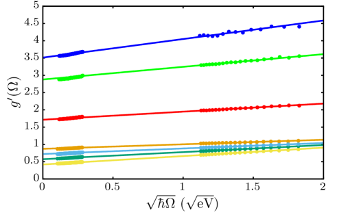
In Fig. 5 we show the normalized sheet conductance for both sets of MoC thin films. The plotted data is obtained from the temperature dependence of the dc conductivity and from ellipsometry in the same way as in Fig. 3. Good scaling with is found for all samples. The larger sample-to-sample variations in the second set are a trivial consequence of the varying sample thickness.
Optical measurements
The frequency dependence of the real and imaginary part of sheet conductance was measured by spectroscopic ellipsometryHumlicek05 at room temperature in the wavelength range 370 to 1000 nm using a rotating - compensator instrument J. A. Woollam, M-2000V.
The transmission measurements were performed at normal incidence of light to the sample surface. In the visible and ultraviolet frequency range we have used the UV VIS Carl Zeiss spectrometer and the Ocean Optics spectrometer (USB650UV). The transmission spectra in infrared up to 2.5 m were obtained by using the SPM2 Carl Zeiss grating monochromator (gratings No456039 and No465645) with Hamamatsu K1713-01 Si photodiode and PbS cell. At larger wavelengths up to 6 m, a modified UR20 Carl Zeiss IR spectrometer with a LiF prism was used.
The real part of the normalized sheet conductance was extracted from the transmission data as follows. Let us consider transmission of light (at normal incidence) across a thin film with complex normalized sheet conductance and thickness which is deposited on a thick dielectric substrate (in our case the substrate thickness is m) with a purely real index of refraction . Let the transmission of light from vacuum across the thin film into the substrate be and let the corresponding reflection be . The transmission and reflection through the interface substrate-vacuum are given by and , respectively, and the total transmission through the system ’film + substrate’ is
If the thickness satisfies the constraints and , then we can approximately write
For we have used a three-term dispersion formulaMalitson62 according to which varies between 1.75 and 1.79 throughout the visible range. Assuming furthermore that (see Fig. 3) one can show that and therefore the measured transmission is given by
When analyzing the experimental data, we have neglected the term in the denominator. Comparing with Fig. 3 one can check a posteriori that this procedure is justified.
Notes on the model Eqs. (3,4)
The crossover frequency of the model Eqs. (3,4) is given by with a -dependent prefactor, . The function is monotonic in the whole interval between 0 and 1. In the limit of weak quantum corrections, , it reduces to . This is consistent with the expectation that should vanish when . In the limit of strong quantum corrections and the crossover frequency is a substantial fraction of , again in agreement with expectations.
Weisse’s data indicate that stays finite when the metal-insulator transition is approached,Weisse04 i.e. for , and from here it follows that also stays finite in this limit, as claimed in the main text. Consequently, close to the metal-insulator transition, the prefactor of the term in Eq. (3) varies only weakly with the disorder strength, whereas the frequency-independent term drops to zero as the transition is approached.
Estimate of the dielectric constant
By definition, , where is the interband conductivity.note_epsilon Making use of the Kramers-Kronig relations we thus find
where in the approximate equality we have modelled the interband conductivity by a set of oscillators with frequency and oscillator weights . From the f-sum rule we know that , where is the total electron density in the material and is the oscillator weight of the conduction electrons.
As a rough estimate we will assume that, when the effect of a large is taken into account, the spectrum of the material consists of deep atomic-like electron levels labelled by , and of a single conduction band extending to infinity. In such case all interband transitions take place between and the conduction band, so that we can label them as . Moreover, we will assume that where is the number of electrons in the atomic level , whereby we approximately satisfy the f-sum rule. Thus we arrive at the following estimate of :
| (5) |
where (as an upper bound on ), for we take the distance between the Fermi level and the atomic level .
As a test of our estimate, let us calculate of metallic aluminum.note_aluminum In this case we take the 3s and 3p levels as those forming the conduction band, whereas there are 3 core levels (1s, 2s, and 2p) with , , and and excitation energies eV, eV, and eV.Williams For an fcc crystal with lattice constant Å, we obtain eV2, and therefore , which compares reasonably with the result of a much more detailed study.Smith78
Turning to MoC, we have eV2. The relevant (not too low-lying) core orbitals for molybdenum are 4p, 4s, and 3d with equal to 6, 2, and 10, respectively. The corresponding energies are equal to 36 eV, 63 eV, and 228 eV, respectively.Williams For carbon, there exists only one core orbital 1s with and eV.Williams With these values, we find .
Robustness of the prolongation procedure
Instead of the model Eqs. (3,4) which exhibits a cusp, let us consider the following function with the same low- and high-frequency functional forms, which in addition contains an intermediate frequency region from to that smoothly connects the low- and high-frequency formulae:
where and is a dimensionless frequency. In order to proceed, we have to fix the frequency where the real part of the conductivity starts to deviate from Eq. (3).
The prolongation procedure proceeds as follows. We start by guessing the frequency scale and, with known , we determine and from a fit of the measured data to Eq. (3). The 5 remaing parameters and are determined by requiring that the function and its first derivative are continuous at and ; furthermore we require that . Having specified the real part of conductivity , the rest of the prolongation procedure is the same as described in the main text: we iterate the choice of until the Kramers-Kronig image of reproduces the required .
| (eV) | 3.3 | 4.1 | 5.0 |
|---|---|---|---|
| 1.20 | 1.20 | 1.20 | |
| 0.65 | 0.65 | 0.65 | |
| (eV) | 10.4 | 10.2 | 10.1 |
Estimate of the 3D/2D crossover temperature
If interaction effects dominate the quantum correction, the crossover from 3D to 2D behaviour in a film of thickness is expected to occur close to the temperature where is the diffusion coefficient. Expressing in terms of the mean free path we can write
For a film with thickness nm, making use of we then obtain meV which corresponds to a crossover temperature K.
Acknowledgements.
We thank P. Markoš and M. Moško for useful discussions and A. Weisse for sending us his numerical data. This work was supported by the Slovak Research and Development Agency under the contract APVV-16-0372. R.H. was supported by the Slovak Research and Development Agency under Contract No. APVV-15-0496.References
- (1) J. M. Ziman, Principles of the Theory of Solids (Cambridge University Press, 1972).
- (2) M. Scheffler, M. Dressel, M. Jourdan, and H. Adrian, Nature 438, 1135 (2005).
- (3) P. W. Anderson, Phys. Rev. 109, 1492 (1958).
- (4) L. P. Gor’kov, A. I. Larkin, and D. E. Khmelnitskii, JETP Lett. 30, 228 (1979). The weak-localization corrections are due to the change of single-particle eigenstates and are present even in non-interacting systems of electrons.
- (5) B. L. Altshuler and A. G. Aronov, Solid State Commun. 30, 115 (1979). Interaction corrections are related to the change of the density of states in the vicinity of the Fermi level predicted by Altshuler and Aronov.
- (6) B. L. Altshuler and A. G. Aronov, in Electron-Electron Interactions in Disordered Systems, edited by M. Pollak and A. L. Efros (North-Holland, Amsterdam, 1985).
- (7) A. Weisse, Eur. Phys. J. B 40, 125 (2004).
- (8) Precisely at the metal-insulator transition , where the exponent depends on the mechanism generating the quantum correction. In the weak-localization scenario , see e.g. F. J. Wegner, Z. Phys. B 25, 327 (1976). However, interaction effects as a rule change the exponent and there do exist universality classes where has been observed, see e.g. Ref.Lee00, .
- (9) See supplementary material.
- (10) H.-L. Lee, J. P. Carini, D. V. Baxter, W. Henderson, and G. Grüner, Science 287, 633 (2000).
- (11) D. J. Bishop, E. G. Spencer, and R. C. Dynes, Solid State Electron. 38, 73 (1985).
- (12) S. J. Lee and J. B. Ketterson, Phys. Rev. Lett. 64, 3078 (1990).
- (13) P. Szabó, T. Samuely, V. Hašková, J. Kačmarčík, M. Žemlička, M. Grajcar, J. G. Rodrigo, and P. Samuely, Phys. Rev. B 93, 014505 (2016).
- (14) S. J. Lee and J. B. Ketterson, Phys. Rev. B 49, 13882 (1994).
- (15) C. Vlekken, J. Vangrunderbeek, C. Van Haesendonck, and Y. Bruynseraede, Physica B 175, 54 (1991).
- (16) In the literature on transport, a different dimensionless conductance is often defined, which is related to our by , where is the fine-structure constant.
- (17) A. Dienstfrey and L. Greengard, Inverse Problems 17, 1307 (2001).
- (18) V. Krasnenko and M.G. Brik, Solid State Sciences 14, 1431 (2012).
- (19) M. Kavitha, G. Sudha Priyanga, R. Rajeswarapalanichamy, and K. Iyakutti, Materials Chemistry and Physics 169, 71 (2016).
- (20) D. Destraz, K. Ilin, M. Siegel, A. Schilling, and J. Chang, Phys. Rev. B 95, 224501 (2017).
- (21) M. Chand, A. Mishra, Y. M. Xiong, A. Kamlapure, S. P. Chockalingam, J. Jesudasan, V. Bagwe, M. Mondal, P. W. Adams, V. Tripathi, and P. Raychaudhuri, Phys. Rev. B 80 134514 (2009).
- (22) T. Shiino, S. Shiba, N. Sakai, T. Yamakura, L. Jiang, Y. Uzawa, H. Maezawa, and S. Yamamoto, Supercond. Sci. Tech. 23, 045004 (2010).
- (23) T. Inagaki, E. T. Arakawa, and M. W. Williams, Phys. Rev. B 23, 5246 (1981).
- (24) A. Gaymann, H. P. Geserich, and H. von Löhneysen, Phys. Rev. B 52, 16486 (1995).
- (25) M. Trgala, M. Žemlička, P. Neilinger, M. Rehák, M. Leporis, Š. Gaži, J. Greguš, T. Plecenik, T. Roch, E. Dobročka, and M. Grajcar, Appl. Surf. Sci. 312, 216-219 (2014).
- (26) J. Humlíček, in Handbook of Ellipsometry, edited by Harland G. Tompkins and Eugene A. Irene (William Andrew Publishing, Norwich NY, 2005).
- (27) H. Malitson, J. Opt. Soc. Am. 52, 1377 (1962).
- (28) More precisely, we are studying only the electronic contribution to the real part of the dielectric constant . In principle, there exists also a similar contribution of the ionic degrees of freedom, which may be sizeable at frequencies comparable to the phonon frequencies and lower. However, the ellipsometric data start at eV, where such contribution can be neglected.
- (29) What we have in mind here is clean aluminum. Our model with a single conduction band and a set of deep atomic levels applies reasonably well also in this case.
- (30) https://userweb.jlab.org/gwyn/ebindene.html.
- (31) D.Y. Smith and E. Shiles, Phys. Rev. B 17, 4689 (1978).