Local electrodynamics of a disordered conductor model system measured with a microwave impedance microscope
Abstract
We study the electrodynamic impedance of percolating conductors with a pre-defined network topology using a scanning microwave impedance microscope (sMIM) at GHz frequencies. For a given percolation number we observe strong spatial variations across a sample which correlate with the connected regions (clusters) in the network when the resistivity is low such as in Aluminum. For the more resistive material NbTiN the impedance becomes dominated by the local structure of the percolating network (connectivity). The results can qualitatively be understood and reproduced with a network current spreading model based on the pseudo-inverse Laplacian of the underlying network graph.
A large class of challenging problems in condensed matter physics emerges from spatially inhomogeneous, co-existing electronic phases and percolation phenomena Basov et al. (2011); Kirkpatrick (1973); Van Mieghem (1992). These include superconductor-insulator transitions Gantmakher and Dolgopolov (2010), phase transitions in strongly correlated materials Qazilbash et al. (2007) and many properties observed in quantum materials Keimer and Moore (2017); Soumyanarayanan et al. (2016). In order to better address these problems, it is advantageous to have experimental access to the electronic properties on a local scale. Since conventional transport experiments measure the electrical properties on a global scale, scanning near field imaging techniques have emerged as key experimental tools Rosner and Van Der Weide (2002); Basov et al. (2011); Huber et al. (2008); Lai et al. (2010); Ma et al. (2015a); Gramse et al. (2017); Atkin et al. (2012); Anlage et al. (2007). These techniques use high frequency signals that are scattered off or are reflected from a sharp metallic probe, and provide quantitative information about the electric and dielectric properties of the sample material in the vicinity of the probe tip. In this manner the electrodynamic response can be studied even for electrically disconnected, small conductive patches in an insulating environment, without the need for external electrical contacts and a fully conducting path through the sample Lai et al. (2010); Qazilbash et al. (2007); Huber et al. (2008); Ma et al. (2015b); de Visser et al. (2016); Gramse et al. (2017). Significant progress has been made towards a quantitative interpretation of the signal Anlage et al. (2007); Lai et al. (2008); Huber et al. (2012); Gramse et al. (2014); Buchter et al. (2018).
However, an important question remains as to how short and long ranged structural correlations of different electronic phases, arising inherently in electrically inhomogeneous materials, modify the electrodynamic response. Studying such contributions from disorder in an experiment is difficult because the spatial details during a phase transition typically follow seemingly random distributions and thus can not be known a priori.
Here we address through experiments and calculations the local impedance of conductors that exhibit a precisely known spatial distribution of disorder. We have designed and realized a set of microscopic two-dimensional percolated networks from different metallic materials using lithography techniques. The networks serve as model systems for a disordered conductor that exhibits an insulator-to-metal transition (IMT). In order to measure the electrodynamic impedance locally, we use a room temperature scanning microwave impedance microscope (sMIM). We find that the impedance is strongly affected by the local topology of the disordered network as well as by the resistivity of the material.
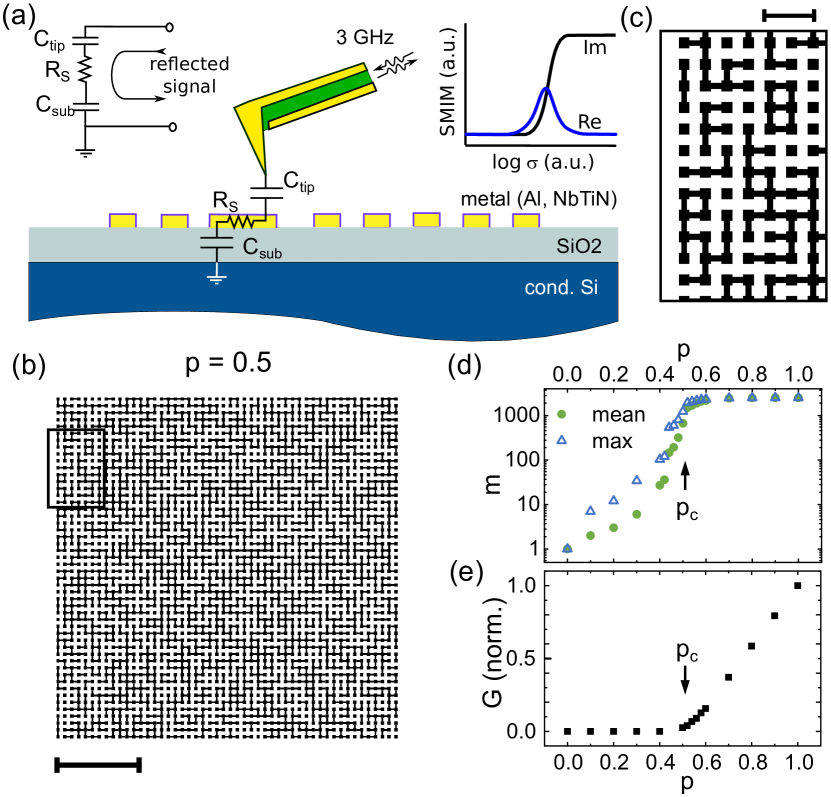
The sMIM used for our experiments is based on an Asylum Cypher Atomic Force Microscope with a PrimeNano Scanwave extension. sMIM uses a shielded cantilever as depicted in Fig. 1(a) to guide a microwave tone to the metallic tip were the signal is reflected back into the cantilever transmission line and fed into a microwave readout circuit Lai et al. (2010, 2008). When the tip (typical apex diameter nm) is far away from the sample, an impedance matching circuit and a common mode cancellation loop suppress signal reflection. As the tip is landed and scanned over a sample, the local material properties in the vicinity of the probe modify the generally complex numbered tip impedance (Fig. 1(a)), giving rise to changes in the real and imaginary component of the reflected microwave signal. The disordered conductor model systems are patterned on a 100 nm thick dielectric SiO2 layer (with relative permittivity ) that covers a conductive Si substrate. The impedance is therefore described in a lumped element circuit in which the substrate acts as a ground plane. The circuit consists of a series network of two capacitors and , representing the coupling between the tip and the sample, and the sample and the substrate, respectively. A resistor takes into account resistive losses inside the network. Hence,
| (1) |
with being the applied frequency (3 GHz). The real and imaginary component of the reflected signal are demodulated in the microwave readout circuit into two dc-signals, which correspond to the resistive (sMIM-Re) and the capacitive (sMIM-Im) component of the tip-sample admittance . The sMIM signal allows for an analysis of material properties because , and are affected on a microscopic level by the electrical conductivity of the conductive patch underneath the tip. Therefore, the signals of sMIM-Im and sMIM-Re are coupled. When changes homogeneously, one obtains characteristic curves for sMIM-Im and sMIM-Re as sketched in the right inset in Fig. 1(a). sMIM-Im exhibits a transition from low to high signal as increases, while sMIM-Re approaches 0 at both extrema and exhibits a peak in between.
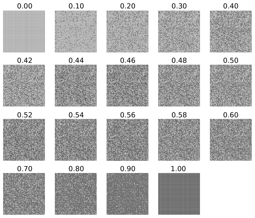
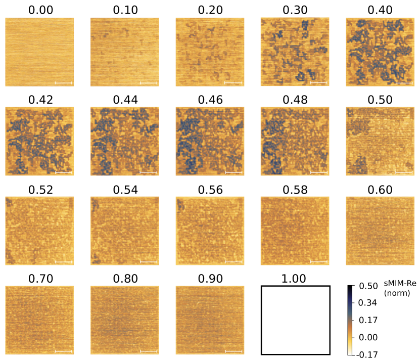
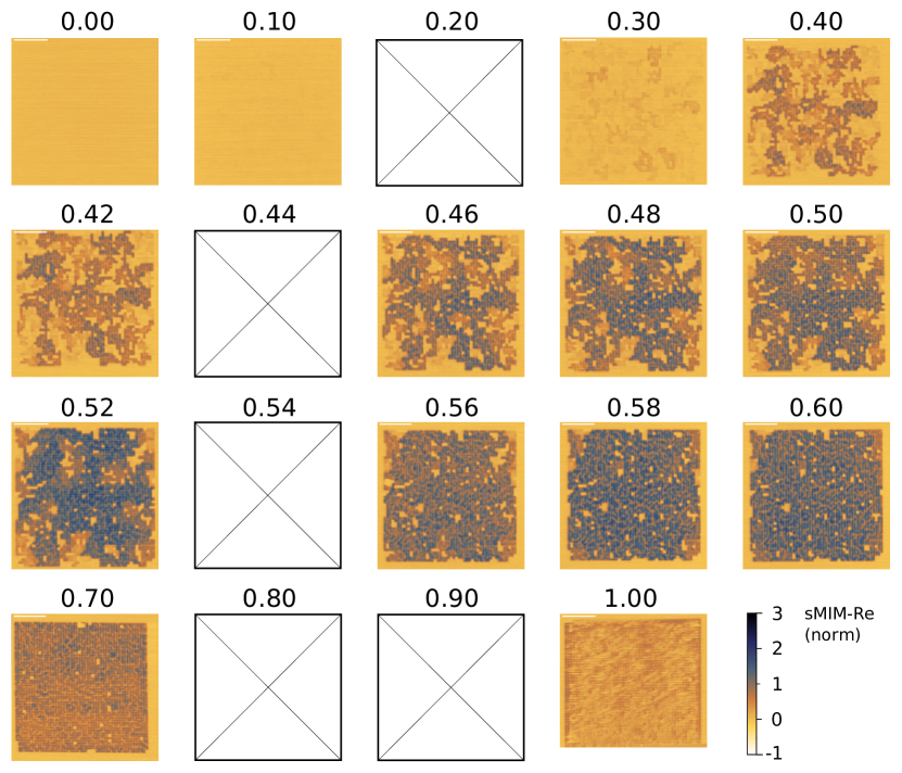
We are interested in the sMIM response for an inhomogeneous sample. Therefore, we have designed a conductor model system consisting of a set of nano-structured metallic two-dimensional bond-percolated networks. We aim to probe the impedance with spatial resolution higher than the scale of disorder and to study spatial variations across the sample as a result of the disordered electrodynamic landscape. Therefore, we design each network to consist of a square grid of nominally nm nm sized, metallic squares which we will refer to as sites. In comparison, the apex diameter of the sMIM tip is of the order of 100 nm. Hence, the sMIM signal can be assigned to the particular site underneath the tip (see SI). Each site can be connected with its 4 nearest neighbours by nm nm metallic bonds. Disorder is introduced by randomly placing only a fraction of bonds in the network. In this fashion, the IMT is modeled by a series of patterns for which the number of bonds increases. Each pattern is then characterized by the total fraction of bonds . The fully insulating state corresponds to an entirely disconnected network with no bonds, . For the fully metallic state . When , clusters of connected sites form, giving rise to a highly disordered pattern as displayed for the case in Fig.1(b) and in the closeup in Fig. 1(c). Each cluster can be characterized by its mass , given by the number of connected sites in that cluster. For small the clusters consist of only a few sites, hence the mean as well as the largest cluster for a given are small [cf. Fig. 1(e)]. As is increased the clusters grow and eventually merge with their neighbors. The IMT coincides with the emergence of the so-called spanning cluster at a critical percolation number . Here, is sufficiently large to establish a continuous conductive path across the whole network, rendering the previously insulating system a conductor at the global scale. This is directly reflected in the conductance , as calculated for each Van Mieghem et al. (2017) between the left and the right edge (see SI for details), which becomes non-zero at , as expected from percolation theory for a 2D square network Stauffer (1979). (The complete set of patterns is shown in the SI.)
We have fabricated the set of patterns from two different materials with different resistivity. It allows us to study the local impedance for a wider range of parameters. As a low resistivity material we choose a 25 nm aluminum (Al) thin film with a sheet resistance , patterned with standard lift-off techniques. As a high resistivity material we use sputtered, 10 nm thick NbTiN Thoen et al. (2016), with .
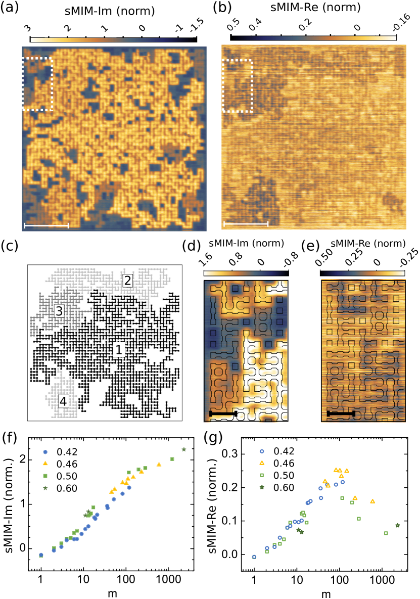
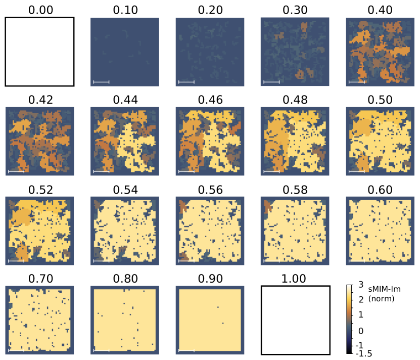
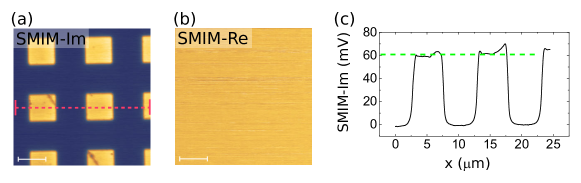
Figure 2 shows typical sMIM images obtained for the network made out of Al with . The data have been normalized with respect to a reference sample (see SI) and they are nulled with respect to the SiO2 dielectric layer. Figure 2(a) shows the imaginary component sMIM-Im, corresponding to capacitive contributions to the impedance. In Fig. 2(b) we show the real part, sMIM-Re, representing the ohmic contributions. Both images reveal a structure that is different from the underlying network depicted in Fig. 1(a). Fig. 2 shows that sMIM-Im, i.e. the capacitance, is large (bright) over large areas, while only smaller patches show a small response (dark). sMIM-Re indicates that ohmic resistance contributes to the impedance only in a few, smaller regions.
Since the pattern was fabricated from a single Al film the observed spatial variations can not be explained with changes in the local conductivity of the Al. We attribute the difference to disorder and thus to the formation of clusters in a network with non-trivial topology.
Figure 2 (c) depicts the network underlying the sMIM data (cf. Fig.1(a)), however, we have removed all sites and bonds from this pattern, except the clusters with the largest cluster mass , labeled 1 to 4. The resulting shape emerging from these clusters strongly resembles the image in Fig. 2(a). This suggests a correlation between the capacitive impedance (sMIM-Im) and the cluster mass . We further observe that areas with a strong sMIM-Re signal coincide with clusters 2, 3 and 4. The connection between cluster mass and impedance appears to hold also for smaller . It can be inferred from the close-up view of sMIM-Im and sMIM-Re in Fig. 2(d) and (e), where we have added the underlying network pattern from Fig. 1(c) as a guide to the eye. Within a cluster the sMIM signals appear to be uniform. We can therefore calculate the mean signal obtained for each cluster and assign the result to the corresponding . This is shown in Figs. 2(f) and (g) for an arbitrary set of clusters, obtained from various Al patterns of different . Figure 2(f) reveals a monotonous increase with for sMIM-Im. The maximum slope occurs approximately around . In contrast, sMIM-Re in Fig. 2(g) exhibits a peak here, while it decreases towards 0 for smaller and approaches a small, but non-zero value towards .
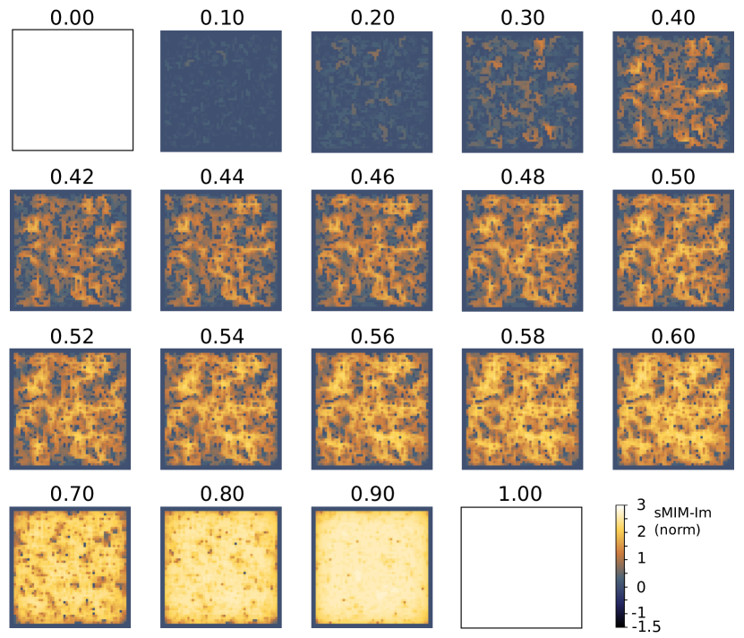
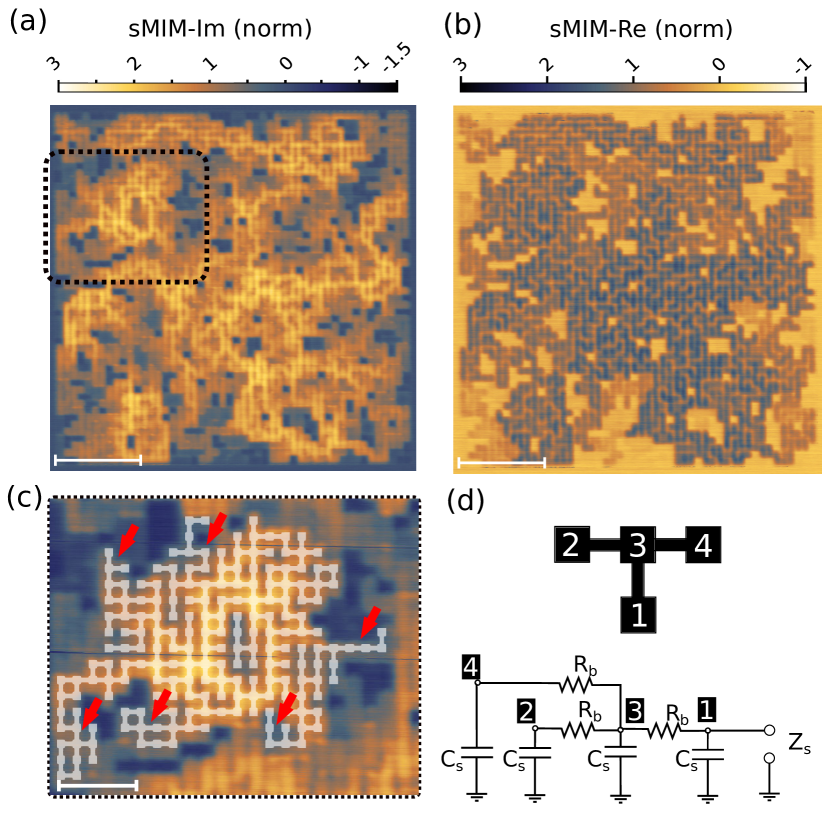
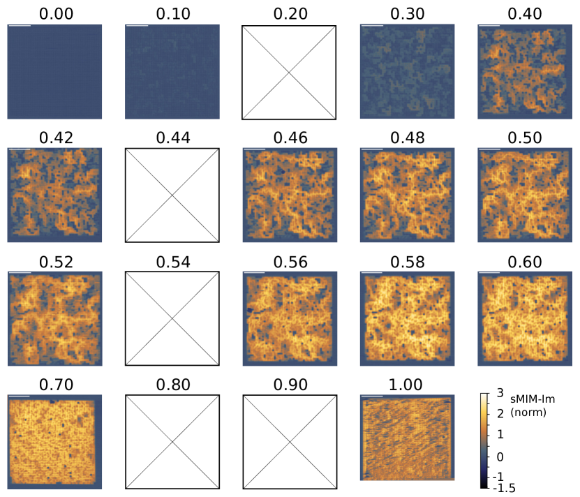
When the exact same network pattern is made from a less conductive material, the corresponding sMIM images change drastically. This is shown in Fig. 3 where the network has been realized from NbTiN. sMIM-Im (Fig. 3(a)) reveals a highly non-uniform distribution of the imaginary impedance that does not bear a clear resemblance with the clusters in Fig. 2(c). Instead, a backbone-type structure becomes visible. sMIM-Re (Fig. 3(b)), in contrast, does not show a backbone structure. Here, the cluster delimitation can be inferred more clearly. However, signal variations within the clusters are significant, which renders an analysis as done for Al in Fig. 2 with sMIM as a function of cluster mass , not applicable. In Fig. 3(c) we therefore directly compare sMIM-Im with the underlying network topology for the region of cluster 3 (cf. Fig. 2 c). We observe that the capacitance (sMIM-Im) is small at the outside branches and polyps of the cluster. It becomes large towards the inside, in particular in a well connected, ring-shaped region, circling the cluster’s center.
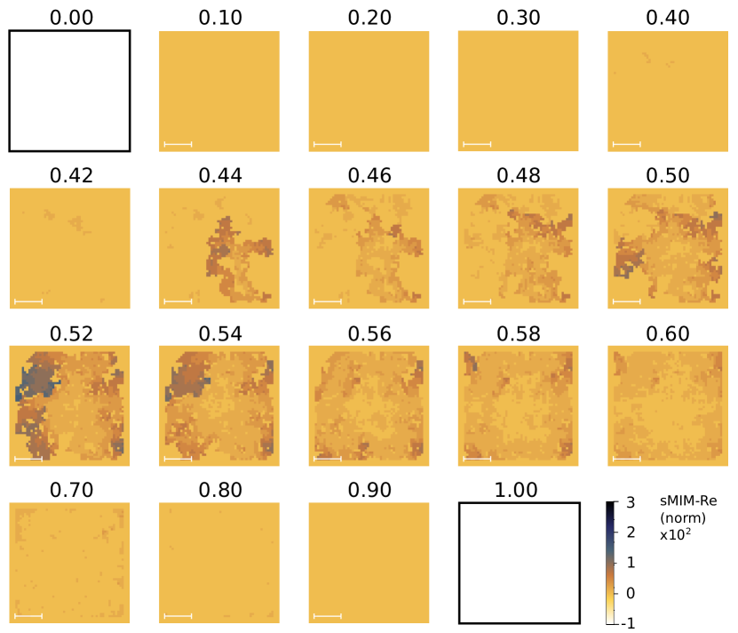
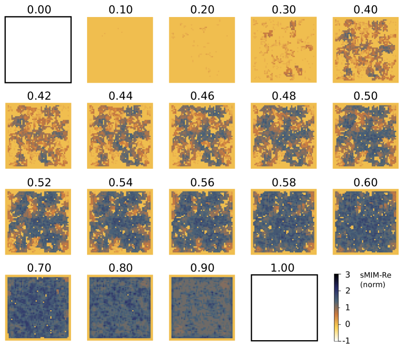
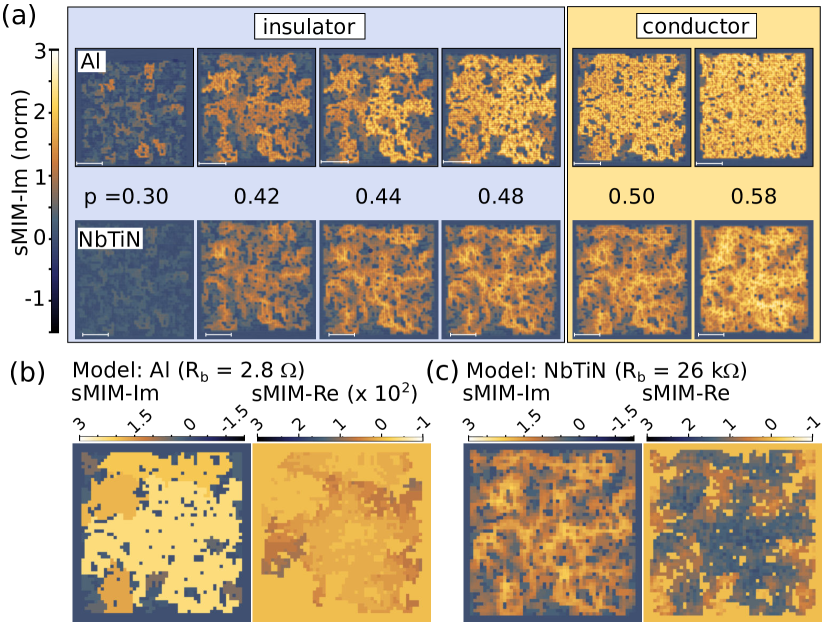
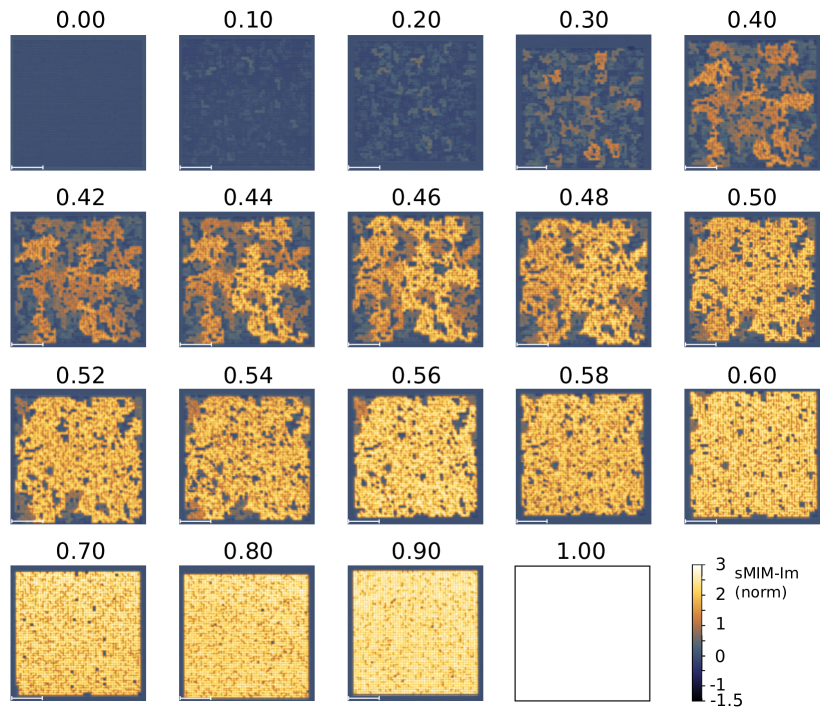
sMIM-Im images of the IMT around are displayed in Fig. 4(a), for Al (top row) and NbTiN (bottom row), highlighting the evolution of the local impedance as structural correlations and network topology evolve.
We can understand the observations in the local impedance within the lumped element picture introduced in Fig. 1(a), taking into account the electrodynamic environment of the scanning probe experiment and the detailed disordered network pattern. We replace the resistor and the capacitor in Eq. 1 by an impedance network that reflects the network topology and the capacitive coupling at each site to the substrate ground plane. Figure 3(d) displays such a network for a small cluster with , with the probe tip positioned at site 1. Each bond connection is represented by a resistor . Each site is taken into account by a capacitor to the substrate.
When is small compared to the impedance of a single site to ground , the microwave currents injected at the probe tip can spread easily across the whole cluster. This applies for Al, where , while M (with fF, see SI). As a result, all site capacitors of a cluster contribute approximately equally to the total capacitance , such that . This explains the absence of variations within a cluster as well as the observed scaling of the capacitive impedance, sMIM-Im, with . However, when becomes sufficiently large, as is the case for NbTiN (), current spreading is impeded. Capacitive contributions to the total impedance, therefore, get suppressed when the sites are connected only through a high resistance current path, for instance via several bonds in series. This is the case at the polyps and dead ends in cluster 3 in Fig.3(c) (arrows). Here the impedance is large due to a small total capacitance . In contrast, in regions where the local connectivity is high, for instance towards the center ring of cluster 3, current injected at the tip can spread over a large number of sites through many parallel current paths. This leads to a smaller impedance due to a large capacitance, and thus to a high sMIM-Im signal. In this picture, the impedance at a particular site reflects the local connectivity of the network, giving rise to the observed backbone type structure.
The RC-network picture indicates how the capacitance to the substrate ground plane may serve as a tuning knob for the range of contrast in a sMIM experiment. Modifying thickness and permittivity of the dielectric will shift the quantitatively sensitive sMIM response to smaller or larger patches of film, i.e. to different scales of disorder.
Based on the RC-network approach, we use a network current spreading model and the pseudo-inverse Laplacian of the underlying network graph Van Mieghem et al. (2017) to compute the impedance at each site and, using Eq.1, to compare it with the experimental data (see SI). The results are shown in Fig. 4 (a) and (b) for Al and NbTiN, respectively. The computed sMIM-Im images reproduce the experimental data (cf. Fig. 2(a) and Fig. 3(a))) very well. The computed sMIM-Re signal (cf. Fig. 2(b) and Fig.3(b)), however, deviates more from the experiments. Interestingly, while for NbTiN deviations are small and mainly occur in samples with larger (see SI), deviations are particularly strong for Al, where the sMIM-Re signal magnitude, compared to the corresponding sMIM-Im, is orders of magnitude smaller than in the experiments. The differences between the model prediction and the data on Al therefore suggest that the simple RC network model used here is incomplete.
The present experiments highlight the electrodynamic environment of the tip provided by the inhomogeneous sample. It is reminiscent of the importance of the electrodynamic environment in scanning tunneling experiments, such as in a Josephson current based tunneling experiment (for example Ast et al. Ast et al. (2016)). Here, the metallic tip of the scanning probe acts as a resonant antenna interacting with the Josephson oscillations. Our experiments indicate that for electrically inhomogeneous materials, such as a structured film of Al or disordered superconductors such as NbTiN, TiN or InO Sacépé et al. (2008); Dubouchet et al. (2019) the sample under study also contributes to the effective electrodynamic environment.
Finally, we note that it may be an interesting route in the future to explore techniques to invert the procedure described here, i.e. to construct the underlying disordered network in an unknown material from a sMIM image.
In conclusion, we have studied experimentally the role of disorder for the local impedance in a percolating conductor model system using microwave impedance microscopy. We find that structural properties such as cluster size, network topology and local connectivity can significantly influence the local electrodynamic environment, depending on the material resistivity and the degree of disorder in the system.
Acknowledgements.
We like to thank David J. Thoen for help with the NbTiN sample fabrication. We acknowledge funding through the European Research Council Advanced Grant No. 339306 (METIQUM).References
- Basov et al. (2011) D. N. Basov, R. D. Averitt, D. Van der Marel, M. Dressel, and K. Haule, Reviews of Modern Physics 83, 471 (2011).
- Kirkpatrick (1973) S. Kirkpatrick, Reviews of modern physics 45, 574 (1973).
- Van Mieghem (1992) P. Van Mieghem, Reviews of modern physics 64, 755 (1992).
- Gantmakher and Dolgopolov (2010) V. F. Gantmakher and V. T. Dolgopolov, Physics-Uspekhi 53, 1 (2010).
- Qazilbash et al. (2007) M. M. Qazilbash, M. Brehm, B.-G. Chae, P.-C. Ho, G. O. Andreev, B.-J. Kim, S. J. Yun, A. Balatsky, M. Maple, F. Keilmann, et al., Science 318, 1750 (2007).
- Keimer and Moore (2017) B. Keimer and J. Moore, Nature Physics 13, 1045 (2017).
- Soumyanarayanan et al. (2016) A. Soumyanarayanan, N. Reyren, A. Fert, and C. Panagopoulos, Nature 539, 509 (2016).
- Rosner and Van Der Weide (2002) B. T. Rosner and D. W. Van Der Weide, Review of Scientific Instruments 73, 2505 (2002).
- Huber et al. (2008) A. J. Huber, F. Keilmann, J. Wittborn, J. Aizpurua, and R. Hillenbrand, Nano letters 8, 3766 (2008).
- Lai et al. (2010) K. Lai, M. Nakamura, W. Kundhikanjana, M. Kawasaki, Y. Tokura, M. A. Kelly, and Z.-X. Shen, Science 329, 190 (2010).
- Ma et al. (2015a) E. Y. Ma, M. R. Calvo, J. Wang, B. Lian, M. Mühlbauer, C. Brüne, Y.-T. Cui, K. Lai, W. Kundhikanjana, Y. Yang, et al., Nature communications 6, 7252 (2015a).
- Gramse et al. (2017) G. Gramse, A. Kölker, T. Lim, T. J. Stock, H. Solanki, S. R. Schofield, E. Brinciotti, G. Aeppli, F. Kienberger, and N. J. Curson, Science advances 3, e1602586 (2017).
- Atkin et al. (2012) J. M. Atkin, S. Berweger, A. C. Jones, and M. B. Raschke, Advances in Physics 61, 745 (2012).
- Anlage et al. (2007) S. M. Anlage, V. V. Talanov, and A. R. Schwartz, in Scanning probe microscopy (Springer, 2007) pp. 215–253.
- Ma et al. (2015b) E. Y. Ma, Y.-T. Cui, K. Ueda, S. Tang, K. Chen, N. Tamura, P. M. Wu, J. Fujioka, Y. Tokura, and Z.-X. Shen, Science 350, 538 (2015b).
- de Visser et al. (2016) P. J. de Visser, R. Chua, J. O. Island, M. Finkel, A. J. Katan, H. Thierschmann, H. S. van der Zant, and T. M. Klapwijk, 2D Materials 3, 021002 (2016).
- Lai et al. (2008) K. Lai, W. Kundhikanjana, M. Kelly, and Z. Shen, Review of scientific instruments 79, 063703 (2008).
- Huber et al. (2012) H. Huber, I. Humer, M. Hochleitner, M. Fenner, M. Moertelmaier, C. Rankl, A. Imtiaz, T. Wallis, H. Tanbakuchi, P. Hinterdorfer, et al., Journal of Applied Physics 111, 014301 (2012).
- Gramse et al. (2014) G. Gramse, M. Kasper, L. Fumagalli, G. Gomila, P. Hinterdorfer, and F. Kienberger, Nanotechnology 25, 145703 (2014).
- Buchter et al. (2018) A. Buchter, J. Hoffmann, A. Delvallée, E. Brinciotti, D. Hapiuk, C. Licitra, K. Louarn, A. Arnoult, G. Almuneau, F. Piquemal, et al., Review of Scientific Instruments 89, 023704 (2018).
- Van Mieghem et al. (2017) P. Van Mieghem, K. Devriendt, and H. Cetinay, Physical Review E 96, 032311 (2017).
- Stauffer (1979) D. Stauffer, Physics reports 54, 1 (1979).
- Thoen et al. (2016) D. J. Thoen, B. G. C. Bos, E. Haalebos, T. Klapwijk, J. Baselmans, and A. Endo, IEEE Transactions on Applied Superconductivity 27, 1 (2016).
- Ast et al. (2016) C. R. Ast, B. Jäck, J. Senkpiel, M. Eltschka, M. Etzkorn, J. Ankerhold, and K. Kern, Nature communications 7, 13009 (2016).
- Sacépé et al. (2008) B. Sacépé, C. Chapelier, T. Baturina, V. Vinokur, M. Baklanov, and M. Sanquer, Physical review letters 101, 157006 (2008).
- Dubouchet et al. (2019) T. Dubouchet, B. Sacépé, J. Seidemann, D. Shahar, M. Sanquer, and C. Chapelier, Nature Physics 15, 233 (2019).
- Nečas and Klapetek (2012) D. Nečas and P. Klapetek, Open Physics 10, 181 (2012).
- Pozar (2009) D. M. Pozar, Microwave engineering (John Wiley & Sons, 2009).
- Jouve et al. (1996) G. Jouve, C. Severac, and S. Cantacuzene, Thin Solid Films 287, 146 (1996).
I Supplementary Information
I.1 sMIM reference sample
In order to be able to directly compare sMIM data obtained from different structures, we use as a reference sample consisting of m m Al squares on , as provided by the sMIM manufacturer PrimeNano Inc (Fig.S1). While collecting the data from the NbTiN and Al networks, we frequently scanned the reference sample. This allows us to normalize the sMIM data for each network shown in the main text, with respect to the mean contrast in the sMIM-Im channel obtained from the reference sample. In this manner the sMIM data for different structures become comparable and signal changes due to tip wear-off of electronic drift get removed.
I.2 Topography characterization of networks
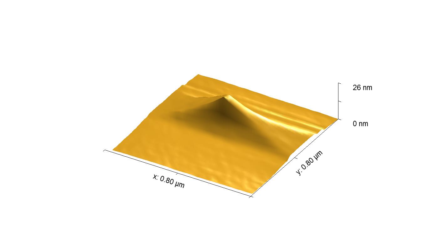
Figure S2 (a) and (b) depict topography line scans of two disconnected sites fabricated out of Aluminum and NbTiN, respectively. Note that these scans were taken with a different, sharper tip than the one used for the sMIM measurements. While the size of the NbTiN sites ( nm) is close to the nominal value (200 nm), the Al site is larger ( nm). This is a result of the different fabrication techniques, which consisted of a lift-off process for Al, and a dry-etch step for the NbTiN sample.

I.3 Contributions on the sMIM signal from neighboring sites

I.4 Tip shape estimate
I.5 Disordered conductor model systems
I.6 Calculation of model parameters , and
The capacitance between a single site and the substrate ground plane is calculated using a textbook closed-form expression for a microstrip line Pozar (2009) (corresponding to metallic plate above an infinite ground plane), with the goal to use a simple approximation that also takes into account stray fields.
| (2) |
with site dimensions nm (estimated from the topography images), dielectric thickness nm, the dielectric constant and the vacuum speed of light . This yields fF.
The tip-site capacitance is calculated in a similar fashion. From the topography images obtained along with the sMIM data, we infer that the sMIM tip is strongly worn down (cf. blind tip estimate in Fig. S4). We empirically find good agreement for fF, corresponding, in a parallel plate capacitor model, to a tip size of 200 nm interacting capacitively with the sample, and 1 nm thin layer of natural covering the Al structures ().
Using this value to model the experiments on NbTiN also yields good agreement. This is a surprising since obviously these structures are not expected to be exhibit an layer. However, while little is known about the oxidation of NbTiN structures under ambient conditions, some studies suggest that a dielectric film is formed Jouve et al. (1996). In our case, even though dielectric constant and thickness of such a film are likely to be different compared to the Al samples, apparently the resulting is of similar order.
The resistance of each bond, is calculated using the measured sheet resistance ( , k) and the geometry of the bond connection nm and nm. Including the resistance of half a site on each side of the bond connection adds to the bond resistance, . This yields and , as used in the main text.
I.7 Impedance network model
In order to calculate the electrical properties of our disordered conductor model systems we follow an approach described by Van Mieghem et al. in Ref. Van Mieghem et al. (2017). We convert each of the percolated conductor patterns shown in fig. S5 into a matrix and construct the corresponding weighted adjacency matrix , yielding an matrix ( being the total number of sites) which only has non-zero entries if the sites and are directly connected through a single bond in . The capacitive connection to the substrate ground plane in the experiments is taken into account by adding a ground node to that is directly connected to every other site via the complex impedance . This yields the modified adjacency matrix from which we can construct the Laplacian
| (3) |
The complex effective impedance between the two nodes and is then given by Van Mieghem et al. (2017)
| (4) |
where is the pseudo-inverse of the weighted Laplacian .
The local impedance of the network at each site , as relevant in our experiment, is then obtained by calculating the impedance between site and the ground node, .
In addition to , signal reflection at the cantilever tip is also determined by the capacitive tip-site coupling, . Hence,
| (5) |
The dissipative and capacitive component of the measured sMIM signal as plotted in Fig. 4 (a) and (b) in the main text, sMIM-Im and sMIM-Re, are then obtained by taking the real and imaginary components of the total admittance for each site in the network.
The macroscopic conductance between the left and the right edge of each pattern as plotted in Fig.1(d) in the main text, is obtained by summing up the conductance between each site on the left edge and all the sites of the right edge. is then given by the real component of the result. Since corresponds to a dc conductance, we ensure that contributions from ac currents through the ground node are suppressed in this calculation by letting .
I.8 Additional sMIM data
I.9 Results of the network model calculation