Subnanometer imaging and controlled dynamical patterning of thermocapillary driven deformation of thin liquid films
Abstract
Exploring and controlling the physical factors that determine the topography of thin liquid dielectric films are of interest in manifold fields of research in physics, applied mathematics, and engineering and have been a key aspect of many technological advancements. Visualization of thin liquid dielectric film topography and local thickness measurements are essential tools for characterizing and interpreting the underlying processes. However, achieving high sensitivity with respect to subnanometric changes in thickness via standard optical methods is challenging. We propose a combined imaging and optical patterning projection platform that is capable of optically inducing dynamical flows in thin liquid dielectric films and plasmonically resolving the resulting changes in topography and thickness. In particular, we employ the thermocapillary effect in fluids as a novel heat-based method to tune plasmonic resonances and visualize dynamical processes in thin liquid dielectric films. The presented results indicate that light-induced thermocapillary flows can form and translate droplets and create indentation patterns on demand in thin liquid dielectric films of subwavelength thickness and that plasmonic microscopy can image these fluid dynamical processes with a subnanometer sensitivity along the vertical direction.
I Introduction
Determining the topography of TLD films is of fundamental importance for the basic studies of interfacial science such as the study of wettability and spreading craster2009dynamics , the study of the response to external stimuli in both physical oron1997long and biological systems grotberg2001respiratory , and studies related to numerous industrial applications such as coatings, insulating layers and surface modifiers (yerushalmi1994suppression, ; senaratne2005self, ). While one of the commonly used methods to determine the thickness of TLD films is white-light interferometry, the sensitivity of this method to local small thickness variations is low, especially when the film thickness is less than the optical wavelength due to the low reflection from the film’s surface. One attractive possibility to enhance this sensitivity is to utilize strong coupling between collective oscillations of electrons in the metal (surface plasmons) to the resulting radiated electromagnetic field (the polariton), which supports surface plasmon polaritons (SPPs) - electromagnetic waves that propagate along the metal-dielectric interface and strongly decay in the direction perpendicular to it raether2013surface . This localization property makes SPPs very sensitive to the dielectric properties of materials in close proximity to the metal surface, which, over the last few decades, has led to a wide spectrum of sensing and imaging techniques, such as surface plasmon spectroscopy and surface-plasmon resonance microscopy (SPRM) rothenhausler1988surface . In particular, SPRM is a well-established method for label-free imaging of low contrast features such as the roughness of thin solid dielectric films sadowski1995characterization , imaging of small biological objects such as bacteria, viruses, and biofilms, and the detection of analytes as a result of surface reactions. The latter typically results in a few nanometer-thick monolayer array of molecules bound to metal surfaces, which modifies the SPP momentum (e.g., by changing the refractive index), and numerous applications such as the biosensing of surface reaction events lofas1991bioanalysis ; homola2006surface and cell adhesion sites watanabe2012scanning , have been found. Unlike alternative methods suited to characterizing nanometric and subnanometric topographies, such as atomic force microscopy (AFM), which are scanning imaging techniques, SPRM is an optical technique that can flexibly measure topographies in both wide-field imaging and scanning confocal modes. Moreover, SPRM is a noncontact method that avoids the sample-specific mechanical interactions involved in AFM imaging. In particular, for fluid topometry (i.e., topography measurement), noncontact optical imaging avoids sensitive perturbations to the TLD dynamics that would otherwise be inevitable with contact mechanical probing.
In this work, we demonstrate for the first time a combined imaging and optical patterning projection platform, that is capable of optically inducing dynamical processes in TLD films and then measure subnanometric topographic and thickness changes. Specifically, the optically projected pattern induces thermal gradients which in turn trigger thermocapillary (TC) flows, while SPRM imaging leverages the near-field profile of surface plasmon resonances to resolve and characterize the sub-nanometric topographies of flow-induced interface perturbations. Analogous to traditional pump-probe systems, our system uses a heating pump beam to invoke TC flows and is capable of probing the accompanying deformation of the TLD film.
In our work we introduce local changes in TLD film thickness by taking advantage of the characteristic optical absorption in metals (i.e., unrelated to the SPP-driven heating), which stimulates the TC effect levich1962physicochemical . The latter is a special case of the Marangoni effect, which is manifested by TC flows and the deformation of a TLD film due to the spatially non-uniform temperature distribution of the liquid-gas interface and subsequent spatial variations of the surface tension. Notably, in previous works, heat-induced tuning of the SPP coupling condition was mostly invoked by thermo-optic and phase transition effects (see vivekchand2012liquid and references therein); in our work, heat-generated SPP tuning is experimentally triggered for the first time by a fundamentally different mechanism that stems from geometrical changes of the TLD film topography, as was recently theoretically demonstrated rubin2018nonlocal .
Previous studies that applied SPRM imaging to thin dielectric films, such as huang2007surface , focused on solid and static films and did not employ the SPRM method to study fluid dynamical processes. Furthermore, while TC-induced patterning has received significant attention in the past, mostly in the context of thin polymer film molding, where TC flows are triggered only in regions where the polymer film is above the glass phase transition temperature singer2016focused (and also singer2017thermocapillary and references therein), we here leverage the ability to induce optically desired heating patterns to demonstrate the formation of light-induced droplets of different size directly from TLD film and their translation along the substrate (see also yoo2015directed and han2017controllable , which report the formation of droplets from amorphous silicon and gold by employing phase plates). To the best of our knowledge, previous studies in micro- and nanofluidics reported controlled droplet formation in microchannels by employing directional flows of several liquid phases (see zhu2017passive for a recent review and references therein) and by utilizing a light-driven TC effect baroud2007thermocapillary ; however, these studies did not employ optical patterns to take advantage of the TC effect for the formation and translation of microdroplets directly from stationary TLD films without microchannels.
We experimentally employ traditional SPRM to image the dynamical depth changes and 3D nanoscale topography of the TLD film in a subwavelength thickness regime, which is challenging for purely interferometric methods. A numerical model is constructed that relates TLD thickness to the measured SPP coupling angle, allowing for the experimental determination of the TLD topography and local thickness from a series of SPRM frames. While in our work we experimentally determined the topography of TLD films with a mean thickness comparable to or smaller than the penetration depth of an SPP mode in the direction normal to the metal surface, we theoretically note that in principle, it is possible to achieve similar sensitivity for subnanometer thickness changes of significantly thicker TLD films by leveraging waveguide (WG) modes, which admit the highest optical intensity within the film.
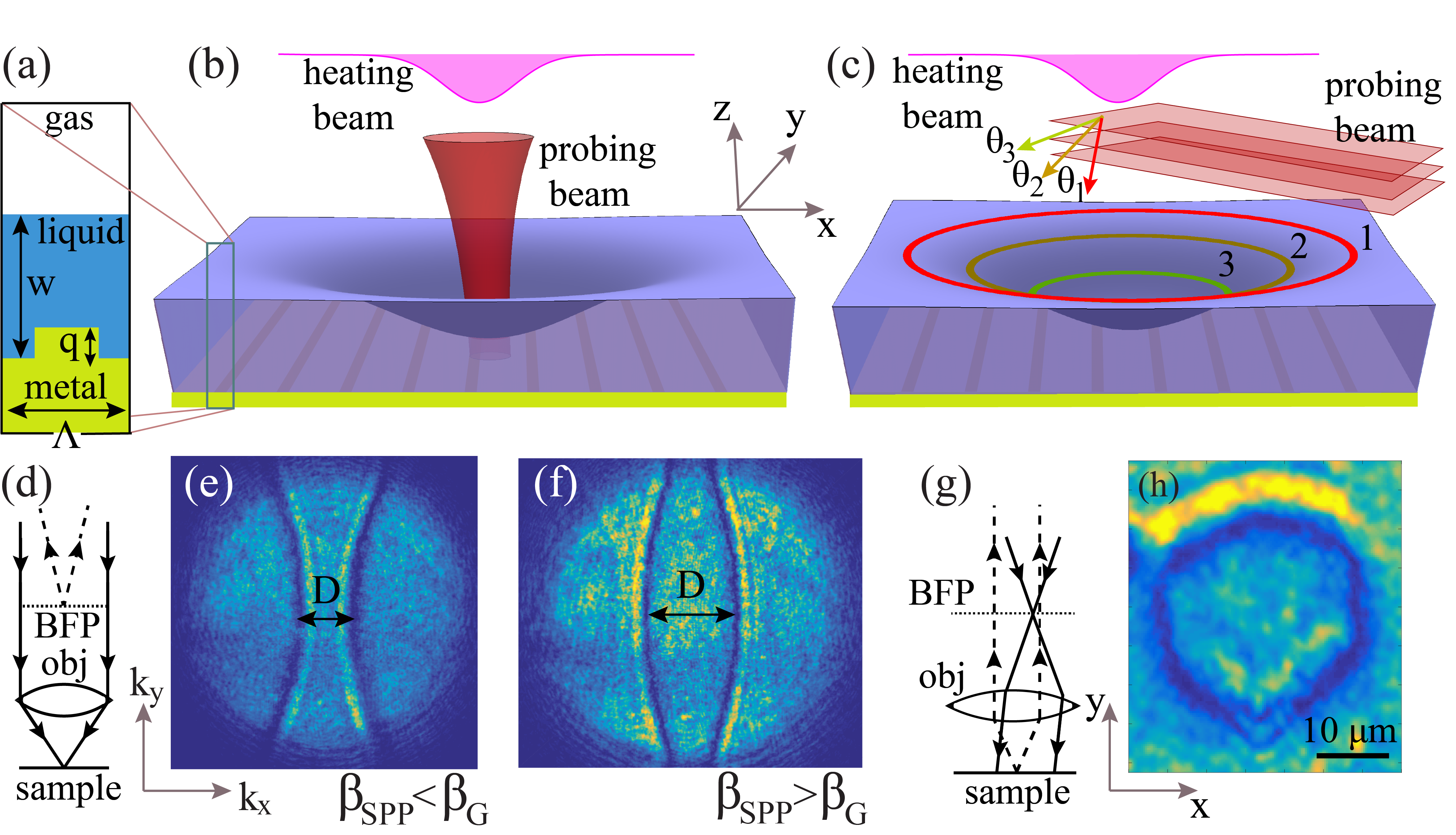
To illustrate the optical interaction with the TLD film for both manipulation and imaging, Fig. 1(a) presents key elements of our system under study: a metal grating of period and wave vector and an adjacent layer of the TLD film of thickness , as measured from the bottom part of the grating grooves. Our imaging methods rely on capturing the angular and spatial content of the beam reflected from the sample, referred to below as space and real-space imaging, which correspond to the monochromatic coupling illumination configurations described in Fig. 1(b,d) and Fig. 1(c,g), respectively. space imaging utilizes a probing focused Gaussian beam, produced by a collimated beam filling the objective back focal plane (BFP), which corresponds to a focused beam on the sample (Fig. 1(b,d)). Real-space imaging on the other hand, utilizes the dual configuration with a plane wave made incident at a specified angle on the sample (Fig. 1(c)), which corresponds to a focused beam at the BFP (Fig.1(g)). Both methods take advantage of the fact that the magnitude of the corresponding SPP momentum, , is a strictly increasing function of the TLD film thickness which allows the construction of a one-to-one correspondence between the film thickness and the SPP resonant coupling angle.
Fig. 1(e,f) presents representative space imaging results of the BFP with inward and outward facing dark arcs separated by a distance along the central line, which correspond to different SPP coupling regimes depending on the sign of the difference . Importantly, the distance , which in our work can depend on time, together with the inward or outward pointing configuration of the dark arcs, uniquely sets the SPP coupling angle and the corresponding TLD film thickness at the focal point (see kvasnivcka2014convenient for BFP imaging due to reflectance from a metal grating covered with a solid dielectric film). The emergent patterns are related to the Kikuchi patterns or Kossel lines that have been observed in atomic structures through electron microscopy and Brillouin zone spectroscopy of photonic crystals bartal2005brillouin . In the real-space imaging setup (Fig. 1(c,f)), the regions of low reflected light are indicative of spatial regions where the resonant coupling condition of the incident plane wave into the SPP mode holds. Fig. 1(h) presents a representative image of a wide field of view of a few tens of microns showing a dark contour indicative of fluid thickness that supports the SPP coupling condition at the illumination angle. By sweeping the incidence angle with the same source wavelength, one can then obtain a set of resonant curves that correspond to a set of level thickness contours where the incident plane wave couples to the SPP, which is schematically shown in Fig. 1(c).
II Governing equations
Thin liquid film deformation due to optically induced thermocapillary effect
The topography of a TLD film is determined by the internal stress balance between capillary and viscous forces, as well as by external stimuli. Assuming a Newtonian fluid of viscosity (which holds for the silicone oil employed in our work), considering linear dependence of the surface tension, , on the temperature difference levich1962physicochemical given by
| (1) |
and applying the lubrication approximation for the corresponding linearized Navier-Stokes equation oron1997long yields the following equation for the TLD film deformation under spatiotemporal-dependent optical intensity ,
| (2) |
(see rubin2018nonlocal and Supplementary Material). Here, is the so-called Marangoni constant; is the dimensionless Marangoni number, which represents the ratio between the surface tension stresses due to the TC effect and dissipative forces due to fluid viscosity and thermal diffusivity in a film of height ; is the dimensionless intensity of the heat source; is the typical length scale along the in-plane direction; is the characteristic optical power scale; is the heat diffusion coefficient; , , , and are the mass density, specific heat, heat conductance, and optical absorption coefficient of the metal substrate, respectively; is the characteristic heat diffusion time scale in the metal; is the typical thin film deformation time scale; and . Importantly, the negative (positive) sign of the source term in Eq.(3) indicates that local regions of higher (lower) temperature lead to a local decrease (increase) in TLD film thickness.
Coupling of SPP into grating covered with dielectric
Grating coupling is a common method to evanescently excite SPPs from free-space modes (see homola2006surface and references therein). Assuming that a plane wave with a wave vector component parallel to the grating, , is made incident on a metal surface with a grating of period gives rise to a series of diffracted waves with wave vectors given by , where is the grating vector that is perpendicular to the grating grooves (aligned along the direction as described in Fig. 1) and is the diffraction order. The diffracted waves along the interface can couple to an SPP mode provided the following momentum balance equation holds raether2013surface :
| (3) |
where , and is the SPP momentum raether2013surface . Here, is the resonance coupling angle of incoming light, is the magnitude of a free-space wavenumber vector of wavelength , and and denote the dielectric constants of the metal and dielectric, respectively. Inserting the definitions of , and into Eq.(3) yields the following expression for :
| (4) |
where . Treating the TLD film and air bilayer as a single medium with a depth-averaged index, obtained by integrating the index distribution along the direction normal to the metal surface campbell1998quantitative , we learn that the resonant coupling angle is a strictly decreasing function of the TLD film thickness. In particular, as the TLD film thickness increases in the range , the resonant coupling angle tends to a normal incidence condition at critical thickness . For higher thickness values, i.e., for , the coupling angle becomes negative, which corresponds to a transition from the counter-propagating to the co-propagating regime of the coupled SPP mode (see Fig.S1 in Supplementary Material). To obtain a quantitative model that predicts the TLD film thickness (without approximations such as the depth averaging mentioned above) based on an experimentally measured resonant coupling angle, we turn to a numerical simulation (using Lumerical FDTD). While in real-space imaging the resonant coupling angle coincides with the predetermined illumination angle, in -space imaging, the resonant coupling angle can be inferred from the distance between the dark arcs, , shown in the representative experimental images of Fig. 1(e,f), via
| (5) |
where and can be functions of time due to thickness changes of the TLD film.
Experimental setup
We employ two different laser sources, the so-called heating- and probing beams described in Fig. 1, which are coupled to the same optical path, and deliver them to the sample. An argon laser (, nm) is used as the heating beam, which heats the metal substrate by optical absorption of the projected pattern and invokes TC flows accompanied by deformation of the TLD film; an NIR laser diode ( nm) is used as the probing beam, which, upon reflection provides an angular and spatial map for resonant SPP coupling.
For a case of large deformations of the TLD film, which are within the reach of standard white-light microscopy, we employed a similar experimental setup, with a nm heating beam. An epi collection microscope was used to deliver both beams and image the fluid response (Olympus). The heating beam was collimated, optionally passed through a beam-shaping or transparency element, and then passed through a X microscope objective (Mitutoyo) and focused to a point with a m width (FWHM). The probing beam was delivered to the microscope objective in one of two configurations: collinear with the pump beam as a plane wave and focused on the sample (real-space imaging) and focused on the objective BFP and delivered to the sample as a plane wave (k-space imaging), both described in Fig. 1(d) and Fig. 1(g), respectively. In the first configuration, the probing-beam was then epi collected, and the BFP was imaged to measure the angular spectrum up to the objective numerical aperture, where the input angles satisfying the SPP momentum conditions appear as absorption lines in the angular spectrum. Changes in the momentum condition owing to the thickness change due to TC and healing flows were visualized as shifts in the resonance angle. In the second configuration, the collimated probing beam was passed through a lens (f = cm) on a lateral translation stage and focused onto the BFP for Köhler illumination. Lateral displacements of the lens shifted the focus across the BFP, thus shifting the plane wave angle of incidence at the grating. The collected light was imaged by the microscope tube lens for direct observation of the grating surface, and regions with TLD film thickness matching the SPP condition at a given angle of incidence could be observed to darken according to resonant absorption. Because of the large thickness range in the fluid layer after the TC flow, sweeping of the illumination angles allowed visualization of the resonant contours of the corresponding level regions with thicknesses supporting the SPR resonance at the given angle. To form the TLD film, silicone oil of refractive index was spun onto the fabricated gold grating (see Supplementary Material for more details).
III Model for TLD film thickness determination
Extracting the TLD film thickness from experimental measurements requires a theoretical model that relates the thickness of the TLD film to the resonant coupling angle of the substrate guided modes. Fig. 2 presents numerical simulation results of an incident plane wave coupling into propagating SPP and WG modes on a metal grating covered with a TLD film by using Lumerical FDTD. The key components of the simulation domain, presented schematically in Fig.1(a), consist of an incoming plane wave of wavelength nm, grating period nm, and grating depth nm. The dielectric constant of gold at nm and the refractive index of silicone are taken as johnson1972optical and , respectively (see Supplementary Material for additional details). Fig. 2(a) presents the resonant coupling angle curves and into an SPP mode and into a higher-order WG mode (which emerges at higher thickness values aust1994surface ), respectively, as a function of the TLD film thickness .
Importantly, both are strictly decreasing functions of and therefore can be used to construct an inverse function where can be deduced based on the values of . The regions of positive and negative values of the function correspond, respectively, to SPP modes that propagate in a counter- and co-propagating direction relative to the in-plane component of the incident plane wave. These two different regimes are separated by an angular band gap centered at the normal incidence angle (see Supplementary Material section), which is reminiscent of the band gap observed near normal incidence conditions on metal gratings without a dielectric layer pang2007observation due to destructive interference of the left- and right-propagating SPP modes. The filled curves in Fig. 2(a) present the corresponding sensitivity for the SPP and the higher-order WG mode, defined as and , respectively. While the SPP mode admits the highest sensitivity value for a film thickness of approximately nm and practically vanishes for thickness values above nm, the first WG mode (which does not emerge at low thicknesses) admits the highest sensitivity at approximately nm. These differences in regions of maximal sensitivity stem from the fact that, while for sufficiently thin films, the incoming plane wave couples to an SPP mode that admits the highest optical intensity on the metal surface (see Fig. 2(c)), for thicker films the incident plane wave couples into a higher-order WG mode with the highest optical intensity at some finite distance from the metal surface within the TLD film, as presented in Fig. 2(d) (see also tobias2007theoretical for optical intensity distribution along the vertical direction in dielectric-loaded SPP waveguides). Interestingly, the sensitivity of the WG modes drops in close proximity to the cutoff thickness values (i.e., film thickness that satisfies the WG cutoff condition kogelnik1974scaling ), seen around nm in the center of the dashed region in Fig. 2(a). As presented in Fig.2(b) one could potentially mitigate these lower-sensitivity regions by employing either a longer wavelength probing beam which can couple to an SPP mode, or alternatively a shorter wavelength probing beam which can couple to a WG mode, without modifying the grating properties.
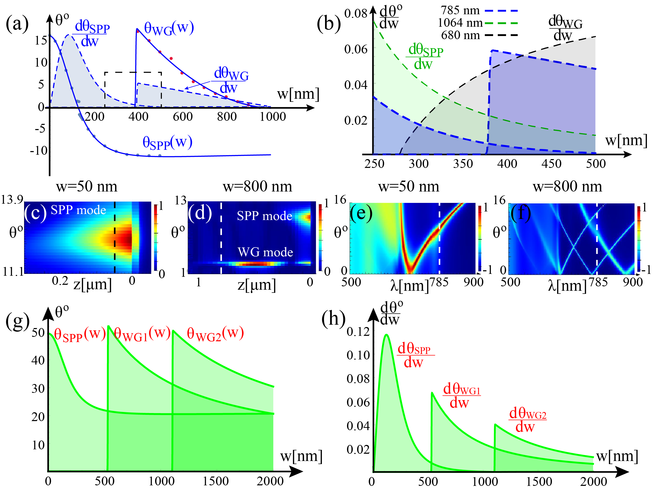
Fig. 2(e) presents the dispersion relation of the basic SPP mode, which is coupled to the metal grating that hosts a nm dielectric. In particular, it shows a single curve, where the right and left branches correspond, respectively, to counter- and co-propagating modes relative to the in-plane component of the incident plane wave. The dashed vertical line at nm, which corresponds to the wavelength of the probing beam, intersects with the right branch, indicating that the given conditions facilitate coupling only to the counter-propagating SPP mode at a resonant coupling angle of . Since the dispersion relation of WG modes propagating in a slab WG (formed, in our case by the TLD film) is set by the constructive interference condition kogelnik1974scaling , it follows that additional higher-order WG modes must emerge at even higher thickness values of the TLD film. Indeed, Fig. 2(f) presents an additional higher mode that emerges in thicker films of thickness nm. The dashed vertical line of the probing beam at nm intersects with a left (co-propagating) branch of the SPP curve at and with the right branch of the first WG mode at .
Fig. 2(g) presents resonant coupling angle as a function of film thickness for the SPP mode as well as for the first and the second WG modes, for the case of a longer wavelength ( nm) probing-beam, whereas Fig.2(h) presents the corresponding sensitivity curves. Similarly to the case of the nm probing-beam described above, thicknesses around the cutoff condition of each one of the WG modes are accompanied by lower sensitivity regions. As expected, employing higher wavelength allows to extend the sensitivity range for higher film thicknesses due to higher penetration depth of the corresponding SPP mode into the dielectric region; for instance a sensitivity of /nm can be achieved by employing nm wavelength at thickness nm or by employing nm wavelength at thicknesses nm or nm. It is instructive to mention that in our work SPP and WG modes admits more than an order of magnitude higher sensitivity than the FP (Fabry-Perot) reflectance commonly used in white light microscopy (see Supplementary Material).
IV Experimental results
IV.1 Dynamical optical manipulation of TLD films
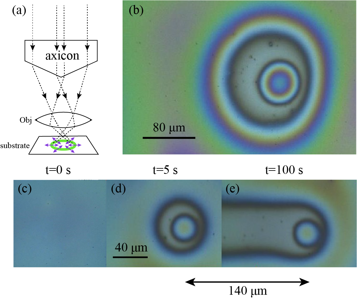
To probe optical control over the shape of the liquid-gas interface, we employed a novel optical patterning system to deliver light illumination through a beam-shaping element. The delivered light pattern induces a thermal gradient on the liquid-gas interface and consequently triggers TC flows, which allow manipulation of its shape. In particular, fixing an axicon beam-shaping element to the Fourier plane of the objective lens transforms the substrate plane focal point into a focused ring-shaped illumination pattern on the substrate (Fig. 3(a)) and leads to TC flows that invoke film thinning in the regions of highest temperature. Fig. 3(b) presents a white-light microscopy image of the generated droplet of approximately m in diameter from a nm thick silicone oil film, spun on a NiCr substrate, due to a mW laser source of wavelength nm and an illumination time of s. Film deformations were measured using a white-light reflection microscope (Leica, 50X) and a X objective. Fig. 3(c-e) present droplet formation from a thinner nm thick silicone oil film and droplet translation along the metal substrate, achieved by translating the microscope stage and keeping all other components of the optical setup stationary. In this case, we utilized a higher magnification objective, X, which resulted in a higher optical power and consequently shorter illumination time of s. The speed of stage translation in our experiments was approximately m/s, which was sufficiently low to ensure that the invoked TC flows in the silicone oil film around the droplet led to a ring-shaped rupture as the optical pattern was progressively translated along the substrate. For a fixed optical power and faster substrate translation rates, the droplet size was progressively reduced. Interestingly, since the healing time of the silicone oil film due to the formed rupture was longer than the translation time of the substrate, a wake behind the droplet was formed.
While for the analysis of optically thick TLD deformations white-light contrast is sufficient, high-sensitivity characterization is much more challenging for processes where the resultant TLD film thickness variations are small. Below, we apply the SPRM method coupled to our optical maniupation system to demonstrate much higher sensitivity.
IV.2 -space imaging
Fig. 4(a) presents the experimental results of silicone oil film thickness as a function of time at the illumination spot due to three different optical heating powers. Prior to applying the laser heating beam (), all three experiments show nearly constant thickness values, whereas at later times ( s), the fluid thickness is reduced due to the TC flows, which carry the fluid towards regions of lower temperature away from the focused illumination spot. As expected, higher optical powers lead to thinner films; however, in cases and of highest optical intensity, the corresponding thickness as a function of time shows a very similar behavior. This similarity is indicative of a rupture process in the silicone oil film that exposes disk-shaped regions on the substrate, as shown in the white-light microscopy images in Fig. 4(b-d), for a similar optical power and thicker ( m) silicone oil film. Specifically, since the rupture expansion rate due to a heating source of fixed intensity progressively decreases as the rupture grows, similar to the thinning rate of optically stimulated, significantly thicker fluid films wedershoven2014infrared , we expect to obtain similar ruptures in cases in which the total illumination time is significantly larger than the rupture formation time. After the heating-beam is switched off, all curves show an increase in film thickness, which is indicative of the healing process due to the capillary forces that eventually lead to a nearly flat film.
Fig. 4(e) presents the thickness measurement of silicone oil at much lower optical power ( W), which allows the capture of its dynamics during the operation of the heating beam. Specifically, during the operation of the heating beam from s, the silicone oil film shows a decrease in its thickness, whereas at later times after the heating beam is switched off ( s), it shows a healing process characterized by an increase in its thickness, qualitatively similar to the healing process occurring at higher powers described in Fig. 4(a).
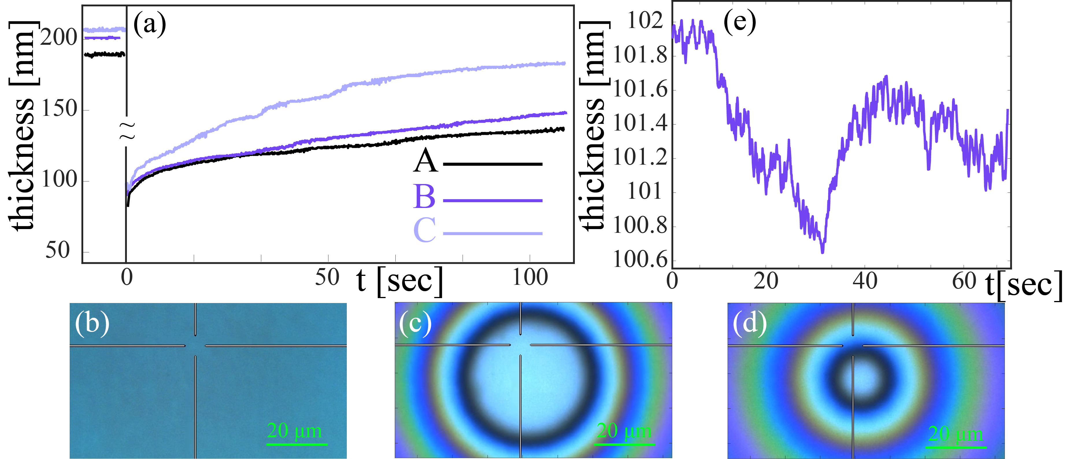
Notably, the thickness change of the silicone oil film occurs at a subnanometer scale but still over a long period of time, which is on the order of seconds. This large characteristic healing time scale allows ruling out other thermally driven effects, such as the thermo-optical effect, which is governed by heat diffusion processes and therefore operates on a much shorter time scale on the order of magnitude of several microseconds (see Supplementary Material). Moreover, even for the case where the thermo-optical effect has a nonnegligible effect, it would still be much smaller than the corresponding contribution due to TLD film deformation driven by the TC effect under identical optical power rubin2018nonlocal .
IV.3 Real-space imaging
Fig.5 presents the experimental results of TLD film equal-height contour lines as well as the corresponding interpolated topography maps. In particular, it shows an indentation formed under focused illumination in a small region with a diameter of approximately m (Fig. 5(a,c)) and a droplet formed under a ring-shaped region with an inner diameter of approximately m (Fig. 5(b,d)). These optically induced heat patterns, which lead to different fluidic patterns, are qualitatively captured by numerical simulation of the corresponding cases presented in Fig. 5(e,f).
The dark resonant contours presented in Fig. 5(a,b) correspond to different equal-height contours of the TLD film free surface, obtained by sweeping the corresponding incident angles and capturing the reflected light from the sample. The step in the illumination angle sweep is per step, and then for each value of the resonant coupling angle we used the theoretical curve to determine the thickness of the silicone oil film.
After the heating beam is switched off, the thin film healing rate is relatively fast, as could also be observed via -space imaging in Fig. 4(a) just after s. The latter implies that real-space imaging of dynamical processes is applicable to processes on time scales smaller than the time scale required to scan the relevant angles. In the present setup, the scanning time was s; this consideration dictated performing the angle scan at later times, characterized by a slower healing process, where the droplet already coalesced with the surrounding thin film.
It is instructive to mention that the curvature of the TLD film in our experiments was sufficiently low, and therefore, its effect on the coupling angle is negligible. Indeed, as seen from Fig. 5(c), the mean slope is approximately m , which is smaller than the critical value predicted by the analysis from Fig. S2(c,d) (see Supplemental Material for details).
IV.4 Effect of thin film periodic undulation on the coupling angle
We now analyze the effect of possible periodic undulation of the TLD film surface due to an uneven subwavelength coupling grating (see Fig. 6(a)) on the resonant coupling angle. The governing equation for the thickness of a thin Newtonian liquid film (note that the silicone oil employed in our experiments is a Newtonian fluid) under the effects of surface tension and centrifugal forces due to rotation with angular velocity is given by stillwagon1990leveling
| (6) |
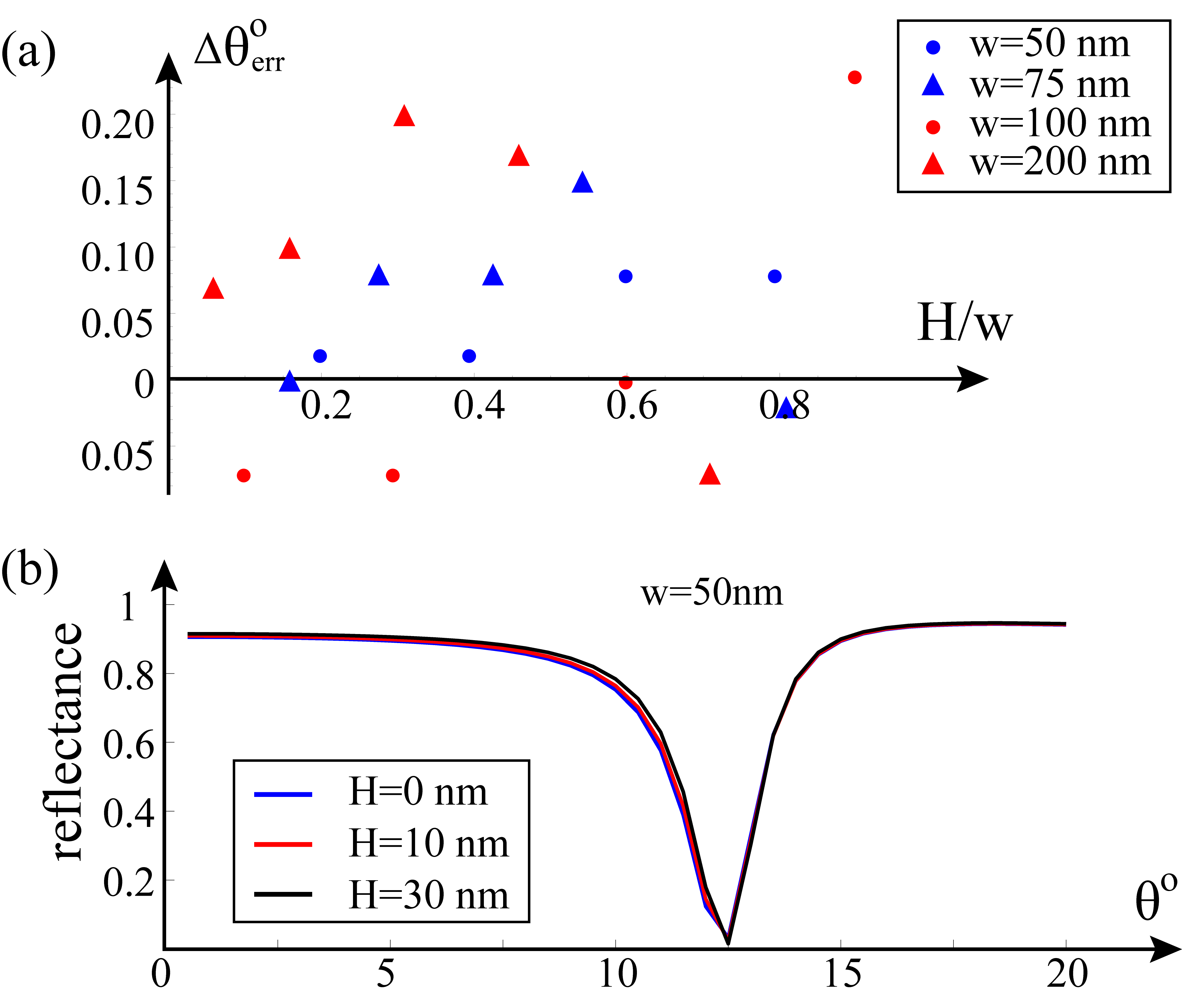
where , and a similar equation with holds over grooves. Here, represents film thicknesses above a grating of depth , is the distance from the rotation axis, and represents a dimensionless ratio of centrifugal to capillary forces. Inserting the following parameters relevant to our system: kg m-3, s-1, m, m, N m-1, and m, into the definition of given by Eq.(9), we learn that . The latter implies that the conditions in our system correspond to a surface-tension-dominated regime, which leads to a practically planar fluid-gas interface (see wu1999complete for a case where ). Indeed, we find that TLD films of thickness values in the range between nm and nm acquire a peak-to-peak undulation depth , on the order of in units of , i.e., much smaller than nm (see Supplementary Material for more details). Nevertheless, we note that higher values of can, in principle, emerge under different experimental conditions that are not met in our work, such as higher values of or cases where non-Newtonian fluids or complex fluids with volatile components (e.g. polymers or photoresists) are employed rawlings2015accurate . Fig. 6(b) presents numerical simulation results of the error in the TLD film thicknesses nm due to the presented values of the undulation peak-to-peak amplitude (in units of ). Interestingly, even large values of lead to a very small shift in the resonant coupling angle. For instance, for the case where nm and nm (which is of the mean thickness), an error is introduced around nm, which corresponds to only of the mean thickness (see Supplemental Material for more details). Importantly, combining the small error introduced by the symmetric undulation amplitude with the analysis above indicating that is expected to be smaller than one nm, we learn that the corresponding value of is expected to be much smaller than one nm even in the presence of a nm deep grating.
V Discussion
In this work we presented dynamical optical patterning of a TLD film and two novel plasmonic methods for the measurement of its thickness and topography, which were applied to determine the film dynamics after being driven out of equilibrium by an optically induced TC effect. In particular, we leveraged the TC effect as a novel heat-based mechanism to induce tuning of the plasmonic resonances. The imaging methods presented in our work are complementary in the sense that while -space imaging provides thickness values as a function of time in a small region, real-space imaging is applicable to a larger area of a few hundreds of microns. Both methods admit immediate generalizations that can be utilized to probe specific fluidic processes by introducing higher-speed sweeping mechanisms (e.g., translation stages) and higher frame-rate cameras; -space imaging can be extended to provide thickness information along spatial segments that can cover 2D regions, whereas real-space imaging can, in principle, capture faster processes that evolve over smaller characteristic times. Our methods open a door for future studies where thickness changes of the TLD film monitored at a subnanometer scale would be indicative of various physical processes, such as thermocapillary instabilities in polymer molten films mcleod2011experimental and instabilities due to electrohydrodynamic schaffer2001electrohydrodynamic and electrostatic morariu2003hierarchial effects. In addition, the methods are applicable to studying pore nucleation ilton2016direct , phase transitions in thin polymer films wallace1995influence and light-induced reversible thickness changes of photosensitive materials yager2006photomechanical without the need to employ, respectively, X-ray reflectivity and neutron reflectometry methods. Importantly, our methods are not compromised if an additional thin layer of solid dielectric is deposited on top of the metal grating to achieve desired surface properties, which, in principle, allows studying basic problems such as the wetting and spreading of thin films on different substrates. Our analysis of the effect of fluid-gas interface periodic undulation on the resonant coupling angle, due to possible interaction with a nonuniform topography (metal grating), showed that it introduces a negligible error in the predicted thickness values. Nevertheless, periodic undulation could be of importance in future studies involving non-Newtonian fluids with volatile components (e.g., polymers) where the peak-to-peak undulation depth may be larger and asymmetrical. Furthermore, we demonstrated a novel optical method/process to create and translate droplets directly from a TLD film, which merits further investigation from a fluid dynamical perspective and may also be useful for future applications in microscopy/nanoscopy lee2009near , where each droplet can serve as a smooth, tunable and mobile micro/nanolens, and in bio-oriented applications in microfluidics. In fact, since the temperature increase required to form the droplets from the liquid is expected to be only a few degrees or less (see Supplemental Material), we expect that our method may be suitable for various applications in the biosciences, such as single virus communication and PCR (polymerase chain reaction) assays, where compartmentalization of the TLD film into an array of droplets may be useful to invoke independent biomolecular reactions kelley2014advancing . We hope that our work, which brings together plasmonic effects, SPRM and fluid dynamics, will stimulate future development of specific optical systems aimed at studying TLD film processes and light-fluid interactions. In particular, other prominent SPRM variants that can be employed include the classical Kretschmann configuration to study the dynamics of TLD films of thicknesses below the grating depth, the holographic-based method mandracchia2015surface , which offers the possibility of simultaneous detection of reflectivity and phase changes in SPR images, and SPP confocal interferometry pechprasarn2014ultrastable , which offers superior noise performance and can improve the lateral resolution.
Materials and Methods
For the TLD film substrate which supports SPP excitations we emloyed gold gratings with a period of nm, % duty cycle, and with nm depth grooves which were fabricated by nanoimprint pattern transfer and lithography. Using electron-beam evaporation, a silicon substrate was layered with nm of Ti as adhesion and nm of Au to form the grating bulk material. A nanoimprint resist bilayer was spun and soft-baked on top with nm of PMMA forming the underlayer and nm of upper layer resist (AR-UVP), onto which a polymeric mold containing the grating features was aligned and stamped while curing the imprinted resist (EVG aligner). After mold/sample separation, reactive ion etch (RIE) recipes were used to remove residual top and bottom layer resists within the pattern trenches. The pattern was transfered from imrpint resist to a metal mask by nm of Cr deposition and acetone liftoff. Using the Cr mask, an additional RIE recipe was used to directly remove nm of Au within the exposed trenches, followed by wet etch removal of Cr. The pattern depth, duty cycle, and periodicity were confirmed by AFM measurements (Nanonics).
For droplet generation in white light imaging setup we used mm diameter Axicon (Thorlabs AR coated UC fused silica) with deflection angle of and with reflectence less than % in the range - nm.
To form a TLD film, silicone oil (Fisher Scientific) of refractive index was spun onto the grating by repeated intervals of spin coating at rpm. Baseline thickness of the prepared fluid film was measured by spectral reflectance to be on average nm by a separate optical profilometer (Filmetrics F20). A complete spin curve for each spin being min in duration, was obtained to prepare baseline average fluid thickness from to nm.
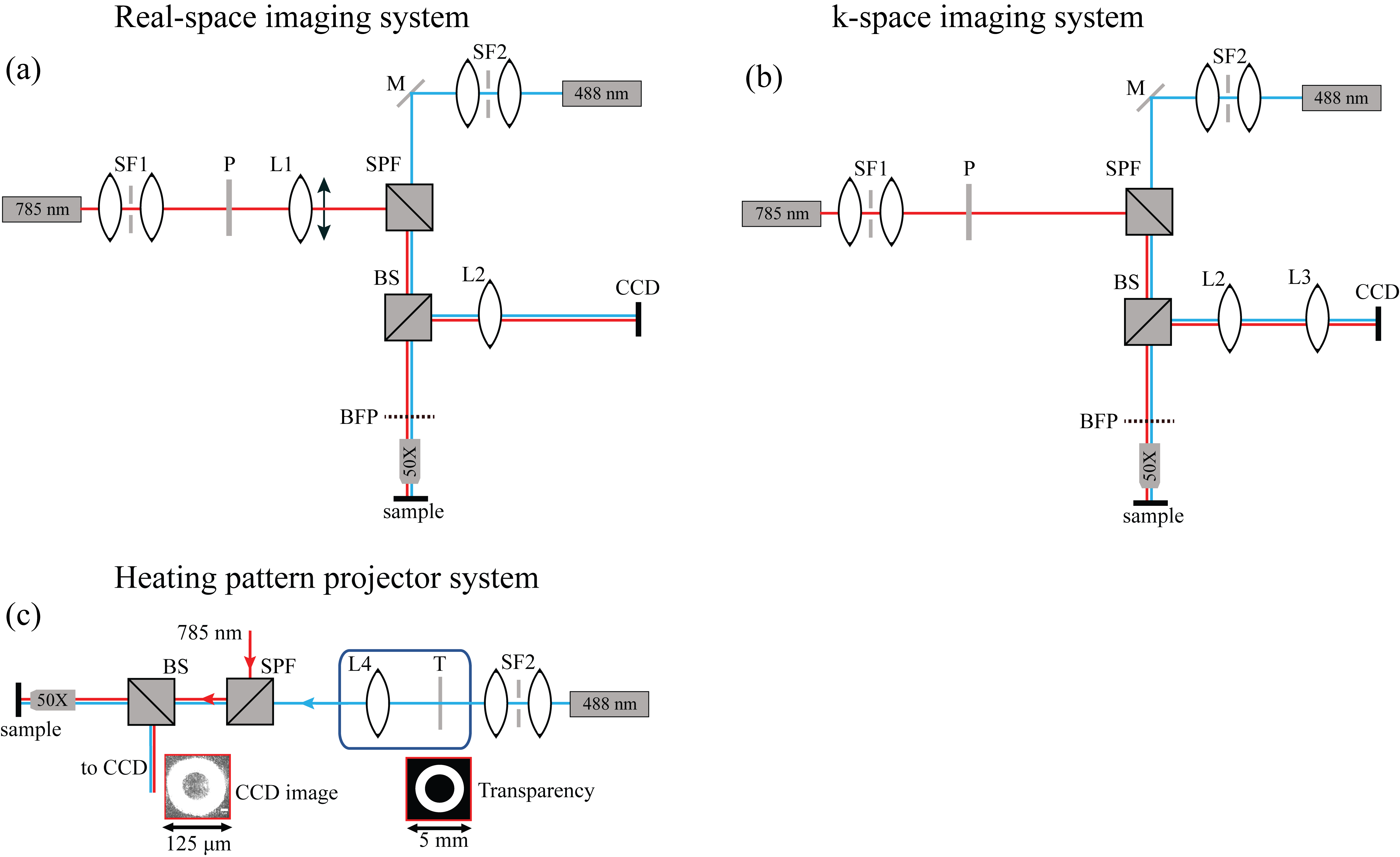
The two complementary imaging modalities we employed in this work, i.e. real-space imaging and k-space imaging employ a very similar optical design described by Fig.S4 in Supplementary Material. In both imaging methods the low power nm probing-beam and the higher power nm heating-beam, were brought to the same optical path by means of a short pass filter (SPF). Upon reflection from the sample, the light was imaged to CMOS camera by utilizing a 50:50 beam splitter (BS). Common to both imaging techniques is microscope imaging system with long working distance 50X objective and internal tube lens. The real-space imaging is accomplished by placing the CMOS camera at the focal plane of the tube lens. For k-space imaging we employed additional lens in order to image the BFP (see Supplementary Material for more details). The standard figure of merit for sensitivity definition is to take it as three times of sigma, where sigma is defined as the standard deviation of the signal. In our case it is natural to compute sigma as the standard deviation of the fluctuating signal as a function of time, with the heating beam switched-off and the probing beam is switched-on; direct computation yields sigma equal to nm and the resultant sensitivity is then nm.
Funding Information
This work was supported in part by the National Science Foundation (NSF), the Office of Naval Research (ONR), the Semiconductor Research Corporation (SRC), the Army Research Office (ARO), DARPA, Cymer Corporation, and the San Diego Nanotechnology Infrastructure (SDNI) supported by the NSF National Nanotechnology Coordinated Infrastructure (grant ECCS-1542148).
Supplemental Documents
See Supplement Material attached below.
References
- (1) R. V. Craster and O. K. Matar, ”Dynamics and stability of thin liquid films,” Rev. Mod. Phys. 81 1131, (2009).
- (2) A. Oron, S. H. Davis, and S. G. Bankoff, ”Long-scale evolution of thin liquid films,” Rev. Mod. Phys. 69 931, (1997).
- (3) J. B. Grotberg, ”Respiratory fluid mechanics and transport processes,” Annu. Rev. Biomed. Eng. 3 421-457, (2001).
- (4) R. Yerushalmi-Rozen, J. Klein, and L. J. Fetters, ”Suppression of rupture in thin nonwetting liquid films,” Science 263.5148 793-795, (1994).
- (5) W. Senaratne, L. Andruzzi, and C. K. Ober, ”Self-assembled monolayers and polymer brushes in biotechnology: current applications and future perspectives,” Biomacromolecules 6 2427-2448, (2005).
- (6) H. Raether, Surface Plasmons on Smooth and Rough Surfaces and on Gratings. (Springer-Verlag Berlin, 2013).
- (7) B. Rothenhäusler and W. Knoll, ”Surface plasmon microscopy,” Nature 332.6165 615, (1988).
- (8) J. W. Sadowski, I.K.J. Korhonen, and J.P.K. Peltonen, ”Characterization of thin films and their structures in surface plasmon resonance measurements,” Optical engineering 34 2581-2587, (1995).
- (9) S. Löfås, M. Malmqvist, I. Rönnberg, E. Stenberg, B. Liedberg, and I. Lundström, ”Bioanalysis with surface plasmon resonance,” Sens. Actuators B Chem. 5 79-84, (1991).
- (10) J. Homola (editor): Surface Plasmon Resonance Based Sensors, Springer, (2006).
- (11) K. Watanabe, K. Matsuura, F. Kawata, K. Nagata, J. Ning, and H. Kano, ”Scanning and non-scanning surface plasmon microscopy to observe cell adhesion sites,” Biomed. Opt. Express 3 354, (2012).
- (12) V. G. Levich, Physicochemical Hydrodynamics (Prentice hall, 1962).
- (13) S. R. C. Vivekchand, C. J. Engel, S. M. Lubin, M. G. Blaber, W. Zhou, Y. J. Suh, G. C. Schatz, and T. W. Odom, ”Liquid plasmonics: Manipulating surface plasmon polaritons via phase transitions,” Nano Lett 12.8 4324-4328, (2012).
- (14) S. Rubin and Y. Fainman, ”Nonlocal and Nonlinear Surface Plasmon Polaritons and Optical Spatial Solitons induced by the Thermocapillary Effect,” Phys. Rev. Lett. 120, 243904 (2018).
- (15) B. Huang, F. Yu, and R. N. Zare, ”Surface plasmon resonance imaging using a high numerical aperture microscope objective,” Anal. Chem. 79 2979, (2007).
- (16) J. P. Singer, S. E. Kooi, and E. L. Thomas, “Focused laser-induced marangoni dewetting for patterning polymer thin films,” J. Polym. Sci. B. 54.2 225-236, (2016).
- (17) J. P. Singer, ”Thermocapillary approaches to the deliberate patterning of polymers,” J. Polym. Sci. B 55 1649-1668, (2017).
- (18) J. H. Yoo, J. B. In, C. Zheng, I. Sakellari, R. N. Raman, M. J. Matthews, and C. P. Grigoropoulos, “Directed dewetting of amorphous silicon film by a donut-shaped laser pulse,” Nanotechnology 26(16) 165303, (2015).
- (19) W. Han, L. Jiang, X. Li, Q. Wang, S. Wang, J. Hu, and Y. Lu, “Controllable plasmonic nanostructures induced by dual-wavelength femtosecond laser irradiation,” Sci Rep. 7(1) 17333, (2017).
- (20) P. Zhu and L. Wang, ”Passive and active droplet generation with microfluidics” Lab on a Chip. 17 34-75, (2017).
- (21) C. N. Baroud, J. P. Delville, F. Gallaire, and R. Wunenburger, ”Thermocapillary valve for droplet production and sorting,” Phys. Rev E. 75 046302, (2007).
- (22) P. Kvasnička and J. Homola, ”Convenient Method of Micrometer-Scale Excitation of Propagating Surface Plasmons by a Focused Laser Beam,” Plasmonics 9 737-739, (2014).
- (23) G. Bartal, O. Cohen, H. Buljan, J. W. Fleischer, O. Manela, and M. Segev, “Brillouin zone spectroscopy of nonlinear photonic lattices,” Phys. Rev. Lett. 94 163902, (2005).
- (24) L. S. Jung, C. T. Campbell, T. M. Chinowsky, M. N. Mar, and S. S. Yee, “Quantitative Interpretation of the Response of Surface Plasmon Resonance Sensors to Adsorbed Films,” Langmuir, 14.19 5636, (1998).
- (25) P. B. Johnson and R. W. Christy, ”Optical constants of the noble metals,” Phys. Rev. B 6 4370, (1972).
- (26) E. F. Aust, M. Sawodny, S. Ito, and W. Knoll, ”Surface plasmon and guided optical wave microscopies,” Scanning 16 353-362, (1994).
- (27) L. Pang, K. A. Tetz, and Y. Fainman, ”Observation of the splitting of degenerate surface plasmon polariton modes in a two-dimensional metallic nanohole array,” Appl. Phys. Lett. 90 111103, (2007).
- (28) T. Holmgaard and S. I. Bozhevolnyi, ”Theoretical analysis of dielectric-loaded surface plasmon-polariton waveguides,” Phys. Rev. B. 75 245405, (2007).
- (29) H. Kogelnik and V. Ramaswamy, ”Scaling rules for thin-film optical waveguides,” Appl Opt. 13 1857-1862, (1974).
- (30) H.M.J.M. Wedershoven, C.W.J. Berendsen, J.C.H. Zeegers, and A.A. Darhuber, ”Infrared laser induced rupture of thin liquid films on stationary substrates,” Appl. Phys. Lett. 104 054101, (2014).
- (31) L. E. Stillwagon and R. G. Larson, “Leveling of thin films over uneven substrates during spin coating,” Phys. Fluids 2 1937, (1990).
- (32) P. Y. Wu and F.‐C. Chou, “Complete analytical solutions of film planarization during spin coating,” J. Electrochem. Soc. 146 3819, (1999).
- (33) C. Rawlings, H. Wolf, J. L. Hedrick, D. J. Coady, U. Duerig, and A. W. Knoll, ”Accurate location and manipulation of nanoscaled objects buried under spin-coated films,” ACS nano 9 6188, (2015).
- (34) E. McLeod, Y. Liu, and S. M. Troian, ”Experimental verification of the formation mechanism for pillar arrays in nanofilms subject to large thermal gradients,” Phys. Rev. Lett. 106 175501, (2011).
- (35) E. Schöffer, T. Thurn-Albrecht, T. P. Russell, and U. Steiner, ”Electrohydrodynamic instabilities in polymer films,” EPL 53 518, (2001).
- (36) M. D. Morariu, N. E. Voicu, E. Schöffer, Z. Lin, T. P. Russell, and U. Steiner, ”Hierarchical structure formation and pattern replication induced by an electric field,” Nat. Mater. 2 48, (2003).
- (37) M. Ilton, C. DiMaria, and K. Dalnoki-Veress, “Direct measurement of the critical pore size in a model membrane,” Phys. Rev. Lett. 117.25 257801, (2016).
- (38) W. E. Wallace, J. H. Van Zanten, and W. L. Wu, Influence of an impenetrable interface on a polymer glass-transition temperature. Phys. Rev. E. 52 R3329, (1995).
- (39) K. G. Yager, O. M. Tanchak, C. Godbout, H. Fritzsche, and C. J. Barrett, “Photomechanical effects in azo-polymers studied by neutron reflectometry,” Macromolecules 39 9311-9319, (2006).
- (40) J. Y. Lee, B. H. Hong, W. Y. Kim, S. K. Min, Y. Kim, M. V. Jouravlev, R. Bose, K. S. Kim, I. C. Hwang, L. J. Kaufman, and C. W. Wong, ”Near-field focusing and magnification through self-assembled nanoscale spherical lenses,” Nature 460.7254 498, (2009).
- (41) S. O. Kelley, C. A. Mirkin, D. R. Walt, R. F. Ismagilov, M. Toner, and E. H. Sargent, ”Advancing the speed, sensitivity and accuracy of biomolecular detection using multi-length-scale engineering,” Nat. Nanotechnol. 9 969, (2014).
- (42) B. Mandracchia, V. Pagliarulo, M. Paturzo, and P. Ferraro, “Surface plasmon resonance imaging by holographic enhanced mapping,” Anal. Chem. 87(8) 4124, (2015).
- (43) S. Pechprasarn, B. Zhang, D. Albutt, J. Zhang, and M. Somekh, ”Ultrastable embedded surface plasmon confocal interferometry,” Light: Science & Applications 3(7) e187, (2014).
SI
Supplemental Material for
“Subnanometer imaging and controlled dynamical patterning of thermocapillary driven deformation of thin liquid films”
Shimon Rubin, Brandon Hong and Yeshaiahu Fainman
Department of Electrical and Computer Engineering, University of California, San Diego, 9500 Gilman Dr., La Jolla, California 92023, USA
S.1 Momentum conservation diagrams
Fig. S1 presents schematic description of the momentum conservation relation, given by Eq.3 in the main text.
The latter, describes coupling of an incident light into SPP mode of momentum which allows to deduce the corresponding resonant coupling angle . In particular, employing Eq.5 in the main text as well as the mutual orientation of the emerging two dark resonant arcs, allows to determine by experimental measurement of the distance between the arcs. For films thinner than the critical thickness , the emerging resonant dark arcs, point towards each other (Fig. S1(b)), whereas for thicker films, i.e. for , the dark arcs point in the opposite directions. Furthermore, while in the regime the in-plane component of an incident free-space mode is anti-parallel to (), the regime is characterized by and SPP mode momentum which is parallel to the in plane component of an incident plane-wave momentum. Importantly, some cases, such as the nm probing-beam case described in Fig. 2(g) in the main text, do not admit critical height . Consequently, the relative orientation of the emerging dark arcs in such cases is oriented towards each other for all thickness values. For sufficiently thick film, above a WG threshold condition, the dielectric film and the metal grating support also resonant coupling into WG modes. The corresponding resonant angle diagrams would then admit an additional pair of dark arcs (one pair for each higher-order WG mode) on top of the resonant dark arcs associated with the SPP mode. Small thickness perturbations of such thick films would lead to changes of the WG dark arcs whereas the SPP resonant curves would not change as could be also anticipated from the low sensitivity regions of SPP curves at high film thicknesses, presented in Fig. 2 in the main text.
S.2 Underlying main assumptions of Eq.5
The free surface of a Newtonian liquid film of viscosity and stress tensor satisfies the following stress balance equation oron1997longSM
| (1) |
where, is the surface tension, stands for a gradient with respect to the in-plane coordinates () and is the 3D divergence of the unit vector normal to the film surface. Assuming the surface tension depends linearly on the temperature via , applying lubrication approximation for the Navier-Stokes equation, taking the thin film limit of the matching conditions on the fluid-gas interface oron1997longSM , and assuming quasi-static temperature field distribution, yields rubin2018nonlocalSM
| (2) |
The minus (positive) sign of the source term in Eq.(2) indicates decrease (increase) of local thickness for positive (negative) Marangoni constant. Scaling to dimensionless variables via where , , and yields
| (3) |
where is the dimensionless Marangoni number.
The heat diffusion equation that governs the temperature field, , on a metal substrate with heat diffusivity is
| (4) |
The latter implies that the maximal temperature arise, , due to a circular laser beam of intensity and waist , is subject to
| (5) |
where is the optical absorption coefficeint. For a low power beam of intensity Wm-2 and heat conductivity of gold, which is around Wm-1K-1, reflectance at nm and m, the corresponding K.
S.3 Derivation of Eq.6
The governing equation for the axisymmetric flow of a TLD Newtonian film under the effects of surface tension and centrifugal force due to rotation of the substrate with axisymmetric roughness, and furthermore under lubrication approximation is given by stillwagon1990levelingSM
| (6) |
Here, is the radial coordinate, is the fluid density, is the angular velocity, is the local TLD film thickness relative to the topographic feature and is the local substrate height, so is the local height of the fluid-gas interface relative to the substrate. Switching to dimensionless variables via
| (7) |
where represents fluid thickness above the grating ridge and is the time scale based on the centrifugal force, and furthremore dropping the time derivative yields the following time independent equation for dimensionless thin film thickness stillwagon1990levelingSM
| (8) |
where represents a dimensionless ratio of centrifugal to capillary forces. Here, dropping the time derivative is justified because the characteristic time for the film thinning process, , is much larger than that for the rotational flow , and therefore we can expect the film profile over the grating to adjust to changes in the overall film thickness at a rate much faster than the overall film thickness itself changes stillwagon1990levelingSM . In fact, in our system m, m and . Treating to as a piece-wise constant function, and linearizing Eq.(8) above the grating ridge and trench via and , respectively, we can omit the derivative of leading to stillwagon1990levelingSM
| (9a) | |||
| (9b) | |||
S.4 Details of numerical simulation
Geometry: The scheme of the simulation domain is presented at Fig. 1 in the main text and it resides in the region m m and m m. The metal substrate resides in the region between m m and it hosts another nm depth metal grating stripe in the region m m (i.e. half-duty cycle) and m m.
Computational domain: The computational grid accommodates and elements along the - and -axis, respectively. While the spacing between numerical grid points is uniform along the -axis, the grid is non-uniform along the - axis. The latter admits a finer mesh near the metal surface, accommodating elements in the region near the metal surface, m. The implemented boundary conditions are Bloch along -axis and PML along and axes. PML settings: stretched coordinate PML; min layer: 12; max layers: 64; kappa=3; sigma=1.5; polynomial:3; alpha=0; alpha polynomial:1.
Dielectric properties: For incident plane wave of wavelength nm and nm, the corresponding dielectric constant of gold is and , respectively johnson1972opticalSM . The refractive index of the thin film is , which corresponds to refractive index of silicone oil employed in our experiments.
Source and monitor: The source is a plane wave injected at m at different angles, typically between and relative to the axis. The monitor collects the reflected wave at m.
S.5 Numerical results of an angular band-gap and the effect of thin film’s curvature on the resonant coupling angle
Increasing the dielectric thickness on top of the metal grating from zero thickness (i.e. no dielectric) to higher values, leads to a monotonic increase of the coupled SPP wavevector, and therefore results in an increasingly smaller resonant coupling angle. In some cases where the coupling angle at is sufficiently low, the dielectric angular band-gap opens around the normal incidence angle at critical thickness , which results in a lower coupling efficiency into SPP mode. Fig. S2 below, describes coupling of a TM polarized nm plane-wave into SPP mode on gold grating (grating period nm) with an angular bandgap around critical thickness nm (Fig.S2(b)).
We would like to probe the effect of local non-homogeneity in TLD film thickness, on the value of the corresponding resonant coupling angle to the SPP mode. To this end, we construct a numerical simulation domain of width , schematically presented in Fig. S2c, and employ a commercial-grade simulator based on the finite-difference time-domain method (Lumerical, FDTD). The shape of the non-homogeneity is taken as an indentation of a Gaussian form, with a width parametrized by via
| (10) |
Fig. S2d presents numerical results of the corresponding resonant angle as a function of indentation width for a fixed Gaussian source beam, , of width at half maximum . In the limit of increasingly wider indentations, described by , the coupling angle tends to the resonant angle that corresponds to a flat dielectric of thickness , whereas in the opposite limit of narrower indentations (), the coupling angle tends to the resonant angle that corresponds to a flat dielectric of thickness . In particular, we learn that for increasingly smaller the coupling angle experiences a significant shift only at sufficiently sharp indentations that introduce a mean slope around the value .
S.6 Numerical simulation details in Fig.4
Numerical integration of Eq.(3) is accomplished by utilizing commercial grade numerical solver (Mathematica, v. 11) and implementing its built-in Explicit Runge Kutta method. The size of the simulation domain in dimensionless units along the and directions is , and the deformation is subject to a vanishing boundary conditions on the lines . The spacing of the numerical grid is 0.3 and the number of effective digits of precision is three. The dimensionless number is taken as unity. The intensity, , is taken as , where corresponds to maximal temperature and thinning at the origin, whereas corresponds to maximal temperature and thinning on a circle of radius , which leads to a drop-like structure.
S.7 Comparison of sensitivities to thickness changes due to Fresnel reflection and coupling into SPP
Consider the value of the ratio , defined as where is the change of reflectivity due to the corresponding change of TLD film thickness and is the change of thickness whereas. For Fabry-Perrot (FP) and SPP modes, the maximal value of the ratio is given by and , respectively. Here, is the change of the dielectric thickness that corresponds to a maximal shift of reflectivity given by where is the Fresnel normal reflection coefficient; is the change of thickness which corresponds to twice the width of the angular half-width depth, , of the corresponding resonance angle -thickness curve. Assuming , and furthermore utilizing the values , , nm, and the corresponding nm, yields enhancement of the proposed method by .
S.8 Shape of thin liquid film under spinning on a substrate with periodic topography
Following wu1999completeSM , the corresponding solution of the governing equation (Eq.(14) in the main text) of TLD film under capillary and centrifugal forces in the quasi-static limit is given by the linear superposition of the functions
| (11) |
Here, denote regions above the grating trench and ridge, respectively, and the corresponding functions are given by
| (12) |
where take the following values in each one of the domains
| (13) |
The corresponding coefficients , , are then determined by the continuity of the fluid-air height as well as its first and second derivatives at points and .
Inserting the value derived below Eq.(14) in the main text, we find that under surface tension and centrifugal forces the following values of mean thickness nm lead to the following values of , , , in units of , i.e. much smaller than nm.
S.9 Numerical results of the effect of thin film’s undulation on the value of the resonant coupling angle
Let us determine the effect of thin film undulation derived above, on the value of the resonant coupling angle. To this end we perform numerical simulations of an incoming plane wave on a grating of period described in Fig. 4(a) in the main text. The corresponding shift in the resonant angle is described in Fig. S3a. Remarkably, the corresponding angle shift is a very weak function of , even for values of comparable to . Fig. S3b furthermore indicates that the reflectance curve is practically unaffected by the periodic symmetric undulation. Periodic undulations which are not symmetric relative to the grating are expected to modify the resonant coupling angle for sufficiently large amplitude, and these are not considered in this work.
S.10 Experimental setup, fabrication details, and sample preparation
Fig.S4 presents the schematic description of the optical setup we employed in our experiments. In particular, Fig.S4a and Fig.S4b describe the experimental setups we used for real-space and -space measurements, respectively, whereas Fig. S4c presents the pattern projection setup. The low power near infra-red (NIR) laser diode ( nm) is used as a probing-beam, whereas the higher power argon laser ( ) nm is used as a heating-beam; these two beams were brought to the same optical path by means of a short pass filter (SPF). Upon reflection from the sample, the light was imaged to CMOS camera by utilizing a 50:50 beam splitter (BS). Real-space imaging is achieved by placing the camera in the the back focal plane (BFP) of the tube lens, and by placing an additional lens L1 in the illumination path of the probing beam in order to deliver a plane wave to the sample; L1 is mounted on a translation stage which can change its position in a direction perpendicular to the optical axis. -space imaging is achieved by inserting lens L3 after lens L2 in order to complete a 4f imaging system to image the BFP of the microscope objective, and by removing lens L1 in order to focus the probing beam onto the sample. The heating pattern projector unit described in Fig. S4c, is comprised of a transparency mask and an additional 15 inch lens L4 placed before SPF. For droplet generation in white light imaging setup we used mm diameter Axicon (Thorlabs AR coated UC fused silica) with deflection angle of and with reflectence less than % in the range - nm, and heating beam which employs mW laser power source of wavelength nm.
For the metal substrate which supports SPP excitations and hosts TLD film we employed a % duty cycle gold grating of nm period and with nm depth grooves which were fabricated by nanoimprint pattern transfer and lithography, as described below. Using electron-beam evaporation, a silicon substrate was layered with nm of Ti as adhesion and nm of Au to form the grating bulk material. A nanoimprint resist bilayer was spun and soft-baked on top with nm of PMMA forming the underlayer and nm of upper layer resist (AR-UVP), onto which a polymeric mold containing the grating features was aligned and stamped while curing the imprinted resist (EVG aligner). After mold/sample separation, reactive ion etch (RIE) recipes were used to remove residual top and bottom layer resists within the pattern trenches. The pattern was transfered from imrpint resist to a metal mask by nm of Cr deposition and acetone liftoff. Using the Cr mask, an additional RIE recipe was used to directly remove nm of Au within the exposed trenches, followed by wet etch removal of Cr. The pattern depth, duty cycle, and periodicity were confirmed by AFM measurements (Nanonics).
To form a TLD film, silicone oil (Fisher Scientific) of refractive index was spun onto the grating by repeated intervals of spin coating at rpm. Baseline thickness of the prepared fluid film was measured by spectral reflectance to be on average nm by a separate optical profilometer (Filmetrics F20). A complete spin curve for each spin being min in duration, was obtained to prepare baseline average fluid thickness from to nm.
S.11 Movie demonstrating -space thickness measurement of TLD film
Experimental -space imaging results, demonstrating dynamical nanometric thickness change of thin silicone oil film as a function of time due to optically-driven TC effect and the following healing dynamics after the illumination source is switched off. Top, presents the resonant angles along the central line of the -space diagram, whereas bottom present the corresponding thickness at the illuminated small region, nearly of minimal size allowed by diffraction.
References
- (1) A. Oron, Alexander, S. H. Davis, and S. G. Bankoff, ”Long-scale evolution of thin liquid films,” Rev. Mod. Phys. 69 931, (1997).
- (2) S. Rubin and Y. Fainman, ”Nonlocal and Nonlinear Surface Plasmon Polaritons and Optical Spatial Solitons induced by the Thermocapillary Effect,” Phys. Rev. Lett. 120 243904, (2018).
- (3) L. E. Stillwagon and R. G. Larson, ”Leveling of thin films over uneven substrates during spin coating,” Phys. Fluids 2 1937, (1990).
- (4) P. B. Johnson and R. W. Christy, ”Optical constants of the noble metals,” Phys. Rev. B 6, 4370 (1972).
- (5) P. Y. Wu and F.‐C. Chou, ”Complete analytical solutions of film planarization during spin coating,” J. Electrochem. Soc. 146.10 3819, (1999).