Influence of nanostructuring on silicon vacancy center spins in diamond pillars
Abstract
Color centers in diamond micro and nano structures are under investigation for a plethora of applications. However, obtaining high quality color centers in small structures is challenging, and little is known about how properties such as spin population lifetimes change during the transition from bulk to micro and nano structures. In this manuscript, we studied various ways to prepare diamond samples containing silicon vacancy centers and measured how population lifetimes of orbital states change in pillars as we varied their dimensions from approximately 1 m to 120 nm. We also researched the influence of the properties of the diamond substrate and the implantation and annealing methods on the silicon vacancy inhomogeneous linewidth and orbital lifetime. Our measurements show that nominally identical diamond samples can display significantly distinct inhomogeneous broadening. We observed weak indications that restricted vibrational modes in small structures may extend population lifetimes. However, imperfections in the crystal lattice or surface damage caused by etching reduce population lifetimes, especially in the smallest structures.
Color centers in diamond are used for a broad variety of applications such as sensing Maze et al. (2008), hybrid optomechanical systems Burek et al. (2016); Golter et al. (2016); Lee et al. (2017) and quantum information processing Jelezko et al. (2004); Dutt et al. (2007); Fuchs et al. (2011); Hensen et al. (2015); Childress and Hanson (2013); Atatüre et al. (2018). Many of these applications require color centers implanted Evans et al. (2016); Kehayias et al. (2017) within micro or nano structures Schröder et al. (2016) that are engineered to modify the opticalFujita et al. (2005) or phonon density of states Lutz et al. (2016), and they require color centers that are stable in their emission wavelength. The latter is particularly important in order to use the centers as sources of indistinguishable photons Sipahigil et al. (2014); Marseglia et al. (2018) in quantum networking applications. This also demands that an ensemble of color centers shows narrow inhomogeneous broadening. However, no systematic studies on how the transition from bulk to nano-structures influences spectroscopic properties have been reported for color centers in nanostructured diamond.
Among the numerous diamond color centers, the negatively charged silicon-vacancy center (SiV) has recently received much attention Weinzetl et al. (2019); Sipahigil et al. (2016); Sohn et al. (2018); Wein et al. (2018) due to its favorable spectroscopic properties (Becker et al., 2018) that make it appealing for the above mentioned applications. Its inversion-symmetric potential makes it less susceptible to spectral diffusion compared to the nitrogen-vacancy (NV) center, which exhibits a permanent electric dipole moment. Furthermore, more than 80% of its emission is contained in its zero phonon line (Neu et al., 2011). It was for these reasons that the SiV was selected for the presented studies, however, we believe that the conclusions drawn here may also be relevant for other color centers.
For the experiments presented in this manuscript, we examined SiV color centers created by ion implantation in several diamond samples from the same supplier. We studied differences between the samples and investigated to what degree thermal annealing can alter their properties in terms of inhomogeneous linewidth and lifetime of orbital states. Furthermore, we investigated how the SiV orbital state lifetimes change when their environment is etched to create nano-pillars of varying size. We found that variations between diamond samples, possibly related to strain, can play an important role in obtaining SiV with a narrow inhomogeneous broadening. Re-annealing was not found to be successful in reducing the inhomogeneous broadening of implanted SiVs. Finally, we observed that orbital state lifetimes tend to decrease in the smallest nanostructures rather than increase, due to a suppression of resonant vibrational modes.
All diamond samples studied here were purchased from Element Six and were identical according to their specifications; 330.5 mm electronic grade (typical nitrogen concentration of /cm3 and NV concentration of /cm3) diamond chips, polished on both sides. The low NV concentration is required since the presence of many NVs in the sample can mask the SiV signal. The samples were cleaned using a mixture of perchloric, nitric, and sulphuric acid (1:1:1) heated to 250 (tri-acid solution), followed by a 3:1 mixture of sulphuric acid and hydrogen peroxide (Piranha solution) pre-heated to 90 . After those cleaning steps, silicon ions (28Si+) were implanted into the sample with a dose of ions/cm2 and an energy of 150 keV by Innovion Corporation. This implantation energy was predicted to result in an implantation depth of around 120 nm according to SRIM simulationsZiegler, Ziegler, and Biersack (2010). Subsequently, the samples were cleaned again using the tri-acid solution and then annealed for 12 hours at temperatures up to 1100 and under vacuum ( torr) Evans et al. (2016), followed by another tri-acid cleaning step.
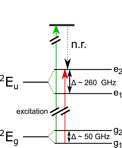
To investigate the effect of nanofabrication on SiV properties, we first characterized SiVs implanted in the bulk samples after implantation and annealing. The relevant electronic level structure of the SiV is shown in Fig. 1. It is composed of the ground () and excited state (). For both, the spin-orbit interaction partially lifts the degeneracy and splits the states into the levels , and , , respectively. Each of those levels further splits under the application of a magnetic field. The SiV features an optical transition at 737 nm (red arrow) that we used for our experiments. The diamond sample was cooled to 5 K using a Montana Instruments closed cycle cryostat (Nanoscale Workstation). A standard homebuilt confocal microscope, described in Hadden et al. (2018), was employed for our spectroscopic measurements and SiV characterization: A long-working-distance microscope objective (NA = 0.5) outside the cyrostat and positioned using a three axis piezo stage was used to focus the excitation sources through the cyrostat top window. A single mode fiber was used as a pinhole to spatially filter the collected photoluminescence. This confocal microscope focused the green laser to a spot size of about 1 m and always excited several color centers at the same time for the implantation density used here. Thus, all our bulk spectra reflect inhomogeneous broadening of the illuminated SiV.
As a first step in SiV characterization, we excited the center incoherently with a 532 nm green laser (green arrow in Fig. 1) and monitored the emission using a spectrometer (Acton SP2750).
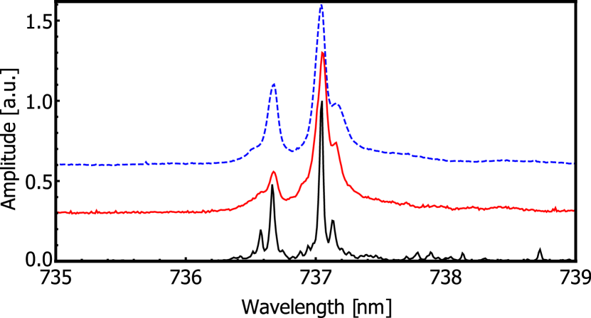
Spectra from three different diamond chips, all produced with the same method, are shown in Fig. 2. Each spectrum shows peaks corresponding to the four expected optical transition lines connecting the two excited states with the two ground states. However, only sample 3 (represented by the black trace) features inhomogeneous broadening narrow enough so that each individual line is clearly resolvable. The resolution of the spectrometer ( 20 GHz) was not sufficient to resolve the contributions of the individual SiV to the inhomogeneous broadening. To obtain high-resolution spectra, we scanned a tunable diode laser (New Focus Velocity TLB-6700) with a linewidth of around 1 MHz across the 737 nm absorption line, and monitored the photoluminescence from the phonon sideband Jahnke et al. (2015). An excerpt of the high-resolution spectrum together with the corresponding part of the low-resolution spectrum from the spectrometer is shown in the inset of Fig. 2.
The spectrum from sample 3 clearly shows contributions from SiVs with different emission wavelengths, likely due to each center experiencing a slightly different crystal environment in terms of residual stress from crystal polishing or implantation (i.e. the line is inhomogeneously broadened). However, since all samples were processed following the same implantation and annealing process, we conclude that the observed differences in inhomogeneous linewidth are likely caused by differences in the original diamond chips.
Since small inhomogeneous broadening is a key figure of merit, we investigated to what degree re-annealing the samples can help to relieve residual stress and reduce the inhomogeneous broadening of the centers. Sample 1 (see Fig. 2) was re-annealed in a home-built vacuum (< torr) tube furnace. The furnace temperature was increased from 20-800 over 6 hours, held at 800 for 4 hours, ramped to 1100 in 4 hours, and held at 1100 for 12 hours. Figure 3 shows the inhomogeneous broadening, averaged over measurements taken from many different spots on the sample, before annealing (red trace) and after annealing (red trace).
There is no observable difference between the spectra before and after annealing. Thus, thermal treatment beyond the initial annealing after ion implantation does not influence the amount of inhomogeneous broadening.
Pre-etching the surface, i.e. removal of the top layer by reactive ion etching to remove any polishing damage, also did not reduce the inhomogeneous broadening.
For applications involving color centers embedded within nanostructures, it is valuable to understand how their properties are affected by the nanofabrication process as well as the resulting geometry. This is particularly interesting for the coupling of color centers to photonic or phononic nanocavities, where predicted enhancements of the colour center’s spin dynamics from locally engineered density of states can be degraded by deleterious effects resulting from etched surfaces and other nanofabrication-induced changes to the material. Ideally, such changes can be minimized through optimized processing, for example by using gentle etching processes Cui (2014) and surface treatments Fu et al. (2010); Chu et al. (2014). To investigate how nanofabrication, and in particular surfaces created using oxygen plasma etching, influences SiV properties, we conducted a study of the lifetime of the upper orbital state (labeled in Fig. 1) of the negatively charged SiV ground state manifold. These measurements were conducted for SiV colour centres in nanostructures with varying dimension, as described below. We performed these experiments on sample 3, which showed the smallest inhomogeneous broadening in the characterization experiments described above.
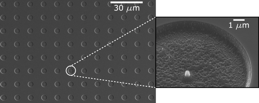
The nanostructure pattern used here to probe the influence of nanofabrication on SiV spin lifetime was an array of nanopillars with diameters varying from 120 to 900 nm and heights of approximately 1 m. The pillars were created using electron beam lithography followed by C4F8/SF6 reactive ion etching to transfer the pillar array pattern to a silicon nitride hard mask deposited on the diamond chip using plasma enhanced chemical vapour deposition (PECVD). An oxygen plasma etch was then used to transfer the pattern to the diamond chip. We followed the same process as described in Khanaliloo et al. (2015) omitting only the final isotropic undercutting step which was not required for these micropillar structures. After etching, the sample was cleaned in hydrofluoric acid solution to remove the SiN, followed by tri-acid and Piranha solutions. A scanning electron microscope image of the resulting nanopillars is shown in Fig. 4.
To measure the lifetimes of the upper orbital state of implanted SiVs in the nanopillars, we optically excited the SiV resonantly on the transition () and monitored the resulting phonon sideband fluorescence as in the resonant excitation measurements from Fig. 2. We first transfered population from the ground state into the upper orbital state via the application of a laser pulse resonant with the transition , which then decayed into either orbital ground state. By pumping long enough ( 80 ns), most population was transferred to state . Due to this population inversion, the fluorescence collected and measured with an avalanche photodiode decreased during the excitation pulse. To extract the lifetime of the state, another 80 ns pulse was applied on the same transition after a wait time . Depending on the wait time and the lifetime of the orbital state, some population relaxed back into ground state , which manifested itself in an increase in fluorescence compared to the steady state fluorescence at the end of the first pulse. The lifetime could then be extracted by fitting an exponential function
| (1) |
to the ratio of the integrated fluorescence signal during first population inversion pulse and the second population inversion (readout) pulse . Here is the maximum observed population inversion fraction. An example spin lifetime measurement of a SiV in a 300 nm pillar is shown in the inset of Fig. 5. Note that under resonant excitation the SiV can change its charge state and subsequently turn dark. However, it is possible to reset a SiV to the negative charge state using excitation at 532 nm Dhomkar et al. (2018); Nicolas et al. . Therefore for every 1000 iterations of the life time measurement (1000 2 80 ns, 37 W, 737 nm cw power) we applied a charge state reset green laser pulse (45 us, 20 W 532 nm cw power).
Using this method, we measured the orbital state lifetime of implanted SiVs in nanopillars of varying diameter and compared it to the result obtained for SiVs in unpatterned regions of the same chip far from the fabricated pillars. The lifetime of the upper orbital state and its dependence on the pillar diameter is shown in Fig. 5 where the bulk lifetime with an uncertainty of 4 ns (due to the averaging of SiVs in different locations within the bulk) is represented as a horizontal line .
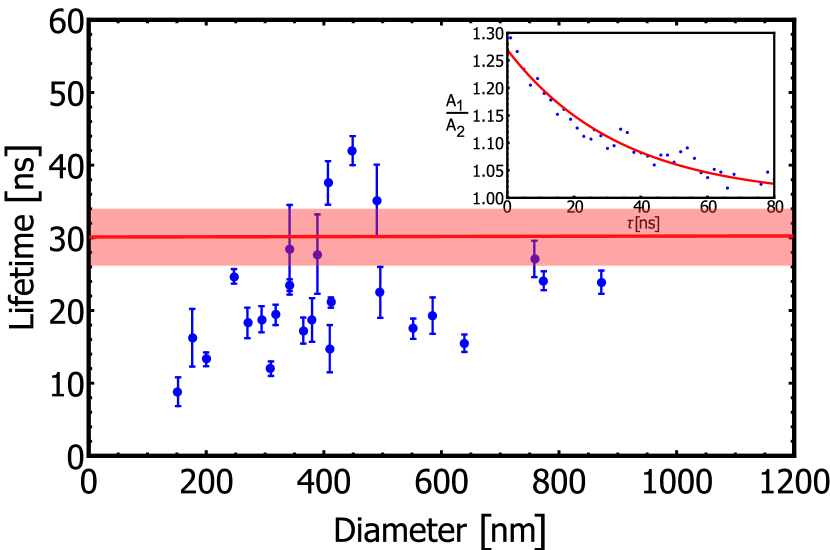
For SiVs in bulk diamond the lifetime of is limited by vibrational modes (phonons) Jahnke et al. (2015) resonant with the transition to the ground state . However, in small structures the density of these modes is expected to decrease Lutz et al. (2016). As the two orbital states that we studied here are spaced by 50 GHz, resonant phonons should be restricted in structures with dimensions smaller than 150 nm. Such a restriction is expected to manifest itself in an increase in the orbital state lifetime.
Our measurements show that the largest pillars possess lifetimes comparable to the bulk. In smaller pillars with diameters around 500 nm, some SiVs exhibit slightly longer lifetimes than the bulk average. This may indeed be a weak signature of an onset of the expected lifetime increase in small structures. However, overall our lifetime measurements show a strong scatter with a decreasing trend for smaller pillar sizes. The strong scatter probably stems from the fact that the measured SiV were not always in the pillar’s center since our pillars were fabricated after SiV implantation without first determining the location of individual SiVs. A SiV located closely to the edge of a large pillar where the crystal lattice is imperfect can thus possess a lifetime comparable to a SiV in the center of a much smaller pillar. We believe that reduced lifetimes are caused by imperfections in the crystal lattice surrounding the SiV, likely created during etching. Thus, to confirm our hypothesis that restricted vibrational modes can extend lifetimes, more data, especially from centers that are deterministically placed in high-quality, small pillars would be needed.
The experiments described in this manuscript show that in order to obtain SiV ensembles with a narrow inhomogeneous broadening it is important to first obtain a high-quality diamond sample with low amounts of residual stress. Even though our diamond samples were nominally identical, two of our three, according to their specifications identical samples displayed a significantly distinct inhomogeneous broadening. Only one sample featured a narrow enough inhomogeneous broadening to resolve the four lines of the SiV. Thus, the available specifications for diamond chips are not sufficient to allow for reproducible SiV fabrication. Re-annealing was not found to be successful in influencing the inhomogeneous linewidth. Furthermore, we found that the orbital state lifetime can be affected by nano-fabrication. For some SiVs in pillars with diameters around 500 nm we find slightly increased lifetimes compared to the bulk that may be due to restriction of vibrational modes. However, the measured lifetimes show strong scatter presumably due to random placement of SiVs within the pillars and for the smallest structures we found a trend towards decreased lifetimes; possibly related to imperfections in the crystal lattice or surface damage caused by etching. To confirm an increase in orbital state lifetime due to the suppression of vibrational modes, more experiments with deterministically placed SiVs in high-quality nano pillars with sizes below 500 nm are needed.
I Acknowledgements
Wolfgang Tittel and Paul Barclay thank the Natural Sciences and Engineering Research Council of Canada (NSERC), the Alberta Innovates Technology Futures (AITF) and the Canadian Institute for Advanced Research (CIFAR) for funding. Wolfgang Tittel also thanks the Netherlands Organisation for Scientific Research (NWO).
References
- Maze et al. (2008) J. R. Maze, P. L. Stanwix, J. S. Hodges, S. Hong, J. M. Taylor, P. Cappellaro, L. Jiang, M. V. G. Dutt, E. Togan, A. S. Zibrov, A. Yacoby, R. L. Walsworth, and M. D. Lukin, “Nanoscale magnetic sensing with an individual electronic spin in diamond,” Nature 455 (2008).
- Burek et al. (2016) M. J. Burek, J. D. Cohen, S. M. Meenehan, N. El-Sawah, C. Chia, T. Ruelle, S. Meesala, J. Rochman, H. A. Atikian, M. Markham, D. J. Twitchen, M. D. Lukin, O. Painter, and M. Lončar, “Diamond optomechanical crystals,” Optica 3, 1404–1411 (2016).
- Golter et al. (2016) D. A. Golter, T. Oo, M. Amezcua, K. A. Stewart, and H. Wang, “Optomechanical quantum control of a nitrogen-vacancy center in diamond,” Phys. Rev. Lett. 116, 143602 (2016).
- Lee et al. (2017) D. Lee, K. W. Lee, J. V. Cady, P. Ovartchaiyapong, and A. C. B. Jayich, “Topical review: spins and mechanics in diamond,” Journal of Optics 19, 033001 (2017).
- Jelezko et al. (2004) F. Jelezko, T. Gaebel, I. Popa, M. Domhan, A. Gruber, and J. Wrachtrup, “Observation of coherent oscillation of a single nuclear spin and realization of a two-qubit conditional quantum gate,” Physical Review Letters 93, 130501 (2004).
- Dutt et al. (2007) M. G. Dutt, L. Childress, L. Jiang, E. Togan, J. Maze, F. Jelezko, A. Zibrov, P. Hemmer, and M. Lukin, “Quantum register based on individual electronic and nuclear spin qubits in diamond,” Science 316, 1312–1316 (2007).
- Fuchs et al. (2011) G. D. Fuchs, G. Burkard, P. V. Klimov, and D. D. Awschalom, “A quantum memory intrinsic to single nitrogen-vacancy centres in diamond,” Nature Physics 7, 789 EP – (2011).
- Hensen et al. (2015) B. Hensen, H. Bernien, A. E. Dréau, A. Reiserer, N. Kalb, M. S. Blok, J. Ruitenberg, R. F. L. Vermeulen, R. N. Schouten, C. Abellán, W. Amaya, V. Pruneri, M. W. Mitchell, M. Markham, D. J. Twitchen, D. Elkouss, S. Wehner, T. H. Taminiau, and R. Hanson, “Loophole-free bell inequality violation using electron spins separated by 1.3 kilometres,” Nature 526, 682 EP – (2015).
- Childress and Hanson (2013) L. Childress and R. Hanson, “Diamond nv centers for quantum computing and quantum networks,” MRS bulletin 38, 134–138 (2013).
- Atatüre et al. (2018) M. Atatüre, D. Englund, N. Vamivakas, S.-Y. Lee, and J. Wrachtrup, “Material platforms for spin-based photonic quantum technologies,” Nature Reviews Materials 3, 38 (2018).
- Evans et al. (2016) R. E. Evans, A. Sipahigil, D. D. Sukachev, A. S. Zibrov, and M. D. Lukin, “Narrow-linewidth homogeneous optical emitters in diamond nanostructures via silicon ion implantation,” Phys. Rev. Applied 5, 044010 (2016).
- Kehayias et al. (2017) P. Kehayias, A. Jarmola, N. Mosavian, I. Fescenko, F. M. Benito, A. Laraoui, J. Smits, L. Bougas, D. Budker, A. Neumann, S. R. J. Brueck, and V. M. Acosta, “Solution nuclear magnetic resonance spectroscopy on a nanostructured diamond chip,” Nature Communications 8, 188 (2017).
- Schröder et al. (2016) T. Schröder, S. L. Mouradian, J. Zheng, M. E. Trusheim, M. Walsh, E. H. Chen, L. Li, I. Bayn, and D. Englund, “Quantum nanophotonics in diamond,” J. Opt. Soc. Am. B 33, B65–B83 (2016).
- Fujita et al. (2005) M. Fujita, S. Takahashi, Y. Tanaka, T. Asano, and S. Noda, “Simultaneous inhibition and redistribution of spontaneous light emission in photonic crystals,” Science 308, 1296–1298 (2005).
- Lutz et al. (2016) T. Lutz, L. Veissier, C. W. Thiel, R. L. Cone, P. E. Barclay, and W. Tittel, “Modification of phonon processes in nanostructured rare-earth-ion-doped crystals,” Phys. Rev. A 94, 013801 (2016).
- Sipahigil et al. (2014) A. Sipahigil, K. D. Jahnke, L. J. Rogers, T. Teraji, J. Isoya, A. S. Zibrov, F. Jelezko, and M. D. Lukin, “Indistinguishable photons from separated silicon-vacancy centers in diamond,” Physical review letters 113, 113602 (2014).
- Marseglia et al. (2018) L. Marseglia, K. Saha, A. Ajoy, T. Schröder, D. Englund, F. Jelezko, R. Walsworth, J. L. Pacheco, D. L. Perry, E. S. Bielejec, and P. Cappellaro, “Bright nanowire single photon source based on siv centers in diamond,” Opt. Express 26, 80–89 (2018).
- Weinzetl et al. (2019) C. Weinzetl, J. Görlitz, J. N. Becker, I. A. Walmsley, E. Poem, J. Nunn, and C. Becher, “Coherent control and wave mixing in an ensemble of silicon-vacancy centers in diamond,” Phys. Rev. Lett. 122, 063601 (2019).
- Sipahigil et al. (2016) A. Sipahigil, R. E. Evans, D. D. Sukachev, M. J. Burek, J. Borregaard, M. K. Bhaskar, C. T. Nguyen, J. L. Pacheco, H. A. Atikian, C. Meuwly, R. M. Camacho, F. Jelezko, E. Bielejec, H. Park, M. Lončar, and M. D. Lukin, “An integrated diamond nanophotonics platform for quantum-optical networks,” Science 354, 847–850 (2016).
- Sohn et al. (2018) Y.-I. Sohn, S. Meesala, B. Pingault, H. A. Atikian, J. Holzgrafe, M. Gündogan, C. Stavrakas, M. J. Stanley, A. Sipahigil, J. Choi, M. Zhang, J. L. Pacheco, J. Abraham, E. Bielejec, M. D. Lukin, M. Atatüre, and M. Loncar, “Controlling the coherence of a diamond spin qubit through its strain environment,” Nature Communications 9, 2012 (2018).
- Wein et al. (2018) S. Wein, N. Lauk, R. Ghobadi, and C. Simon, “Feasibility of efficient room-temperature solid-state sources of indistinguishable single photons using ultrasmall mode volume cavities,” Phys. Rev. B 97, 205418 (2018).
- Becker et al. (2018) J. N. Becker, B. Pingault, D. Groß, M. Gündoğan, N. Kukharchyk, M. Markham, A. Edmonds, M. Atatüre, P. Bushev, and C. Becher, “All-optical control of the silicon-vacancy spin in diamond at millikelvin temperatures,” Phys. Rev. Lett. 120, 053603 (2018).
- Neu et al. (2011) E. Neu, D. Steinmetz, J. Riedrich-Möller, S. Gsell, M. Fischer, M. Schreck, and C. Becher, “Single photon emission from silicon-vacancy colour centres in chemical vapour deposition nano-diamonds on iridium,” New Journal of Physics 13, 025012 (2011).
- Ziegler, Ziegler, and Biersack (2010) J. F. Ziegler, M. Ziegler, and J. Biersack, “Srim – the stopping and range of ions in matter (2010),” Nuclear Instruments and Methods in Physics Research Section B: Beam Interactions with Materials and Atoms 268, 1818 – 1823 (2010), 19th International Conference on Ion Beam Analysis.
- Hadden et al. (2018) J. P. Hadden, V. Bharadwaj, B. Sotillo, S. Rampini, R. Osellame, J. D. Witmer, H. Jayakumar, T. T. Fernandez, A. Chiappini, C. Armellini, M. Ferrari, R. Ramponi, P. E. Barclay, and S. M. Eaton, “Integrated waveguides and deterministically positioned nitrogen vacancy centers in diamond created by femtosecond laser writing,” Opt. Lett. 43, 3586–3589 (2018).
- Jahnke et al. (2015) K. D. Jahnke, A. Sipahigil, J. M. Binder, M. W. Doherty, M. Metsch, L. J. Rogers, N. B. Manson, M. D. Lukin, and F. Jelezko, “Electron–phonon processes of the silicon-vacancy centre in diamond,” New Journal of Physics 17, 043011 (2015).
- Cui (2014) S. Cui, Near-surface Nitrogen Vacancy Centers in Diamond, Ph.D. thesis, Harvard University (2014).
- Fu et al. (2010) K.-M. C. Fu, C. Santori, P. E. Barclay, and R. G. Beausoleil, “Conversion of neutral nitrogen-vacancy centers to negatively charged nitrogen-vacancy centers through selective oxidation,” Applied Physics Letters 96, 121907 (2010).
- Chu et al. (2014) Y. Chu, N. de Leon, B. Shields, B. Hausmann, R. Evans, E. Togan, M. J. Burek, M. Markham, A. Stacey, A. Zibrov, A. Yacoby, D. Twitchen, M. Loncar, H. Park, P. Maletinsky, and M. Lukin, “Coherent optical transitions in implanted nitrogen vacancy centers,” Nano Letters 14, 1982–1986 (2014).
- Khanaliloo et al. (2015) B. Khanaliloo, H. Jayakumar, A. C. Hryciw, D. P. Lake, H. Kaviani, and P. E. Barclay, “Single-crystal diamond nanobeam waveguide optomechanics,” Phys. Rev. X 5, 041051 (2015).
- Dhomkar et al. (2018) S. Dhomkar, P. R. Zangara, J. Henshaw, and C. A. Meriles, “On-demand generation of neutral and negatively charged silicon-vacancy centers in diamond,” Phys. Rev. Lett. 120, 117401 (2018).
- (32) L. Nicolas, T. Delord, P. Huillery, and G. Hétet, “Sub-ghz linewidth ensembles of siv centers in a diamond nano-pyramid obtained by persistent hole burning,” http://arxiv.org/abs/1901.10853v1 .