Tunable magneto-optical properties of single-layer tin diselenide: From GW approximation to large-scale tight-binding calculations
Abstract
A parameterized tight-binding (TB) model based on the first-principles GW calculations is developed for single layer tin diselenide (SnSe2) and used to study its electronic and optical properties under external magnetic field. The truncated model is derived from six maximally localized wannier orbitals on Se site, which accurately describes the quasi-particle electronic states of single layer SnSe2 in a wide energy range. The quasi-particle electronic states are dominated by the hoppings between nearest wannier orbitals (-). Our numerical calculation shows that, due to the electron-hole asymmetry, two sets of Landau Level spectrum are obtained when a perpendicular magnetic field is applied. The Landau Level spectrum follows linear dependence on the level index and magnetic field, exhibiting properties of two-dimensional electron gas in traditional semiconductors. The optical conductivity calculation shows that the optical gap is very close to the GW value, and can be tuned by external magnetic field. Our proposed TB model can be used for further exploring the electronic, optical, and transport properties of SnSe2, especially in the presence of external magnetic fields.
I Introduction
Two-dimensional (2D) transition metal dichalcogenides (TMDCs) have been receiving continuous concerning in the last few years because of their potential applications in electronic and optical devicesWang et al. (2012); Jariwala et al. (2014); Zhong et al. (2016). More interestingly, their metastable 1T phases are reported to have some exotic propertiesCercellier et al. (2007); Rohaizad et al. (2017). Thus, the main group metal dichalcogenide (MDC) family, whose ground state holds the same atomic configuration of 1T TMDCs, has attracted much attention recentlyZhang et al. (2015); Zhou et al. (2016, 2018); Ying et al. (2018). These layered MDCs are highly abundant in earth, environment friendly, and low toxicitySu et al. (2014); Burton et al. (2016); Hu et al. (2017). Particularly, the 1T structure endows them with unique anisotropic thermal transport propertiesXu et al. (2017); Chen et al. (2018). One typical example is tin diselenide (SnSe2), whose ZT value reaches 2.95 (0.68) along a (c) axis, much higher than that in 2H- and 1T-TMDCsLuo et al. (2018); Li et al. (2016). In addition to the high thermoelectric performance, they also exhibit excellent electronic properties. The field effect transistor made of few layer SnSe2 is reported to have high current on/off ratio (105) and mobility (85 cm2 V-1 S-1)Guo et al. (2016); Pei et al. (2016), respectively. When it is combined with other 2D materials like WSe2 and black phosphorus to form van der Waals (vdW) heterostructuresNa et al. (2019); Roy et al. (2016); Yan et al. (2017), negative differential resistance and good subthreshold swing phenomenon are observed. The large work function and broken band gap alignment with WSe2 make it an ideal candidate for high efficiency two-dimensional heterojunction interlayer tunneling field effect transistors (TFETs)Roy et al. (2016). Very recently, gate-induced superconductivity is demonstrated in 1T SnSe2 through the ionic liquid gating techniqueZeng et al. (2018). Most of these exciting results are concluded from high-quality layered SnSe2, which now can be obtained by chemical vapor deposition (CVD) Zhou et al. (2015) and physical mechanical exfoliation from the bulk crystalsSu et al. (2013) in experiments. However, how to better describe the physical phenomena of realistic SnSe2 system comparable to experimental samples is still under exploring.
Theoretically, the physical properties of single layer SnSe2 have been investigated by first-principles calculationsGonzalez and Oleynik (2016); Li et al. (2016); Shafique et al. (2017). One disadvantage of such method is the high computational cost, which can only handle systems with nonequivalent atomic system less than 103. Thus, it is not enough to describe the disordered, inhomogeneous materials, and twisted multilayer materials at large scales. Alternately, the method of model Hamiltonians can address this problem with large systems up to 109 atoms. And the tight-binding (TB) method is much more efficient and flexible but less transferable. Among 2D materials, several TB models are available to capture the relevant physical properties in grapheneReich et al. (2002) and its derivativesMazurenko et al. (2016), black phosphorousRudenko and Katsnelson (2014); Rudenko et al. (2015), monolayer antimonyRudenko et al. (2017), arseneneYu et al. (2018a), and TMDCsLiu et al. (2013); Cappelluti et al. (2013). A very recent work has shown success in investigating the tunable magneto-optical properties of monolayer SnS2 from maximally localized wannier function. As a member of the same group MDCs, we would expect more interesting physical properties of single layer SnSe2Yu et al. (2018b). Moreover, many-body effects are crucial for 2D SnSe2 due to the depressed screening and reduced dimensionality of suspended 2D semiconductors. It is thus helpful to develop an effective Hamiltonian for single layer SnSe2 based on the quasi-particle energy as well, to further study its physical properties under external field.
In this paper, we derive a tractable TB model for single layer SnSe2 based on six orbitals with trigonal rotational symmetry. The model describes the quasi-particle electronic states in a wide spectrum region, which are validated by good consistence with the band structure and density of states from first-principles calculations. In the presence of a perpendicular magnetic field, two sets of Landau levels appear, which disperse linearly with the level index and magnetic field strength . When the value of increases, the optical conductivity spectrum of single layer SnSe2 shows a blue shift, accompanied by a broadening of the gap. Our proposed TB model paves a new way in considering real SnSe2 system with disorders, many body effects, and applied fields.
The remainder of this paper is organized as follows: In Sec. II, we introduce the calculation method and converge parameters. In Sec. III, the atomic structure and quasi-particle electronic properties of single layer SnSe2 are presented. In Sec. IV, we propose our simple TB model and analyze the fitting results. In Sec. V, we discuss the effect of magnetic field on single layer SnSe2 based on the developed TB model. Finally, we give a summary of our current work in Sec. VI.
II Computational Methods
In order to get a reliable TB model, the geometrical optimization and electronic properties of monolayer SnSe2 are performed by first-principles calculations. We fully relax the atomic structures according to the force and stress performed by density functional theory (DFT) using the Vienna ab initio calculation package (VASP) codeKresse and Furthmuller (1996); Kresse and Joubert (1999). The generalized gradient approximation (GGA) functional of the PBE formPerdew et al. (1996) and the projected augmented-wave method (PAW)Blöchl (1994) are adopted. The cutoff energy is set to 500 eV after convergence tests. An equivalent Monkhorst-Pack -pointsMonkhorst and Pack (1976); Pack and Monkhorst (1977) grid 15 15 1 is chosen for relaxation and 40 40 1 for the static calculations. In our current calculations, the total energy is converged to less than 10-5 eV, and the maximum force is less than 0.02 eV/ during the optimization. A vacuum layer of 30 is fixed to avoid spurious interactions.
The quasi-particle energies and band gaps are calculated by the GW approximation within the general plasmon pole modelRohlfing and Louie (2000). The involved unoccupied conduction band number for calculating the dielectric function and self-energy is about ten times the occupied valence band number. All the GW calculations are performed with the BERKELEYGW codeDeslippe et al. (2012) including the slab Coulomb truncation scheme to mimic suspended monolayer structuresIsmail-Beigi (2006); Rozzi et al. (2006).
The construction of the Wannier functions and TB parametrization of the DFT Hamiltonian are done with the WANNIER90 codeMostofi et al. (2008). The obtained hopping parameters are further discarded and re-optimized through a least-squares fitting of the band structure. The electronic density of states and the optical conductivity with external magnetic field are calculated by the tight-binding propagation method (tipsi) Yuan et al. (2010, 2011, 2012). This numerical method is based on the Chebyshev polynomial algorithm without the diagonalization of the Hamiltonian matrix. It is thus an efficient numerical tool in large-scale calculations of quantum systems with more than millions of atoms.
III first-principles resutls
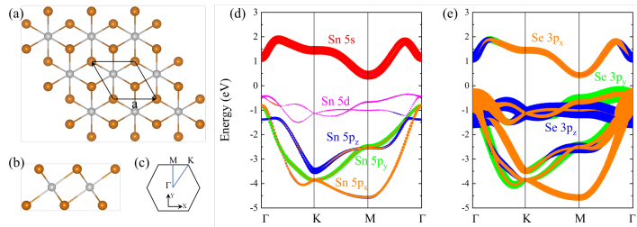
Unlike traditional TMDCs with space group, single layer SnSe2 crystallizes in a 1T-phase structure with point group, as presented in Figs. 1(a)-(b). It includes a threefold rotation symmetry axis and a vertical mirror plane . The optimized lattice parameter a is 3.869 Å, the bond length of Sn-Se is 2.751 Å, and the distance between two Se plane is 3.193 Å. They are in line with previous resultsHuang et al. (2016); Gonzalez and Oleynik (2016). The projected band structures of Sn and Se atoms in single layer SnSe2 are presented in Figs. 1(d)-(e). Single layer SnSe2 is an indirect-gap semiconductor; the conduction band minimum (CBM) is located at the M point, while the valence band maximum (VBM) is slightly away from the point (energy difference 85 meV). The PBE-calculated indirect band gap between the and M points is about 1.580 eV, consistent with a reported value of 1.690 eVGonzalez and Oleynik (2016). Our result shows that the presented six bands in low energy window mainly involve the and orbitals of Sn and Se atoms. The first and second valence bands at the point are doubly degenerate, with orbital decomposition of the corresponding wave function = 0.307 Se+0.952 Se. And the wave function of the CBM is = 0.789 Sn+ 0.535 Se + 0.179 Se +0.241 Se.
It is well known that DFT usually underestimates the band gap of semiconductors. We therefore have performed the GW calculation to get reliable quasi-particle band gap of monolayer SnSe2. Similar to those found in other monolayer 2D semiconductors, such as monolayer hexagonal TMDCsZhong et al. (2015) and phosphoreneTran et al. (2014), significant self-energy enhancements are observed in SnSe2; at the “single-shot” G0W0 level, the quasi-particle band gap at point of monolayer SnSe2 is increased to be 2.750 eV. Self-consistent GW (sc-GW) scheme beyond single-shot calculations has been verified to be necessary for some 2D semiconductors. Hence, we perform one self-consistent update to the Green’s function G; the quasiparticle band gap is further increased to be 3.069 eV. More self-consistent steps only slightly change the band gap ( 0.1eV) and we stop at the sc-G1W0 level. Finally, the enhanced many-electron effects enlarge the band gaps, but do not change the dispersion shape. The energy difference between the VBM and point is about 77 meV, which is nearly the same with the PBE-calculated value. In the following, all our discussions are based on the finalized sc-G1W0 results.
IV Tight-binding model
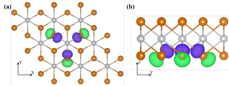
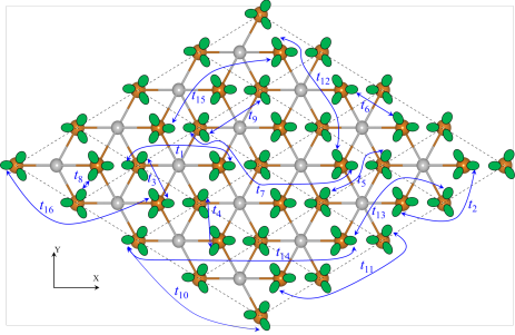
Given that the valence and conduction bands are dominated by and orbitals, and that they are separated from other states, it is possible to provide an accurate description of those states in terms of a tractable TB model in the low-energy region. Our parametrization procedure used in this work is based on the formalism of Maximally Localized Wannier Functions (MLWFs), and six orbitals are obtained as the basis for the TB model. A real-space distribution of the MLWFs obtained for single layer SnSe2 is shown in Fig. 2, where a combination of three orbitals localized on each Se atom, giving rise to six MLWFs per cell on two sublattices. The three orbitals are equivalent with a rotational symmetry of 2/3, effectively reducing the independent TB parameters.
The resulting non-relativistic TB model is given by a 6 by 6 effective Hamiltonian. The matrix elements of the Hamiltonian in Bloch-representation is
| (1) | ||||
Where tαβ is the effective hopping parameter describing the interaction between and orbitals residing at central and neighbour atoms, respectively. To make the model more tractable yet accurate enough, we first discard the hoppings with an interatomic distance larger than 11.620 Å, then ignore hopping parameters with amplitudes 19 meV. The residual hopping parameters are furthre re-optimized by minimizing the following least square function
| (2) |
where is the hopping in Eq. (1), () corresponds to the eigenvalues of G1W0 (TB) Hamiltonian with and being the band index and momenta along the high-symmetry in the first Brillouin zone, respectively. In order to get much more reliable results near the band edge, we add a Gaussian function here, in which is the energy of VBM/CBM from G1W0 approximation. The remaining orbitals and relevant hopping parameters are schematically shown in Fig. 3 and Table 1.
| 1 | -1.513 | 5.491 | 7 | -0.093 | 8.664 | 13 | 0.024 | 6.717 | ||
| 2 | -0.681 | 3.869 | 8 | -0.093 | 3.897 | 14 | -0.020 | 11.617 | ||
| 3 | 0.636 | 3.897 | 9 | -0.058 | 3.869 | 15 | 0.047 | 7.738 | ||
| 4 | 0.399 | 3.897 | 10 | -0.041 | 7.738 | 16 | -0.019 | 8.664 | ||
| 5 | 0.285 | 3.869 | 11 | 0.076 | 6.717 | |||||
| 6 | 0.300 | 3.869 | 12 | 0.056 | 6.701 |
Considering the inversion symmetry of atomic structure, our reciprocal space Hamiltonian matrix in Eq. (1) can be represented as
| (3) |
where and are 3 3 matrices describing the intra- and inter-sublattice interactions, respectively. The subscript in U() indicates rotation in the opposite direction, resulting from the vertical mirror symmetry . Because the three basic orbitals have threefold rotation symmetry , the corresponding matrices have the form
| (4) |
and
| (5) |
where and are the vector rotated by 2/3 and 4/3, respectively. The matrix elements in Eqs. (4)and (5) are
| (6) | ||||
| (7) | ||||
| (8) | ||||
| (9) | ||||
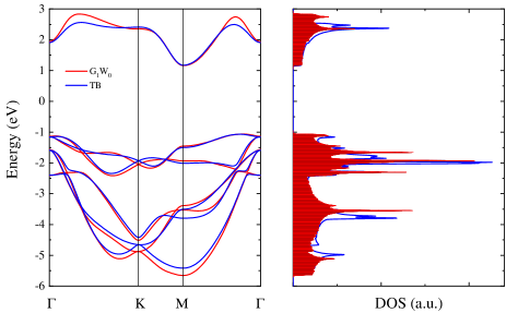
The band structure and density of states (DOS) obtained from the given TB model are shown in Fig. 4. The quasi-particle energy within G1W0 is plotted for comparison. One can see a good match between the TB and original first-principles calculations, especially for the band edges. This can be further quantified by the band gaps and effective masses analysis, which are accurately reproduced by the given TB model as shown in Table 2. The indirect (direct) band gaps obtained from TB model are 2.331 (3.066) eV, in good agreement with the value of 2.295 (3.070) eV in G1W0 calculation. This consistence is also remarkable in the effective masses of carriers in single-layer SnSe2. The anisotropic effective masses of electrons along the K-M and -M direction are 0.558 and 0.202 in the proposed TB model, and the corresponding values from G1W0 are 0.650 and 0.202 , respectively. Thus, our proposed TB model can be used effectively in describing the electronic, optical and transport properties of single layer SnSe2.
| Energy gap | Electrons | Holes | ||||
|---|---|---|---|---|---|---|
| Method | GM | GG | KM | GM | GK | GM |
| DFT+GW | 2.295 | 3.070 | 0.650 | 0.202 | 1.133 | 0.913 |
| TB | 2.331 | 3.066 | 0.558 | 0.202 | 1.261 | 0.854 |
V magneto-electronic properties
To go deeper, we investigate the electronic and optical properties of single-layer SnSe2 with external magnetic field, which is still a challenge in DFT calculation. In the case of a perpendicularly applied magnetic field , the hopping term between two sites in Eq. 1 is replaced by
| (10) |
where = hc/e is the flux quantum, and A = (-By, 0, 0) is the vector potential in the Landau gauge, respectively. The quantifying magnetic field leads to discrete DOS as the Landau Level (LL) peaks, which are presented in Fig. 5. The geometrical broadening in the LLs is owing to the energy resolution and total number of time steps in the tight-binding propagation method, which is limited by the calculated sample size (number of atoms). Because the electrons and holes are not symmetric in single layer SnSe2, the obtained LL spectrum consists of two sets of equidistant LLs, which can be simply described as
| (11) |
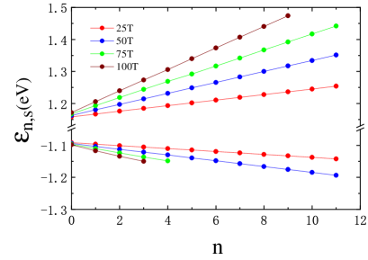
Where denotes the conduction and valence bands, is the energy at the conduction and valence band edge, is the Landau index, and = / is the relative ratio between free electron and the average effective masses at the band edges. For all investigated magnetic field, the LL spectrum follows well the linear dependence on in Eq. 11 with fitting values of = 1.154 (-1.090) eV and = 2.999 (1.382), respectively, as shown in Fig. 6. On the other hand, the LL spectrum also exhibits linear dependence with , which is similar to a typical 2D electron gas. Unlike the in massive Dirac system (sgn(n)), the landau index in Eq. 11 resembles to that of Schrdinger fermions ((n+)).
Then, we further study the optical magneto-conductivity of single layer SnSe2 using the Kubo formula
| (12) | ||||
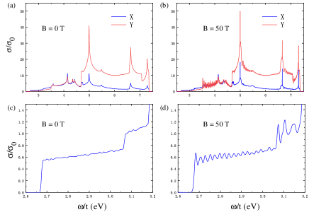
where , is the sample area, is the Fermi-Dirac distribution operator, is the chemical potential, and the time-dependent current operator in the (x or y) direction . Fig. 7 shows the optical conductivity spectrum of single layer SnSe2 along X and Y directions with and without magnetic field. The sample here is the same as in that the LLs calculation with 106 atoms. When no external magnetic field is applied (B = 0 T) in Fig. 7 (a), the optical spectrum shows obvious anisotropy, as a result of the anisotropic atomic structure. Specifically, the optical absorption along X direction is strong in the low energy region, but falls down to quarter of that along Y direction in the high energy region. A sharp increase appears at around 2.686 eV, corresponding to the direct optical transition from the highest valence band to the lowest conduction band at M point (2.634 eV). This correspondence confirms the reliability of our proposed TB model again. For the cases of B = 50 T in Figs. 7 (b) and (d), the continuous optical conductivity becomes quantized with discrete values, however, which are not very sharp as the cases for graphene and arseneYuan et al. (2010); Yu et al. (2018a). This is because that the highest valence band at M point is not discrete, clearly shown in the high energy part at -1.50 eV in the black window in Fig. 5(b). Thus, the magneto-optical spectrum can be classified into two categories, one is the direct-gap semiconductors like graphene with absolutely discrete peaks, and the other is indirect-gap semiconductors in this study with no sharp discrete values. Furthermore, the discrete peaks in single layer SnSe2 exhibit blue shifts with an increasing magnetic field. For example, when the magnetic field varies from 50 to 100 T, the first and second peak of the optical conductivity shifts from 2.684 and 2.707 eV to 2.693 and 2.744 eV, respectively.
VI Summary
In summary, we have proposed an effective Hamiltonian for single layer SnSe2 that is derived from six orbitals within the self-consistent GW approach. The model shows good performance with respect to the band structure and density of states comparable to those of the GW results, especially, in the low-energy region. Based on the derived TB model, the electronic and optical properties of single layer SnSe2 can be tuned effectively by a perpendicular magnetic field using the time-dependent propagation method. Because of the electron-hole asymmetry, the magnetic field yields two sets of Landau Level spectra. These spectra follow linear dependence on the field strength B and landau index n, confirming the nature of Schrdinger fermions. Additionally, single layer SnSe2 shows anisotropic optical responses due to its anisotropic atomic configurations. The starting point of the optical spectrum (2.686 eV) corresponds well with the quasi-energy gap at M point, validating the reliability of our proposed TB model. In the presence of external magnetic field, the optical conductivity presents some discrete peaks, but very different from those reported in direct-gap semiconductors. The TB model developed in our paper can be used for further exploring the electronic, optical, and transport properties of pristine and disordered SnSe2, especially in the presence of external magnetic fields.
Acknowledgements.
This work is supported by the National Key RD Program of China (Grant No. 2018FYA0305800). Hongxia Zhong acknowledges the support by China Postdoctoral Science Foundation (Grant No.2018M640723). Numerical calculations presented in this paper have been performed on a supercomputing system in the Supercomputing Center of Wuhan University.References
- Wang et al. (2012) Q. H. Wang, K. Kalantar-Zadeh, A. Kis, J. N. Coleman, and M. S. Strano, Nat. Nanotechnol. 7, 699 (2012).
- Jariwala et al. (2014) D. Jariwala, V. K. Sangwan, L. J. Lauhon, T. J. Marks, and M. C. Hersam, ACS Nano 8, 1102 (2014).
- Zhong et al. (2016) H. Zhong, R. Quhe, Y. Wang, Z. Ni, M. Ye, Z. Song, Y. Pan, J. Yang, L. Yang, M. Lei, et al., Sci. Rep. 6, 21786 (2016).
- Cercellier et al. (2007) H. Cercellier, C. Monney, F. Clerc, C. Battaglia, L. Despont, M. Garnier, H. Beck, P. Aebi, L. Patthey, H. Berger, et al., Phys. Rev. Lett. 99, 146403 (2007).
- Rohaizad et al. (2017) N. Rohaizad, C. C. Mayorga-Martinez, Z. Sofer, and M. Pumera, ACS Appl. Mater. Interfaces 9, 40697 (2017).
- Zhang et al. (2015) Y. Zhang, P. Zhu, L. Huang, J. Xie, S. Zhang, G. Cao, and X. Zhao, Adv. Funct. Mater. 25, 481 (2015).
- Zhou et al. (2016) X. Zhou, Q. Zhang, L. Gan, H. Li, and T. Zhai, Adv. Funct. Mater. 26, 4405 (2016).
- Zhou et al. (2018) X. Zhou, X. Hu, S. Zhou, H. Song, Q. Zhang, L. Pi, L. Li, H. Li, J. Lü, and T. Zhai, Adv. Mater. 30, 1703286 (2018).
- Ying et al. (2018) J. Ying, H. Paudyal, C. Heil, X.-J. Chen, V. V. Struzhkin, and E. R. Margine, Phys. Rev. Lett. 121, 027003 (2018).
- Su et al. (2014) G. Su, V. G. Hadjiev, P. E. Loya, J. Zhang, S. Lei, S. Maharjan, P. Dong, P. M. Ajayan, J. Lou, and H. Peng, Nano Lett. 15, 506 (2014).
- Burton et al. (2016) L. A. Burton, T. J. Whittles, D. Hesp, W. M. Linhart, J. M. Skelton, B. Hou, R. F. Webster, G. O’Dowd, C. Reece, D. Cherns, et al., J. Mater. Chem. A 4, 1312 (2016).
- Hu et al. (2017) Y. Hu, B. Luo, D. Ye, X. Zhu, M. Lyu, and L. Wang, Adv. Mater. 29, 1606132 (2017).
- Xu et al. (2017) P. Xu, T. Fu, J. Xin, Y. Liu, P. Ying, X. Zhao, H. Pan, and T. Zhu, Sci. Bull. 62, 1663 (2017).
- Chen et al. (2018) J. Chen, D. M. Hamann, D. Choi, N. Poudel, L. Shen, L. Shi, D. C. Johnson, and S. Cronin, Nano. Lett 18, 6876 (2018).
- Luo et al. (2018) Y. Luo, Y. Zheng, Z. Luo, S. Hao, C. Du, Q. Liang, Z. Li, K. A. Khor, K. Hippalgaonkar, J. Xu, et al., Adv. Energy Mater. 8, 1702167 (2018).
- Li et al. (2016) G. Li, G. Ding, and G. Gao, J. Phys.: Condens. Matter 29, 015001 (2016).
- Guo et al. (2016) C. Guo, Z. Tian, Y. Xiao, Q. Mi, and J. Xue, Appl. Phys. Lett. 109, 203104 (2016).
- Pei et al. (2016) T. Pei, L. Bao, G. Wang, R. Ma, H. Yang, J. Li, C. Gu, S. Pantelides, S. Du, and H.-j. Gao, Appl. Phys. Lett. 108, 053506 (2016).
- Na et al. (2019) J. Na, Y. Kim, J. H. Smet, M. Burghard, and K. Kern, ACS Appl. Mater. Interfaces (2019).
- Roy et al. (2016) T. Roy, M. Tosun, M. Hettick, G. H. Ahn, C. Hu, and A. Javey, Appl. Rev. Lett 108, 083111 (2016).
- Yan et al. (2017) X. Yan, C. Liu, C. Li, W. Bao, S. Ding, D. W. Zhang, and P. Zhou, Small 13, 1701478 (2017).
- Zeng et al. (2018) J. Zeng, E. Liu, Y. Fu, Z. Chen, C. Pan, C. Wang, M. Wang, Y. Wang, K. Xu, S. Cai, et al., Nano Lett. 18, 1410 (2018).
- Zhou et al. (2015) X. Zhou, L. Gan, W. Tian, Q. Zhang, S. Jin, H. Li, Y. Bando, D. Golberg, and T. Zhai, Adv. Mater. 27, 8035 (2015).
- Su et al. (2013) Y. Su, M. A. Ebrish, E. J. Olson, and S. J. Koester, Appl. Phys. Lett. 103, 263104 (2013).
- Gonzalez and Oleynik (2016) J. M. Gonzalez and I. I. Oleynik, Phys. Rev. B 94, 125443 (2016).
- Shafique et al. (2017) A. Shafique, A. Samad, and Y.-H. Shin, Phys. Chem. Chem. Phys. 19, 20677 (2017).
- Reich et al. (2002) S. Reich, J. Maultzsch, C. Thomsen, and P. Ordejon, Phys. Rev. B 66, 035412 (2002).
- Mazurenko et al. (2016) V. Mazurenko, A. Rudenko, S. Nikolaev, D. Medvedeva, A. Lichtenstein, and M. Katsnelson, Phys. Rev. B 94, 214411 (2016).
- Rudenko and Katsnelson (2014) A. N. Rudenko and M. I. Katsnelson, Phys. Rev. B 89, 201408 (2014).
- Rudenko et al. (2015) A. Rudenko, S. Yuan, and M. Katsnelson, Phys. Rev. B 92, 085419 (2015).
- Rudenko et al. (2017) A. Rudenko, M. Katsnelson, and R. Roldán, Phys. Rev. B 95, 081407 (2017).
- Yu et al. (2018a) J. Yu, M. I. Katsnelson, and S. Yuan, Phys. Rev. B 98, 115117 (2018a).
- Liu et al. (2013) G.-B. Liu, W.-Y. Shan, Y. Yao, W. Yao, and D. Xiao, Phys. Rev. B 88, 085433 (2013).
- Cappelluti et al. (2013) E. Cappelluti, R. Roldán, J. Silva-Guillén, P. Ordejón, and F. Guinea, Phys. Rev. B 88, 075409 (2013).
- Yu et al. (2018b) J. Yu, E. van Veen, M. I. Katsnelson, and S. Yuan, Phys. Rev. B 97, 245410 (2018b).
- Kresse and Furthmuller (1996) G. Kresse and J. Furthmuller, Comput. Mater. Sci. 6, 15 (1996).
- Kresse and Joubert (1999) G. Kresse and D. Joubert, Phys. Rev. B 59, 1758 (1999).
- Perdew et al. (1996) J. P. Perdew, K. Burke, and M. Ernzerhof, Phys. Rev. Lett. 77, 3865 (1996).
- Blöchl (1994) P. E. Blöchl, Phys. Rev. B 50, 17953 (1994).
- Monkhorst and Pack (1976) H. J. Monkhorst and J. D. Pack, Phys. Rev. B 13, 5188 (1976).
- Pack and Monkhorst (1977) J. D. Pack and H. J. Monkhorst, Phys. Rev. B 16, 1748 (1977).
- Rohlfing and Louie (2000) M. Rohlfing and S. G. Louie, Phys. Rev. B 62, 4927 (2000).
- Deslippe et al. (2012) J. Deslippe, G. Samsonidze, D. A. Strubbe, M. Jain, M. L. Cohen, and S. G. Louie, Comput. Phys. Commun. 183, 1269 (2012).
- Ismail-Beigi (2006) S. Ismail-Beigi, Phys. Rev. B 73, 233103 (2006).
- Rozzi et al. (2006) C. A. Rozzi, D. Varsano, A. Marini, E. K. Gross, and A. Rubio, Phys. Rev. B 73, 205119 (2006).
- Mostofi et al. (2008) A. A. Mostofi, J. R. Yates, Y.-S. Lee, I. Souza, D. Vanderbilt, and N. Marzari, Comput. Phys. Commun. 178, 685 (2008).
- Yuan et al. (2010) S. Yuan, H. De Raedt, and M. I. Katsnelson, Phys. Rev. B 82, 115448 (2010).
- Yuan et al. (2011) S. Yuan, R. Roldán, and M. I. Katsnelson, Phys. Rev. B 84, 125455 (2011).
- Yuan et al. (2012) S. Yuan, T. Wehling, A. Lichtenstein, and M. Katsnelson, Phys. Rev. Lett. 109, 156601 (2012).
- Huang et al. (2016) Y. Huang, D. Zhou, X. Chen, H. Liu, C. Wang, and S. Wang, Chem Phys Chem 17, 375 (2016).
- Zhong et al. (2015) H.-X. Zhong, S. Gao, J.-J. Shi, and L. Yang, Phys. Rev. B 92, 115438 (2015).
- Tran et al. (2014) V. Tran, R. Soklaski, Y. Liang, and L. Yang, Phys. Rev. B 89, 235319 (2014).