Topological Anderson Insulator in electric circuits
Abstract
Although topological Anderson insulator has been predicted in 2009, the lasting investigations of this disorder established nontrivial state results in only two experimental observations in cold atoms [Science, 362 ,929 (2018)] and in photonic crystals [Nature, 560, 461 (2018)] recently. In this paper, we study the topological Anderson transition in electric circuits. By arranging capacitor and inductor network, we construct a disordered Haldane model. Specially, the disorder is introduced by the grounding inductors with random inductance. Based on non-commutative geometry method and transport calculation, we confirm that the disorder in circuits can drive a transition from normal insulator to topological Anderson insulator. We also find the random inductance induced disorder possessing unique characters rather than Anderson disorder, therefore it leads to distinguishable features of topological Anderson transition in circuits. Different from other systems, the topological Anderson insulator in circuits can be detected by measuring the corresponding quantized transmission coefficient and edge state wavefunction due to mature microelectronic technology.
I introduction
Topological stateTIkane ; zhang ; xue ; weyl1 ; weyl2 ; HOTI is one of the most fascinating research areas in the past decades for its exotic properties. Due to the urgent need of applications in low-dissipative devices, the disorder effect in topological states has also been widely investigatedLi ; Hua1 ; Chen1 ; Chen2 ; Chen3 ; song1 ; song2 ; WYJ ; Flo1 ; Flo2 ; hug1 ; hug2 ; Nagaosa1 ; Nagaosa2 ; HOdis with the emergence of a variety of materials. Most studies indicate topological states are robust against weak disorder Chen2 ; hug1 ; HOdis and their nontrivial features disappear under strong disorder. Surprisingly, disorder does not always destroy topological propertiesLi ; Hua1 ; Chen1 ; WYJ ; Flo2 ; hug1 . In , by studying the effect of Anderson disorder in HgTe/CdTe Quantum wells BHZ1 ; BHZ2 ; Hua1 ; Li , an interesting transition where a normal insulator becomes a topological insulator were predicted. This means disorder can also establish a topological state, which was named as topological Anderson insulator (TAI) Li . Later, TAI was explained by self-consistent Born approximation method, where disorder renormalizes the Hamiltonian with changing band structure from normal to inverted lilun . The TAI and related topological transition have generated intensive studies in the last ten yearsChen1 ; Chen3 ; song1 ; Flo1 ; Flo2 ; HMGUO ; reveiwDisorder ; 2011 ; 2013 ; 2014 . However, until more recently, TAI phase was experimentally confirmed by two independent groups. They find the existence of TAI transition in cold atom shiyan1 and photonic crystal systems shiyan2 , respectively.
Recently, topological states simulated in the electric circuits also attract great attentions in condensed matter physics LCrev1 ; LCrev2 ; u1h1 ; u1h2 ; LCwey1 ; LCwey2 ; LCTB ; LCHO1 ; LCHO2 ; LCorbit ; LCgreen ; LCchern1 ; LCchern2 ; LCedge ; LCkane . The realization of hopping phase u1h1 ; u1h2 suggests the possibility of simulating the effect of magnetic field and the appearance of Hofstadter Butterfly Hofsta in circuits. Various topological states have also been implemented, such as quantum spin Hall statesu1h1 , Weyl semimetalsweyl1 ; weyl2 , higher order topological insulator LCHO1 and quantum anomalous Hall statesLCchern1 ; LCchern2 . Compared with cold atoms and photonic crystals, parameters in circuits is easier to be controlled and physical quantities are more convenient to be measuredLCrev1 ; LCrev2 ; LCHO1 ; LCgreen . Since wave function in circuits is the voltage of each nodesLCrev1 ; LCrev2 and Green’s function corresponds to the impedance, both the wave function and the Green’s function can be directly observedLCHO1 . For example, based on the impedance and voltage measurement, the detection of band spectrumLCgreen , curvatures LCwey2 , zero energy stateLCHO1 ; LCHO2 and even orbital angular momentumorbit ; LCorbit have been realized. These results manifest promising potential of circuits simulations in topological states.
In this paper, we propose a feasible method to realize TAI in circuits. By using cross connection method we rebuilt the Haldane model with disorder in electronic system. The topological nature of Haldane model can be controlled by selected inductors and the disorder is introduced by random inductance induced on-site potential . Then, the possibility of TAI in our model is checked with the help of Chern number and transmission coefficient calculation. We find TAI exists in circuits. Furthermore, we also find topological Anderson transition in circuits is not the same to condensed matter conditions. The feature comes from the special distribution of rather than that of Anderson disorder. Compare with cold atoms and photonic crystals, the wave function and the Green’s function in circuits correspond to the voltageLCrev1 and the impedanceLCHO1 , which are both easier to be measured. Therefore, we propose the detection of the wave function (edge states) and Chern numberThouless (quantized transmission coefficient ) as the smoking gun evidences for TAI in circuits. In addition, because of essential topological properties, one can determine TAI in circuits with need of only one dirty sample.
The rest of this paper is organized as follows: In Sec., we show the construction of disordered Haldane model in electric circuits. In Sec., we obtain the general condition of realization of TAI in circuit. In Sec., we study the difference of TAI behavior between random inductance induced disorder and Anderson disorder. In Sec., we present experimental detection of TAI in circuits. Finally, a brief discussion and summary are presented in Sec..
II Theoretic model
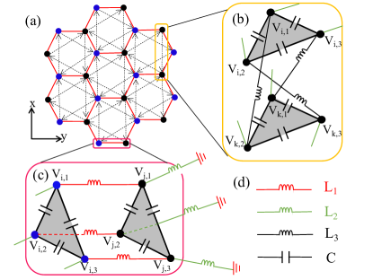
We begin with construct a Haldane model with the help of circuits. Haldane model is made of honeycomb lattice [see Fig. 1(a)], where nearest and next nearest hopping exist between A/B sublattice sites. As illustrated in Fig. 1(b) and (c), we firstly construct a triangle in gray color with three connected capacitors with the same capacitance and the voltages of all nodes are marked by . Every triangle could be considered as a site in honeycomb lattice and the color of triangle nodes represent the corresponding sublattice. Next, three kind of inductances are used to simulate the nearest, next nearest hopping and on-site energy [see Fig. 1 (b)-(d)]. The red and black inductors stand for the nearest hopping and next-nearest hopping. Each node is also grounded by green inductor . Fig. 1(c) shows the realization of the nearest hopping in circuits where of the left triangle is directly connected to of the right triangle. The next nearest hopping shown in Fig. 1(a) is realized in a different way. We let cross connected with , i.e. is connected with , as shown in Fig. 1(b). This cross connection method can induce a hopping with geometry phase, and has been used in previous studies to realize quantum spin Hall in circuits u1h1 ; u1h2 .
Following, we briefly introduce the relationship of Haldane model and the above circuit network. Based on Kirchhoff’s lawLCHO1 ; LCrev1 , the AC current and the node voltage in a circuit satisfy:
| (1) | ||||
where is the current of node , is the voltage at node , is the inductance between nodes and , is the inductance between nodes and the ground, is the capacitance between nodes and . The summation are taken over all nodes and which are connected with by inductors and capacitors, respectively.
In our model, the voltage and current for site can be written in vector form . By applying Eq.(1) and , one obtain
| (2) | ||||
where
| (3) |
and identity matrix . The summation are taken over all the nearest and next nearest sites. Because of cross connection between site and [see Fig. 1(b)], . Then, Eq.(2) can be written as
| (4) | ||||
where and indicate three nearest and six next nearest neighbors LCkane , and
| (5) |
If there is no input current in circuit, . By defining , Eq.(4) has the following form:
| (6) | ||||
If one analogizes with wavefunction, the above equation is close to the eigenequation for Haldane model with () the nearest (next nearest) hopping. The major difference comes from that is not diagonalized. In order to simulate Haldane model physics, we then perform unitary transformation with matrixu1h1 ; u1h2 :

| (7) |
Because , can simultaneously diagonalize and into and . The unitary matrix is not changed under such transformation. Therefore, Eq.(6) can be rewritten in new bases :
| (8) | ||||
where . From above equation, is independent of , which is reasonable to be discarded in the following . Thus, Eq.(8) can be divided into two independent equations,
| (9) | ||||
| (10) | ||||
Eqs. (9) and (10) are nothing but the eigenequation for Haldane model. If we regard , as spin and wavefunction, the whole system resembles quantum spin Hall phaseHaldane ; kanemele , where the corresponding spin component is decoupled Haldane model. Since two spin components are related by time reversal symmetryLCrev1 ; u1h1 ; u1h2 ; LCkane , the topological properties of the system can be characterized by one of the spin (i.e. or ).
In the following, we only focus on the Haldane model with spin (). From Eq. (9), the Haldane model has geometry phase . The energy , nearest hopping and next nearest hopping can be determined by corresponding inductances and capacitances. More importantly, the on-site energy has an independent parameter . If one introduces the randomization to , the on-site disorder can be achieved. This may pave a way on realization and detection of exotic TAI in electric circuits. We note the Haldane model without and with other geometry phase was achieved in circuit experiment previouslyu1h1 . The geometry phase breaks the particle-hole symmetry, which is benefitial to the topological Anderson transition.
III TAI in Haldane model
In above section, we have demonstrated the construction of a special Haldane model in circuit. In this section, we study the general condition for realization of TAI in such Haldane model by considering the major characteristic of circuit (i.e. geometry phase as well as positive inductance and capacitance value etc).
Eq.(9) is equivalent to tight-binding HamiltonianHaldane :
| (11) | ||||
where are the annihilation operators of A and B sublattices. The first and second terms are nearest and next nearest hopping with and , respectively. For convenience, the hopping energy is fixed at , in the rest of this paper. The second line represents the on-site potential terms by . We ignore , , because they only adjust the Fermi level and the topological nature is not affected. In order to obtain a disorder induced topological Anderson transition, the system should be a normal insulator in the clean limit. However, without stagger potential, the studied model is always topological insulator. Fortunately, one can independently adjust for each site. Thus, not only a stagger potential for A/B sublattice, but also the Anderson disorder for each site can be introduced. Therefore, the on-site energy terms are separated into four sub-terms. , with indicates the on-site potential for A, B sublattice. is Anderson disorderanderson which is uniformly distributed in the range with the disorder strength . In real experiments, one can contact each sites with two grounding inductors in parallel to simulate the effect of for simplicity. That is to say, one inductor with value simulates the stagger potential, another inductor of random inductance simulates the disorder . The total on-site energy . We note can capture the major function of Anderson disorder, the general results in this section will not change even by considering their difference. We will discuss the similarity and the difference in Sec..
The band structures for zigzag nano-ribbon with different are plotted in Fig. 2 [here, we call versus plots the band structure for simplicity]. When , on-site potential of A and B sublattice are equal and the system is a topological insulator. As shown in Fig. 2(a), the edge states appear in the bulk gap, while is not considered for simplicity. In order to observe the topological Anderson transition, trivial states should be prepared firstly. Theoretically, it is impossible to realize negative on-site energy in circuits. That is to say, a real stagger potential for A/B sublattice that was pointed out by Haldane Haldane can not be achieved in our system. However, if is larger than the topological gap, a trivial state can also appear. Therefore, a normal insulator is available even when and . A transition from topological insulator to normal insulator happens when is increased to , as plotted in Fig. 2 (b).
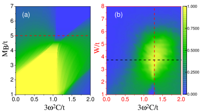
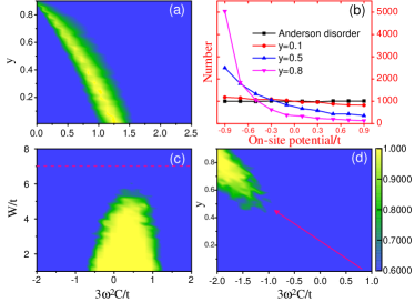
In order to make above topological transition more convincingly, the dependence of the Chern number on the energy for different is demonstrated in Fig. 3(a) with the help of non-commutative geometry methodsong2 ; hug1 ; hug2 ; FDY1 ; FDY2 ; FDY3 . For , Chern number is quantized when , which is consistent with the spectrum shown in Fig. 2(a). Once , bulk states become metallic and Chern number is no longer quantized. Moreover, the area of topological states is decreased with the increase of and topological phase totally disappears when . In particular, the calculation reconfirms that [marked by red dashed line in Fig. 3(a))] is a normal insulator. Such normal insulator is the starting point to pursue TAI in circuit.
Since non-commutative geometry method is based on real space wave function, we are able to obtain the evolution of Chern number of the Haldane model with the variation of disorder strength . If Chern number becomes quantized under a fixed when , it enters into the TAI. As shown in Fig. 3(b), Chern number is almost quantized when , for a square sample. We also find the quantized Chern number area is growing by increasing sample size due to the finite size effectFinSize . Guiding by Fig. 3(b), we propose the red dotted line case () as the best condition to realize TAI in circuits.
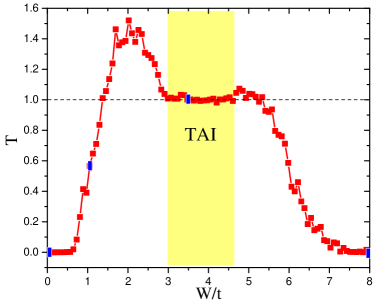
The transport simulation is also widely used to better characterize the TAI phase. It is known that the quantized transmission coefficient is equal to the number of edge states and the Chern number even for dirty samples. The transmission coefficient versus disorder is obtained from nonequilibrium Green function method datta ; Hua1 and is plotted in Fig. 4. For clean samples, the transmission coefficient is zero, which indicates its insulating properties. Then, the band structure is renormalizedChen1 ; song1 ; lilun with the increase of disorder strength . If is large enough, bulk gap closes and the transmission coefficient is finite, but not quantized. However, for , transmission coefficient becomes quantized, which clearly manifests the disorder induced topological Anderson transition (filled with yellow in Fig. 4). If one continues to increase , all states are localized with decreasing of transmission coefficient finally. These results are well consistent with Fig. 3(b).
IV Comprehensive understanding of disorder in circuit
In section III, based on Anderson disorder simulation in Haldane model, we verify that TAI phase can in principle exist in electric circuit. However, the disorder (randomness of inductor) in circuit may posses its own characteristic, making its consequence more or less different from Anderson disorder. In this section, we present a comprehensive study.
Anderson disorder is uniformly distributed in the range with disorder strength . Because negative on-site potential is not accessible in circuits, we will design some alternative scheme to achieve the function of Anderson disorder in such system. We also compare the scheme with standard Anderson disorder. Suppose node is grounded by a inductor with value , on-site potential will be added by . If different nodes are grounded by the inductor with different inductance , disorder can be realized. The first scheme is to choose inductor with value between and to let the on-site potential in the range . The case discussed above is equivalent to that A/B sublattice potential is changed to and disorder is still in the range . Since initial topological index of the system is still determined by stagger potential , this scheme only shifts Fermi energy but not changes the topological Anderson transition. The scheme can simulate Anderson disorder well. However, the value of inductors should be carefully picked to achieve a uniform distribution of on-site potential and inductors with huge value will be needed. Although this scheme is feasible in principle, it is hard for experimental implementation.
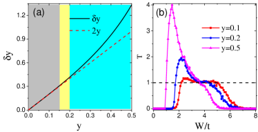
Another scheme is to make use of the error ratio of inductors with inductance . We hope randomness of inductor could induce a disorder that like Anderson type disorder. Let the accurate inductance . Due to the fluctuation, the realistic inductance is in between LCHO1 . Thus, the difference between the maximum and minimum on-site potential induced by error ratio is . The Fermi energy of is shifted up to , which has no influence on topological properties. To compare random inductance induced disorder with Anderson disorder, we plot the evolution of with the increase of in Fig. 5(a). The red dashed line represents the standard Anderson disorder with uniform distribution and the difference between the maximum and minimum value is . The black line represents the random inductance induced disorder with . Because the black line and the red dashed line are completely coincident when , the random inductance induced disorder can simulate Anderson disorder quite well. Random inductance induced disorder deviates from Anderson disorder when . When , and show sharp difference behavior . Therefore, random inductance induced disorder and Anderson disorder have totally different distributions.
In order to find the differences among these three inductance error ratio regions marked in Fig. 5(a), we also study the influence of with the same disorder strength . Firstly, we generate an inductance with its error unit distribution in the range . The on site potential cause by is
| (12) |
Here, is the shift of Fermi energy, which should be substracted. From above paragraph, the on-site potential difference defines the disorder strength as . Then, by substituting with in Eq. (12), one obtain the on-site potential induced by
| (13) |
From Eq. (13), we not only obtain the on-site potential caused by inductance error in circuit Haldane model, but also can compare the effect of different with the same .
The evolution of transmission coefficient for different value of (, , ) is plotted in Fig. 5(b). For , the inaccurate inductance induced disorder can simulate Anderson disorder well. The transmission coefficient is quantized when , which is almost the same as the results in Fig. 4. Such result once again verifies that TAI phase can be obtained in the frame of circuit system. For , deviates from Anderson type disorder. Although the transmission coefficient plateau still exists, the plateau width shrinks greatly. However, is totally different from Anderson disorder for [see Fig. 5(a)]. The plateau disappears, which means the TAI is not available.
Now, we fix disorder strength to study how error ratio affects topological Anderson phase [see Fig. 6(a)]. The topological region is gradually deflected toward the low energy direction with the increase of . Remarkably, we also find, by increasing , the energy window for TAI is gradually decreased. And it disappears when approaches . In order to understand above phenomenon, we calculate the distribution of , as shown in Fig. 6(b). For the fixed disorder strength , we randomly generate 10000 numbers of between and by Eq.(13) and divide them into equal intervals [i.e. ]. Then the frequency that appears in each interval range is counted, as shown in Fig. 6(b). The statistics of Anderson disorder, which is uniformly distributed, is also plotted for comparison. For , random inductance induced disorder almost agrees with Anderson disorder, which is consistent with the previous analysis. With the increase of , the curves gradually deviates from Anderson disorder. Interestingly, the counting number is greatly increased for small . Since is not symmetric about the origin, the topological region deflects toward the low energy direction for TAI [see Fig. 6(a)]. Moreover, as shown in Fig. 6(b), the on-site potential is mainly concentrated in a small range for [e.g. ]. In this case, plays a role as weak disorder rather than strong disorder. It can greatly shift the Fermi energy but has little effect on the renormalization of topological mass from positive to negative lilun . Consequently, the sample tends to become clean, and thus topological Anderson phase is gone.
To confirm such speculation, we also study the influence of on the transition from Chern insulator to Anderson insulator caused by strong disorder. In Fig. 6(c), the evolution of Chern number under Anderson disorder is plotted. We set and the clean system belongs to topological insulator. For [see red line in Fig. 6(c)], the Anderson disorder drives the system into the Anderson insulator phase and a zero Chern number is obtained. Then, we fix disorder strength but replace the Anderson disorder with the random inductance induced disorder . Fig. 6(d) plots evolution of Chern number under different . Topological states reappear with large . This shows strong evidence that, even for fixed disorder strength , the disorder effect of becomes weaker and weaker by increasing . Finally, the sample is close to the clean sample in large limit.
Conclusively, the random inductance induced disorder in circuit plays the same role as Anderson disorder when error ratio is small. However, the random inductance induced disorder and Anderson disorder show different behaviors when is larger. Ultimately, the disordered circuit with large enough behaves like a clean system, where the topological Anderson transition cannot be achieved.
V Experimental detection of TAI in circuits
Thus far, based on Haldane model in electric circuits, we have confirmed the existence of TAI. The well developed electrical techniques not only make the construct of TAI in circuit feasible, but also provide a simple way to detect such phase. In the following, we demonstrate two methods to detect TAI phase on account of circuit characteristics.
The first method is based on Green’s function. Different from condensed matter system, Green’s function is the impedanceLCHO1 in circuits, which can be directly measured. From Kirchhoff’s current law, we obtain
| (14) |
with and is the Hamiltonian. If there is an input current at node , the voltage of node satisfies and Green’s function can be obtainedLCgreen . Therefore, for a square sample with sites, the entire Green’s function can be detected through times input of node current. Then, the Hamiltonian is and all the information of dirty sample can be achieved. Interestingly, the detection of transmission coefficient is much easier in experiment. According to previous theorydatta ; PNjunction , only the Green’s function between the and the principle line
| (15) |
is need. Here, the left/right semi-infinite lead [source and drain] information is not measured. However, since there is no disorder, the retarded self-energy of these two leads can be numericallyzineng1 ; zineng2 obtained. Then, one gets retarded Green’s function of sample according to Dyson’s equationDyson . Finally, with the help of non-equilibrium Green’s function methoddatta , the transmission coefficient is expressed as with . As shown in Fig. 4, transmission coefficient should be quantized () once there is a topological Anderson transition. Nevertheless, Fig. 4 is difficult to be obtained experimentally since it is hard to frequently change disorder strength in circuit. Fortunately, the feature of TAI can be confirmed from transmission coefficient with twice measurements. Because, one can easily measure the evolution of for different energy in a clean sample () and the transmission coefficient for a sample with fixed disorder strength . will be quantized to one (zero) in a scope of for TAI (normal insulator), as shown in black line in Fig. 3(b) [red line in Fig. 3(a)].
We emphasize in Eq. (14), the effective current is not a direct input quantity. In our circuit model, the real input current for site should satisfy . If meets the following relations
| (16) |
one obtain . This means only spin up modes of Haldane model (Eq.(9)) are excited. And from Eq.(14), one can obtain the Green’s function and Hamiltonian for spin up Haldane model.
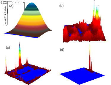
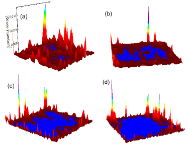
Another feasible method is to measure the spatial distribution of wave function. As stated in Sec. II, voltages in circuits correspond to wave functions in condensed matter physics. Experimentally, voltage is much easier to be measured by voltmeter and it has been widely used in topological state studies of circuit LCrev2 ; u1h1 . Therefore, if an inductor is excited, the propagation of the excitation makes wave function measurableLCedge . Thus, the detection of edge states under different disorder can be used to verify the existence of TAI. The evolution of wave function under disorder strength , , , (marked in Fig. 4 by rectangles) is plotted in Fig. 7. Since it is a normal insulator for clean sample, the wave function is mainly located on the center of the sample [see Fig. 7 (a)]. With increasing , the eigen-state spreads to the whole sample and belongs to metallic state for . When , the wave function distributes mainly on the edge, which indicates the topological nature of TAI. In the end, all states are totally localized for and the transmission coefficient is zero because of Anderson localization. In order to make the signal of TAI more clear, the examination of the wave function on the sample size is also suggested. Fig. 8 shows distribution of wave function under different size at . When is too small, e.g. , the edge states belong to opposite edges will couple with each other due to finite size effect, making the TAI undetectable. However, for large , the distribution of edge state becomes obvious and insensitive to . So, it is very easy to be detected when . The size simulation not only provides a way to find the appropriate experimental condition for TAI, but also reveals the topological nature of TAI.
Specially, different from cold atom systems and photonic crystal systems, where either edge states or quantizied transmission coefficient is difficult to be observed, one can detect these two quantities simultaneously in circuit.
VI Discussion and Conclusion
Finally, we propose the appropriate parameters and system sizes for realizing TAI in detail. Take as the unit. The nearest and next nearest hopping can be realized with inductance set as and . Furthermore, the value of accurate grounding inductors, which stimulate the stagger potential for A/B sublattice, are and , respectively. In addition, Anderson disorder with strength can be achieved by inductance with error ratio and the Fermi energy shift is approximately . Therefore, the best Fermi energy by adding omit shift is , with denotes input frequency and denotes capacitance. Experimentally, if we set , and , the other parameters are as follows. The accurate grounding inductors for A/B sublattice are and , respectively. The disordered grounding inductors have the value and input frequency for current or voltage is with system size .
In summary, we present a scheme for implementing TAI in electric circuits by constructing disordered Haldane model. With the help of Chern number calculation, we demonstrate that TAI can be realized through random inductance induced disorder . However, the topological Anderson transition in circuit poses its own properites. For small inductance error ratio , and Anderson disorder have similar distribution, the topological Anderson phase can be obtained. For larger , the two kinds of disorder show a sharp contrast in distribution, the topological Anderson phase will be not available. Finally, based on the measurement of wave function and transmission coefficient in circuit, two experiments are suggested to detect TAI. Specially, due to the nontrivial property, TAI can be fabricated and be measured even with only one dirty circuit sample.
VII ACKNOWLEDGMENTS
We are grateful to R. Yu, C. Z. Chen and Q. J. Wang for helpful discussion. This work was supported by NSFC under Grant Nos. 11534001, 11822407, 11874139, NSF of Jiangsu Province under Grants Nos. BK2016007 and a Project Funded by the Priority Academic Program Development of Jiangsu Higher Education Institutions (PAPD).
References
- (1) M. Z. Hasan and C. L. Kane, Colloquium: topological insulators, Rev. Mod. Phys. 82, 3045 (2010).
- (2) X.-L. Qi and S. C. Zhang, Topological insulators and superconductors, Rev. Mod. Phys. 83, 1057 (2011).
- (3) C. Z. Chang, et al. , Experimental observation of the quantum anomalous Hall effect in a magnetic topological insulator, Science 340, 167 (2013).
- (4) B. Q. Lv, et al., Experimental discovery of Weyl semimetal TaAs, Phys. Rev. X 5, 031013 (2015).
- (5) S. Y. Xu, et al., Discovery of a Weyl fermion semimetal and topological Fermi arcs, Science 349, 613 (2015).
- (6) F. Schindler, et al., Higher-order topological insulators, Sci. Adv. 4, eaat0346 (2018).
- (7) J. Li, R. L. Chu, J. K. Jain and S. Q. Shen, Topological anderson insulator, Phys. Rev. Lett. 102, 136806 (2009).
- (8) H. Jiang, L. Wang, Q. F. Sun and X. C. Xie, Numerical study of the topological Anderson insulator in HgTe/CdTe quantum wells, Phys. Rev. B 80, 165316 (2009).
- (9) C. Z. Chen, J. T. Song, H. Jiang, Q. F. Sun, Z. Q. Wang and X. C. Xie, Disorder and metal-insulator transitions in Weyl semimetals, Phys. Rev. Lett. 115, 246603 (2015).
- (10) C. Z. Chen, H. W. Liu, H. Jiang and X. C. Xie, Positive magnetoconductivity of Weyl semimetals in the ultraquantum limit, Phys. Rev. B 93, 165420 (2016).
- (11) C. Z. Chen, H. W. Liu, X. C. Xie, Effects of Random Domains on the Zero Hall Plateau in the Quantum Anomalous Hall Effect, Phys. Rev. Lett. 122, 026601 (2019).
- (12) J. T. Song, H. W. Liu, H. Jiang, Q. F. Sun and X. C. Xie, Dependence of topological Anderson insulator on the type of disorder, Phys. Rev. B 85, 195125 (2012).
- (13) J. T. Song, E. Prodan, AIII and BDI topological systems at strong disorder, Phys. Rev. B 89, 224203 (2014).
- (14) Y. J. Wu, H. W. Liu, H. Jiang and X. C. Xie, Global phase diagram of disordered type-II Weyl semimetals, Phys. Rev. B 96, 024201 (2017).
- (15) R. Chen, D. H. Xu and B. Zhou, Floquet topological insulator phase in a Weyl semimetal thin film with disorder, Phys. Rev. B 98, 235159 (2018).
- (16) P. Titum, N. H. Lindner, M. C. Rechtsman and G. Refael, Disorder-induced Floquet topological insulators, Phys. Rev. Lett. 114, 056801 (2015).
- (17) E. Prodan, T. L. Hughes and B. A. Bernevig, Entanglement spectrum of a disordered topological chern insulator, Phys. Rev. Lett. 105, 115501 (2010).
- (18) I. Mondragon-Shem, T. L. Hughes, J. T. Song and E. Prodan, Topological criticality in the chiral-symmetric AIII class at strong disorder, Phys. Rev. Lett. 113, 046802 (2014).
- (19) K. Nomura and N. Nagaosa, Surface-quantized anomalous Hall current and the magnetoelectric effect in magnetically disordered topological insulators, Phys. Rev. Lett. 106, 166802 (2011).
- (20) M. Onoda, Y. Avishai and N. Nagaosa, Localization in a quantum spin Hall system, Phys. Rev. Lett. 98, 076802 (2007).
- (21) H. Araki, T. Mizoguchi and Y. Hatsugai, Phase diagram of a disordered higher-order topological insulator: A machine learning study, Phys. Rev. B 99, 085406 (2019).
- (22) B. A. Bernevig, T. L. Hughes and S. C. Zhang, Quantum spin Hall effect and topological phase transition in HgTe quantum wells, Science 314, 1757 (2006).
- (23) M. König, S. Wiedmann, C. Brüne, et al. Quantum spin Hall insulator state in HgTe quantum wells, Science 318, 766 (2007).
- (24) C. W. Groth, M. Wimmer, A. R. Akhmerov and C. W. J. Beenakker, Theory of the topological Anderson insulator, Phys. Rev. Lett. 103, 196805 (2009).
- (25) H. M. Guo, G. Rosenberg, G. Refael and M. Franz, Topological Anderson Insulator in Three Dimensions, Phys. Rev. Lett. 105, 216601 (2010).
- (26) B. L. Wu, J. T. Song, J. J. Zhou and H. Jiang, Disorder effects in topological states: Brief review of the recent developments, Chin. Phys. B 25 117311 (2016).
- (27) Y. X. Xing, L. Zhang and J. Wang, Topological Anderson insulator phenomena, Phys. Rev. B 84, 035110(2011).
- (28) Y. Y. Zhang and S. Q. Shen, Algebraic and geometric mean density of states in topological Anderson insulators, Phys. Rev. B 88, 195145 (2013).
- (29) Y. Su, Y. Avishai, X. R. Wang, Topological Anderson insulators in systems without time-reversal symmetry, Phys. Rev. B 93, 214206 (2016).
- (30) E. J. Meier, F. A. An, A. Dauphin, et al., Observation of the topological Anderson insulator in disordered atomic wires, Science, 362, 929 (2018).
- (31) S. Stützer, Y. Plotnik, Y. Lumer, et al., Photonic topological Anderson insulators, Nature, 560, 461 (2018).
- (32) E. Zhao, Topological circuits of inductors and capacitors, Ann. Phys. 399, 289 (2018).
- (33) C. H. Lee, S. Imhof, C. Berger, F. Bayer, J. Brehm, L. W. Molenkamp, T. Kiessling and R. Thomale, Topolectrical circuits, Comm. Phys. 1, 39 (2018).
- (34) N. Y. Jia, C. Owens, A. Sommer, D. Schuster and J. Simon, Time-and site-resolved dynamics in a topological circuit, Phys. Rev. X 5, 021031 (2015).
- (35) V. V. Albert, L. I. Glazman and L. Jiang, Topological properties of linear circuit lattices, Phys. Rev. Lett. 114, 173902 (2015).
- (36) K. Luo, R. Yu, H. Weng, Topological nodal states in circuit lattice, Research 2018, 6793752 (2018).
- (37) Y. Lu, N. Jia, L. Su, C. Owens, G. Juzelinas, D. I. Schuster and J. Simon, Probing the Berry curvature and Fermi arcs of a Weyl circuit, Phys. Rev. B 99 020302 (2019).
- (38) Y. Nakata, T. Okada, T. Nakanishi, and M. Kitano, Circuit model for hybridization modes in metamaterials and its analogy to the quantum tight binding model, Phys. Status Solidi B 249, 2293 (2012).
- (39) M. Ezawa, Higher-order topological electric circuits and topological corner resonance on the breathing kagome and pyrochlore lattices, Phys. Rev. B 98, 201402 (2018).
- (40) S. Imhof, C. Berger, F. Bayer, et al., Topolectrical-circuit realization of topological corner modes, Nat. Phys. 14, 925 (2018).
- (41) Y. Li, Y. Sun, W. Zhu, Z. Guo, J. Jiang, T. Kariyado, H. Chen and X. Hu, Topological LC-circuits based on microstrips and observation of electromagnetic modes with orbital angular momentum, Nat. Comm. 9, 4598 (2018).
- (42) T. Helbig, T. Hofmann, C. H. Lee, R. Thomale, S. Imhof, L. W. Molenkamp and T. Kiessling, Band structure engineering and reconstruction in electric circuit networks, Phys. Rev. B 99, 161114 (2019).
- (43) R. Haenel, T. Branch and M. Franz, Chern insulators for electromagnetic waves in RLC networks, arXiv:1812.09862, (2018).
- (44) T. Hofmann, T. Helbig, C. H. Lee, M. Greiter and R. Thomale, Chiral voltage propagation in a self-calibrated topolectrical Chern circuit, arXiv:1809.08687, (2018).
- (45) M. Serra-Garcia, R. Süsstrunk and S. D. Huber, Observation of quadrupole transitions and edge mode topology in an LC circuit network, Phys. Rev. B 99, 020304 (2019).
- (46) W. Zhu, Y. Long, H. Chen, and J. Ren, Quantum valley Hall effects and spin-valley locking in topological Kane-Mele circuit networks, Phys. Rev. B 99, 115410 (2019).
- (47) D. R. Hofstadter, Energy levels and wave functions of Bloch electrons in rational and irrational magnetic fields, Phys. Rev. B 14, 2239 (1976).
- (48) L. H. Wu and X. Hu, Scheme for achieving a topological photonic crystal by using dielectric material, Phys. Rev. Lett. 114, 223901 (2015).
- (49) D. J. Thouless, M. Kohmoto, M. P. Nightingale and M. den Nijs, Quantized Hall conductance in a two-dimensional periodic potential, Phys. Rev. Lett. 49, 405 (1982).
- (50) F. D. M. Haldane, Model for a quantum Hall effect without Landau levels: Condensed-matter realization of the parity anomaly, Phys. Rev. Lett. 61, 2015 (1988).
- (51) C. L. Kane and E. J. Mele, Quantum spin Hall effect in graphene, Phys. Rev. Lett. 95, 226801 (2005).
- (52) F. Evers and A. D. Mirlin, Anderson transitions, Rev. Mod. Phys. 80, 1355 (2008).
- (53) T. A. Loring and M. B. Hastings, Disordered topological insulators via algebras, Euro. Phys. Lett. 92, 67004 (2011).
- (54) E. Prodan, Disordered topological insulators: a non commutative geometry perspective, J. Phys. A-Math. Theor. 44, 113001 (2011).
- (55) M. B. Hastings and T. A. Loring, Topological insulators and algebras: Theory and numerical practice, Ann. Phys. 326, 1699 (2011).
- (56) B. Zhou, H. Z. Lu, R. L. Chu, S. Q. Shen and Q. Niu, Finite size effects on helical edge states in a quantum spin-Hall system, Phys. Rev. Lett. 101, 246807 (2008).
- (57) Electronic Transport in Mesoscopic Systems, edited by S. Datta(Cambridge University Press, Cambridge, UK, 1995).
- (58) L. Wen, Q.F. Sun and J. Wang. Disorder-induced enhancement of transport through graphene pn junctions. Phys. Rev. Lett. 101, 166806 (2008).
- (59) D. H. Lee and J. D. Joannopoulos, Simple scheme for surface-band calculations. I, Phys. Rev. B 23, 4988 (1981); D. H. Lee and J. D. Joannopoulos, Simple scheme for surface-band calculations. II. The Green’s function, Phys. Rev. B 23, 4997 (1981).
- (60) M. P. L. Sancho, J. M. L. Sancho, J. M. L. Sancho, et al. Highly convergent schemes for the calculation of bulk and surface Green functions, J. Phys. F: Metal Physics 15, 851 (1985).
- (61) Quantum kinetics in transport and optics of semiconductors, edited by H. Haug and A. P. Jauho (Springer, Berlin, 2008).