ITO-based Electro-absorption Modulator for Photonic Neural Activation Function
Abstract
Recently integrated optics has become an intriguing platform for implementing machine learning algorithms and in particular neural networks. Integrated photonic circuits can straightforwardly perform vector-matrix multiplications with high efficiency and low power consumption by using weighting mechanism through linear optics. Although, this can not be said for the activation function which requires either nonlinear optics or an electro-optic module with an appropriate dynamic range. Even though all-optical nonlinear optics is potentially faster, its current integration is challenging and is rather inefficient. Here we demonstrate an electro-absorption modulator based on an Indium Tin Oxide layer, whose dynamic range is used as nonlinear activation function of a photonic neuron. The nonlinear activation mechanism is based on a photodiode, which integrates the weighed products, and whose photovoltage drives the elecro-absorption modulator. The synapse and neuron circuit is then constructed to execute a 200-node MNIST classification neural network used for benchmarking the nonlinear activation function and compared with an equivalent electronic module.
I Introduction
With the ongoing advancement of neural network systems, there is a pressing demand of new technological paradigms that can perform advanced artificial intelligence tasks without trading off throughput (operations per second) and power dissipation. Photonics based artificial neurons can potentially provide the archetypal solution for this specific challenge.Prucnal and Shastri (2017); Shastri et al. (2018); Shen et al. (2017) The main advantage of photonics over current digital electronics implementations is that distinct signals due to their wave-nature can be straightforwardly and efficiently combined exploiting attojoule efficient electro-optic modulatorsHeni et al. (2019); Amin et al. (2018a); Nozaki et al. (2017); Chiu (2015), phase shifters and combiners, simplifying essential operations such as weighted sum or addition, vector matrix multiplications or convolutions.Ferreira et al. (2017) Moreover, photonics enables high parallelismBrunner et al. (2013), hence a higher baud-rate, since multiple wavelengths can travel in the same physical channel by exploiting wavelength-division multiplexing (WDM)Blumenthal (2018); Moscoso-Mártir et al. (2017); Mehrabian et al. (2018); Tait et al. (2014); Ferreira et al. (2017). Additionally, photonics is marked by a further degree of freedom in modulating the information carried by the optical waves, since a signal can be modulated by altering its phase, amplitude or polarization.
In a photonic neural network, a photonic neuron performs the following operations: receive multiple input signals (fan-in); weight each by coefficient and sum them (weighted sum or addition); followed by nonlinear process (nonlinear activation function); and sends its output to other neurons or nodes (fan-out). The nonlinear activation function has a key role in the network pivotal to the convergence into final states, by discriminating data and suppressing noise. Different nonlinear activation functions with significantly different ranges and trends George et al. (2019) have been proposed and extensively investigated, providing suitable advantages according to the different applications. More in details, interesting experimental and numerical all-optical nonlinear module based on saturable and reverse absorption Miscuglio et al. (2018); Dejonckheere et al. (2014), graphene excitable lasers Ma et al. (2017); Shastri et al. (2016), two-section distributed-feedback (DFB) lasersPeng et al. (2018), quantum dotsMesaritakis et al. (2016), disks lasersAlexander et al. (2013); Coarer et al. (2018), induced transparency in quantum assembly Miscuglio et al. (2018) have recently been reported and showed promising results in terms of efficiency and throughput for different kinds of neural network and applications, ranging from convolutional neural network, spiking neural network and reservoir computing. Although, a more straightforward implementation is currently attained by exploiting electro-optic tuned nonlinear materials Cai, Vasudev, and Brongersma (2011); Kauranen and Zayats (2012) or absorptive modulator directly connected to a photodiode, as shown inTait et al. (2017a); George et al. (2019, 2018); Tait et al. (2017b); Yoo et al. (2016). In this case, the photogenerated current, proportional to the detected optical power at the weighted addition, alters the voltage drop on the active material, thus changing its carrier concentration and consequently the effective modal index of the propagating waveguide mode. This approach is affected by RC-latency and by the electro-optic conversion, therefore it trades off baud-rate with energy efficiency Amin, Khurgin, and Sorger (2018), nonetheless it still provides higher controllability, reconfigurability, reliability and easy-integration with respect to more exotic design choices. In this case, the adoption of a specific modulator type will directly impact the shape of the nonlinear activation function, subsequently the inference mechanism and ultimately the performance of the neural network. Indeed, the performance of a modulator is directly related to the underlying physics of the entirety of the opto-electronic devices, including active material and device configuration. Therefore, for achieving efficient modulation, and consequently, promising performance for the neural network, one should concurrently engineer both. On the device engineering side, maximizing the fraction of the optical field in the mode overlapping with the active material, namely intensifying the modal confinement factor, is a suitable and accessible strategy for enhancing the modulation efficiency and dynamic range of an electro-optic modulator embedded in a photonic integrated circuit. For achieving that, current schemes consist of using sub-diffraction limited plasmonic structures Oulton et al. (2008); Sorger et al. (2012); Haffner et al. (2018); Keeler et al. (2017); Zhu, Lo, and Kwong (2013); Wu et al. (2008); Gan et al. (2013); Briggs et al. (2010) or photonic cavities Gan et al. (2013) aiming to maximize the light matter interaction in order to achieve a rather high modulation performance and low energy-per-compute surpassing electronic efficiency, while compensating in terms of insertion losses (optical mode hybridization) due to the plasmonic nature of the mode. Another characteristic to deem when engineering an electro-absorption modulator is the modulation bandwidth, which is the result of material choices and device configuration, and if well engineered, can enable high-throughput communication links. Though necessary, a thorough device configuration might not be enough for achieving an efficient complex index modulation due to inefficient active material choices. The main aspect to consider when designing and engineering an effective EA modulator is, in fact, the variation of the complex refractive index due to applied bias (i.e. carrier tunability), which is inherent to the selected active materialGeorge et al. (2018). Silicon (Si) is the conventional material choice usually as fabrication facilities can benefit tremendously from the mature Si process. But the inherent low tunability of Si under electrical bias forces inadequate performances at higher scaling as increased modulator lengths need to be employed to achieve desired dynamic range for the nonlinear activation function.
Moreover, in order to respond to the demand of densely integrated neural networks, the material of choice for the EA modulator needs to be easily and consistently integrated in a photonic platform; and preferably, the selected active material should be CMOS compatible, thus allowing integration with on-chip memory and EO converter such as digital-to-analog converter (DAC) and analog-to-digital converter (ADC) enabling large-scale functional photonic network-on-chip. Undoubtedly, one class of materials which adapts to these requirements is transparent conductive-oxides (TCOs). Indium Tin Oxide (ITO) belongs to this class of material. The advantage of using ITO as active material in EA modulators are manifolds. ITO films are able to deliver unity-strong index modulation, when placed in a plasmonic cavity configuration Sorger et al. (2012); Lee et al. (2014); Vasudev et al. (2013); Babicheva, Boltasseva, and Lavrinenko (2015) and also show also strong modulation in epsilon-near-zero (ENZ) behaviorAbdelatty, Badr, and Swillam (2018) in the telecommunication frequency band Alam, Leon, and Boyd (2016), supporting both strong index modulation and slow light effectsZhao et al. (2014). In the recent years, the massive demand of ITO for industrial purposes noa (2008) and research-level advancements favored the rapid development of controllable and tunable processes for ITO deposition, by RF Kerkache et al. (2006); Chityuttakan et al. (2019); Hu et al. (2004); Bhatti, Rana, and Khan (2004); Nozaki et al. (2017) and DC sputteringLee and Ok Park (2004), and evaporation Amin et al. (2018b), which enabled a very high yield and reliable process and monolithic hybrid integration Gui et al. (2018). In this paper, we start our study by analyzing the free carrier absorption dynamics in ITO (Sec. II), only to then build a model of a capacitively coupled electro-optic neuron for the elctro-absorption modulator (Sec. II.2). Subsequently, we derive its cascaded signal-to-noise ratio (SNR) as function of its length and laser power. We compare the model obtained with Silicon-based modulator, being still largely employed with successful results Tang, Peters, and Bowers (2012); Tu et al. (2011); Soref and Bennett (1987); Reed et al. (2013); Zhu, Lo, and Kwong (2013); Haffner et al. (2015). (Sec. II.2) As a sub-case of our study, we also experimentally demonstrate an ITO-based absorption modulator, which due to intrinsic nonideality such as initial doping and asymmetric behaviour outperforms the theoretical model initially described. Ultimately, we evaluate and benchmark the performance of the experimentally fabricated ITO modulator as nonlinear activation function on the well-established MNIST feed-forward neural network, designed with two layers of 100 nodes each, using optimized parameters from the SNR analysis. The value of accuracy for the trained network, including noise, reached a remarkable 98%, exploiting also non-ideal and asymmetric behavior in the transfer function, discussed in the results section (Sec. III.2). In conclusion, our results show that ITO-based electro-absorption modulators offer significantly higher modulation dynamic range and efficiency with respect to similar Silicon-based devices; and hence, are quite suitable for implementing the nonlinear activation functions in electro-optic neural networks as they require only a small fraction of the power and footprint. We believe that this work could constitute a viable approach not only towards the implementation of a photonic perceptron mechanism based on ITO modulators, both for weighting the inputs and implementing nonlinear activation functions, but also could represent a comprehensive guide for other material integration to avail future neural network trends.
II Methods
Initially, we study the electro-optical absorption dynamics in ITO dictated by the free carrier mechanism, which is essential for determining the model for the absorption as function of the injected carriers and bias voltage. We compare these results with Silicon carrier dynamics as the underlying modulation mechanism for both Si and ITO are the same - free carrier absorption arising from accumulation/depletion of the carriers.
II.1 Free carrier absorption dynamics
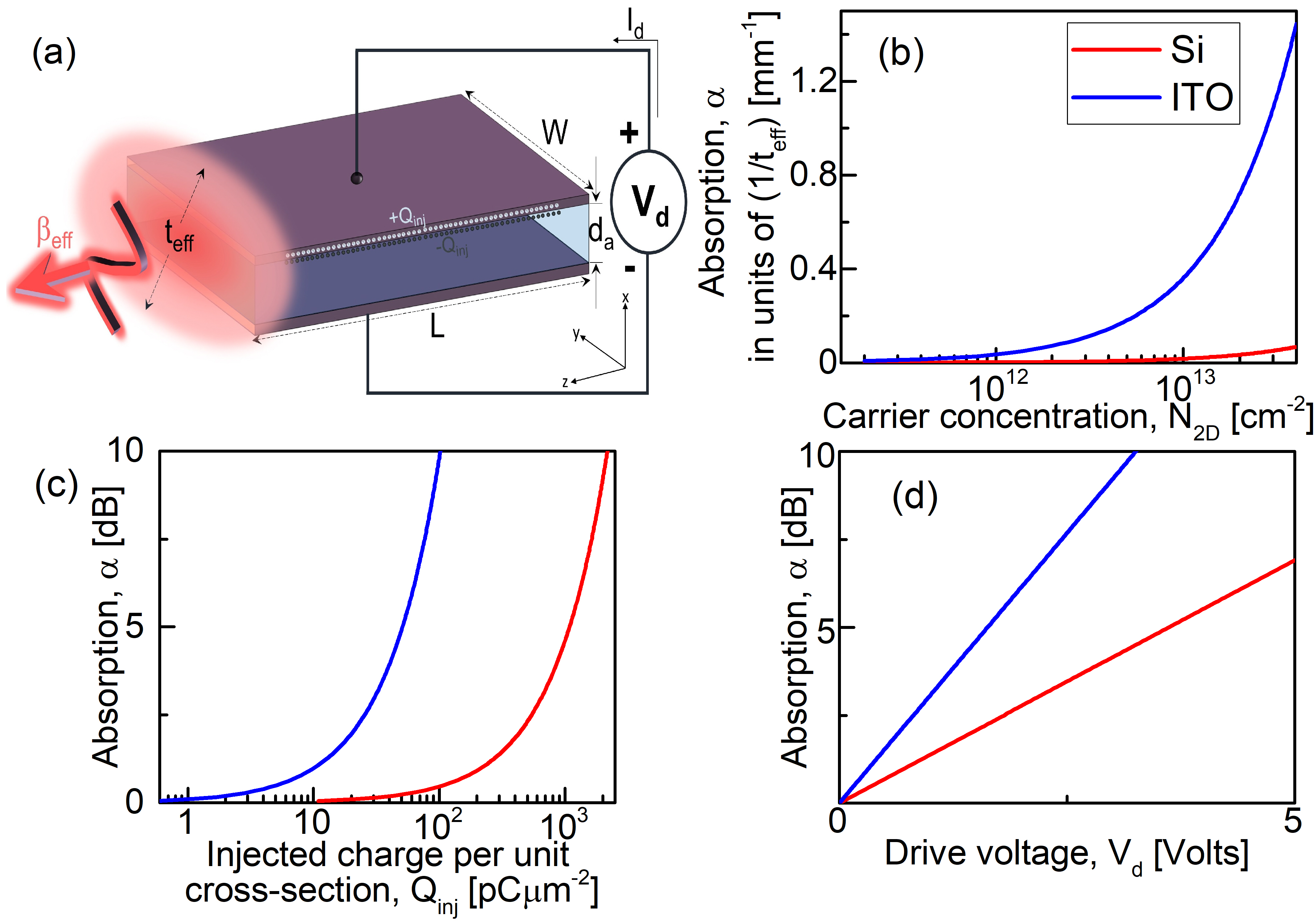
Let us consider a free electron gas in the conduction band of a semiconductor such as in Si, ITO, or any other similar material with the carrier density of . The schematics of a generic waveguide modulator case is shown in Fig. 1(a) employing such active materials. Here, we derive the expression for the absorption cross-section of free electrons in these akin materials. The relative permittivity of aforementioned free electron plasma in the Drude approximation can be written as
| (1) |
where is the dielectric constant of the undoped semiconductor also referred to as the high-frequency or ’background’ permittivity, is the electronic charge, is the conduction effective mass, is the angular frequency, and is the collision frequency of the free carriers quantified by the detuning from any interband resonances thereof. The rate of absorption of electro-magnetic energy is proportional to the imaginary part of the dielectric constant, as
| (2) |
where the effective electric field, is the same as the total field, . Now, let us consider an electromagnetic wave in a waveguide with width , propagating along the z-direction (Fig. 1(a)), with the propagation constant expressed as . We can evaluate the Poynting vector as . According to Maxwell equations . Thus, the time-averaged Poynting vector magnitude is , where is the impedance of free space (377). The effective index has been introduced as . Integrating over the waveguide cross-section (Fig. 1(a)) we obtain
| (3) |
The total power flow then becomes
| (4) |
Here, is defined as the 2-dimensional planar carrier concentration and the effective thickness is
| (5) |
For a very narrow active layer, this approximation can be inferred – otherwise it is slightly smaller. This definition of the effective thickness may differ from many other in the literature, but the difference is not significant. Usually it is just in the arrangement of all kinds of indices. Note, this definition includes the fact that active layer is not necessary at the center of the waveguide, i.e. need not be the peak electric field. The effective thickness can also be thought of as a relative measure of the confinement of the optical mode to the active layer as confinement factor, . Now, we can obtain from (3) as
| (6) |
The absorption coefficient can be found as ; where the absorption cross-section is expressed as
| (7) |
Here, is the fine structure constant, and represents a Lorentzian line shape that has maximum value at resonance equal to unity. The effective detuning then becomes . Note, the maximum absorption is achieved at and when and
| (8) |
Evidently, this expression is similar to the absorption cross section of semiconductor quantum dots (QDs) with one major difference – due to non-resonant character of the free carrier absorption, the cross section for the free carriers is orders of magnitude lower than that for the resonant QDs Amin, Khurgin, and Sorger (2018). As one can see, absorption cross-section does not depend on too many things – at the resonance it depends only to resonance width, or, better and the optical dipole transition rate, . We can invoke the oscillator sum rule (assuming all the dipoles along the axis parallel to the electric field are lined up) which states . Therefore, we can introduce the oscillator strength as and consequentially get
| (9) |
If we now assume that the material used is a semiconductor with a bandgap, and the momentum matrix element quantified by , we can actually relate the effective mass of electron to the wavelength,
| (10) |
where , for a wide range of semiconductors. Therefore, we obtain (assuming that the bandgap is close to the photon energy)
| (11) |
Thus, while modulators based on two-level systems do inherently benefit from the small , the condition for the free carrier absorption based modulators is quite opposite as they benefit from for large . Also, we see that for the wavelength in the telecom range the cross-section actually scales with broadening caused by scattering . Therefore, ITO leads intrinsically to more modulation per unit charge than high-quality Silicon. We found in our previous work, that for all materials operating with Pauli blocking (saturable absorption schemes) show comparable values of absorption cross-section ( at room temperature)Amin, Khurgin, and Sorger (2018), whilst the free carriers offer a worse performance due to non-resonant character of absorption, since according to (8) for free carriers . To verify these analytical results, obtained from essentially perturbative approach, we calculate the dependence of the absorption coefficient on the injected (induced by the gate) carriers, as the elemental free carriers responsible for absorption tuning in the electrostatic modulators as
| (12) |
Here, is the carrier scattering rate i.e. collision frequency with being the mean scattering time corresponding to the mean free path between collisions between the free electrons in the plasma. The electron mobility, and are related by . We compare two free carrier absorption based materials for our absorption modulators to employ in the following neuromorphic study, namely Silicon and ITO. For Si, the conductivity effective mass, is taken as , where is the free electron rest mass Sze and Ng (2006). is taken as 1100 at carrier concentration level (i.e. electrons for Silicon)Nashima et al. (2001). We used the dielectric constant of non-doped silicon = 11.66Holm and Champlin (1968). Unlike the doped silicon, the chemical composition of ITO is usually given as and can be considered an alloy as concentration of Sn relative to In can be as high as 10%. Several previous studies have calculated the permittivity of ITO using the experimentally measured reflectance and transmittance, and we chose a fitting result of Michelotti et. al whereas depends on the deposition conditions, defect states, and film thicknesses, etc.; in our analysis we have taken = 1.8, background permittivity, = 3.9, and Michelotti et al. (2009); Noginov et al. (2011); Vasudev et al. (2013); Naik, Shalaev, and Boltasseva (2013). In the near-infrared, ITO is quasi-metallic since its free electrons dictate its optical response. In fact, ITO and related transparent conducting oxides have recently been explored as plasmonic materials in the optical frequency rangeNoginov et al. (2011); Amin et al. (2018c).
The inherent low broadening parameter, of Si limits the attainable absorption with carrier density level variation even at higher concentrations. More importantly, the slope of absorption vs. density characteristics is responsible for the modulator performance (i.e. slope steepness ), and as such ITO exhibits prominent features as the ITO curve is several orders per decade higher in steepness than the Si one (Fig. 1(b)). Additionally, we evaluate the total absorption as a function of the injected charge per unit waveguide cross-sectional area setting a 10 dB ER ceiling, (Fig. 1(c)). In accordance to our perturbative estimation the injected charge follows Amin, Khurgin, and Sorger (2018). Further, the drive voltage can be obtained via , where is the gate capacitance (Fig. 1(d)). A dielectric spacer, as such, an oxide layer for gating facilitation is considered in these analytical formalism. A gate oxide with a relative dielectric constant, of 10 and gate spacer thickness, of 5 nm was chosen for acquiring these results. As the drive voltage is increased, free carriers leading to dispersive effects are induced and a corresponding net increase occurs in the carrier concentration. While both ITO and Si are capable of tuning the index via the free carrier dependent Drude model, nevertheless ITO exhibits disparate significant advantages over Si with respect to the permittivity variation; firstly, the carrier concentration in ITO can exceed that of Si by at least couple of orders of magnitude; the concentration of indium atoms in ITO reaches a few percent, which is significantly beyond the attainable donor concentration in doped SiAmin et al. (2017). Secondly, the effect of inducing the carrier concentration change in ITO on its refractive index is more dramatic than in Si. This can be attributed to the higher bandgap and consequently lower refractive index of ITO compared to that of Si. The higher bandgap allows the density of states (DoS) near band edge to be tighter confined leading to a higher free carrier concentration necessary to change the index. For a discrete spectrum, the DoS consists of a number of delta peaks at the energy levels of the system with weighted degeneracy of that level. If the change of the carrier concentration (e.g. due to an applied bias) causes a change in the relative permittivity (dielectric constant) , the corresponding change in the refractive index can be written as , hence the refractive index change is greatly enhanced when the permittivity is smallAmin et al. (2018c, b). Third, the presence of an epsilon-near-zero (ENZ) region in the tolerable carrier concentration range within electrostatic gating constraints makes ITO a formidable opponent to conventional Si. Operation in the vicinity of (ENZ) condition can understandably result in stronger modulation effects as the optical mode experiences gradually intensifying slow-light effects closer to the ENZ region as a result of increasing light matter interaction thereof. The inherently low background permittivity of ITO allows the ENZ carrier density condition at telecommunication relevant wavelength of 1550 nm resulting in experimentally obtainable effects Amin et al. (2018c, b, 2017). Interestingly, Si ENZ condition can be approached at a carrier concentration level of about , operating at a wavelength of 10 in the IR region away from the region of our interest.
II.2 Neural Network
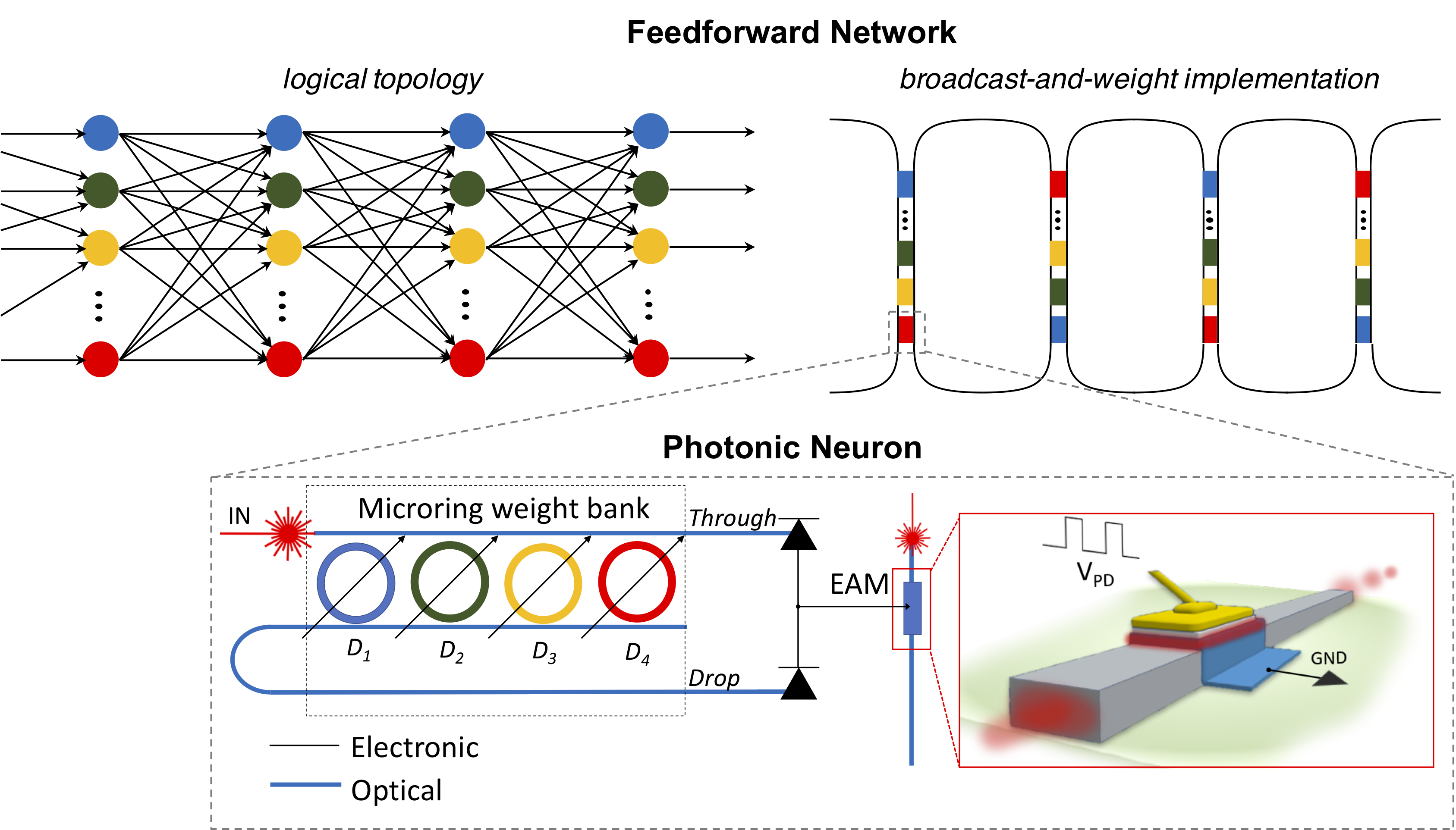
The model of the ITO absorption mechanism is then incorporated in the NL activation function of a neural network. A standard broadcast-and-weight feed-forward network architecture in which connections are configured by microring weight banks Peng et al. (2018), characterized by two layers and 100 nodes per layer, is considered in Fig. 2. The network is trained to classify 10 individual digits in a set of images of handwritten digits in a grayscale 2828 pixel (MNIST dataset LeCun and Cortes (2010)). It is worth noticing, that here each pixel is encoded in unique wavelength carrier in a wavelength division multiplexed (WDM) and broadcast scheme. Subsequently, the network inference performance are benchmarked. The simulation environment was developed in Python using Keras Chollet et al. (2015) and TensorFlow Abadi et al. (2015). The activation function was replaced with a custom designed non linear transfer function resulting from our ab-initio ITO based electro-absorption modulator model. The weighting mechanism relies on microring resonator banks as proposed by Tait et alTait et al. (2017a, 2014), which can potentially support more than 100 channelsTait et al. (2014). In this case, the weights were bound between minus one and one to simulate input optical weighting by rings in a push-pull configuration.
Noise is modeled in Keras as additive Guassian noise with standard deviation proportional to the RMS noise power. Shot noise at the photodiodes is modeled as Where is the signal current and is the dark current taken as 0.05 nA. In addition, thermal noise is modeled as , where is taken as room temperature of 300 K and is the equivalent resistance of .
II.2.1 Training
The neural network models are trained in Keras Chollet et al. (2015) with Adagrad Duchi, Hazan, and Singer (2010) method using a categorical cross-entropy loss function, a learning rate of 0.005, zero decay, with 500 epochs of a 1024 batch size. The amplitude of the noise power model is reduced during training to 10% of the final inference noise power, to allow for training convergence while keeping the model from overfitting to a noiseless activation function.
II.2.2 Parameter Optimization
The photonic neural network differs from the digital neural network in three ways: First, the noise of the photonic neural network is analog, with sources from shot and thermal noise, and unlike the digital neural network has no quantization noise. Second, the photonic neural network, as an analog system, cascades noise. However, unlike an analog repeater, the analog neural network acts as a signal regenerator when the activation function is pushed into saturation, making the analog neural network a quasi-digital system in certain configurations. Finally, the photonic neural network without parameter optimization will shift the bias and dynamic range moving with depth into the network.
To counter-act the shifting bias and dynamic range, an optimization procedure was designed to locate the center and range of the activation function at each layer of the network as follows: the activation function is swept over 200 input voltage points with no noise, the point with the greatest slope is found, a range is built by adding the points to the left and right of the starting point until the slope has dropped below 0.05. After identifying the center of the dynamic range, a DC bias is applied to the modulator to move the minimum input to the center of the identified range.
III Results and Discussion
III.1 ITO electro-absorption activation function: Inference results
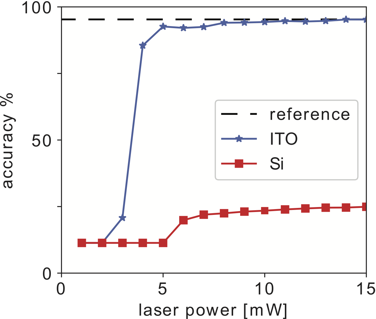
An activation function derived from Eq. (12) for both ITO and Si based absorption modulators coupled to a photodiode (Fig. 2) through an ideal transimpedance amplifier was trained in KerasChollet et al. (2015) at a simulated bandwidth of 1 GHz. The length for both modulators was taken to be the 10 dB dynamic range point for ITO at 1768 in units of the effective thickness, . We keep the scaling independent of the modal structure choice (only material dependent, i.e. Si/ITO) by using the effective thickness as the underlying unit for device length as can be different for different modes but the physical length required for modulation relates back to based on the modal choice as depends only on material constraints (i.e. maximum attainable absorption)Amin, Khurgin, and Sorger (2018). The simulation resulted in accuracy greater than 90% for laser power greater than 5 mW (Fig. 3) for the ITO modulator, while the Si modulator never reached accuracy greater than 30% even at the final sweep power of 15 mW. It is worth noticing that here we compare Si and ITO modulator with the same physical footprint exemplified by the modulator length in effective thickness () to achieve 10 dB modulation for the ITO device. Moreover, as aforementioned in section II.1, this effect is due to the lower modulation range () in Si compared to ITO ascribable to the inherent low effective broadening parameter, of Si which drastically limits the attainable absorption even at higher carrier density levels. As such, similar accuracy level in executing neural network tasks can be obtained for Si based modulators with substantially larger linear footprint compared to ITO-based electro-absorption modulators, when used as nonlinear activation functions. Even with the enhanced footprint, Si based devices could be susceptible to accuracy challenges as opposed to their highly scalable ITO counterparts because of the steep dynamic response of the latter (Fig. 1(d)).
| Material |
|
|
|
|
|
|
||||||||||||
|---|---|---|---|---|---|---|---|---|---|---|---|---|---|---|---|---|---|---|
| LiNbO3Wang et al. (2018) | MZM | 2 | 7000 | 60 | 1700 | 8 | ||||||||||||
| SiPatel et al. (2018) | MZM | 10 | 10500 | 4 | - | - | ||||||||||||
| SiStreshinsky et al. (2013) | MZM | 2 | 3000 | 50 | 450 | 3 | ||||||||||||
| SiLi et al. (2012) | MRR | 3 | 10 | 40 | 80 | 7 | ||||||||||||
| SiPantouvaki et al. (2015) | MRR | 3 | 10 | 56 | 45 | 4 | ||||||||||||
| SiTimurdogan et al. (2014) | MRR | 1 | 5 | 40 | 4 | 8 | ||||||||||||
| This work | EAM | 1 | 5 | 25Kim and Kim (2016) | 60 | 5 |
III.2 Experimental characterization of an ITO based Electro-Absorption Modulator Device
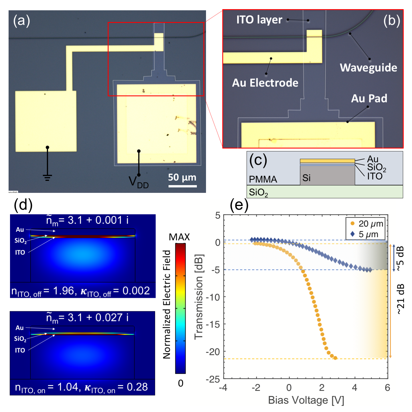
Using the same approach presented in Sorger et al. (2012), we fabricate two different EA modulators with different length (5 and 20 m). The device configuration consists of a Si waveguide (800 nm 340 nm) and stack, placed on top, which comprises of 10 nm ITO layer, gate oxide (SiO2, =20 nm) and a metallic gold pad. The stack was fabricated using electron-beam lithography for defining the pattern, electron-beam evaporation and lift off processing. In this capacitor configuration, according to the potential applied, we are able to modulate the carrier density of the ITO film, thus tuning the portion of the electric field absorbed by the thin layer. A 1550 nm TM mode travelling in the waveguide is subjected to a shift in the mode profile due to the presence of the plasmonic stack, and accordingly enhances the mode overlap with the active ITO layer. Increasing the carrier concentration level with active electro-static gating enhances the modulation effect due to the increased free carrier absorption of the optical mode dynamics as previously discussed. The performances of the characterized electro-absorption modulators display extinction ratios of 5 dB and more than 20 dB for corresponding device lengths of 5 and 20 m, respectively; when a voltage bias between the ITO and the metal contact is applied. The insertion losses are relatively low, and for a device of 5 m are approximately 1 dB. Going beyond the comparison between the proposed device and free carrier absorption in Si modulators, in Table 1 we relate our ITO based EAM to the state-of-the-art Silicon and LiNbO3 based traveling-wave modulators, currently employed in integrated photonic circuits. As can therefore be inferred, the proposed modulator compares also very well with other regularly employed Si and Lithium Niobate state of the art EO modulators. The proposed modulator reaches striking modulation range considering the limited footprint. Moreover, it does not necessitate cavity feedback (eg. micro-ring resonators) and has a broadband response.
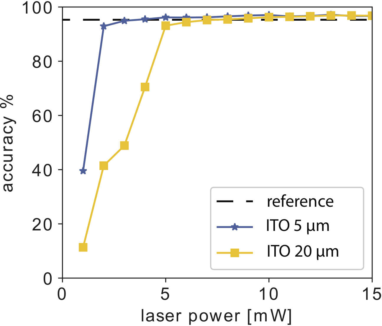
Proceeding further with our analysis, we introduce the experimental EA modulator performance as component of the Nonlinear activation function in the MNIST classifier of handwritten digits Fig. 1 as previously done for our theoretical study. We fit a 10 degree polynomial with saturation to the experimental data (Fig. 5). In this case with the greater performance of the plasmonic mode we modeled an activation function with the modulators capacitively coupled to the photodiodes. In capacitive coupling, the signal is integrated over one clock period and then allowed to modulate for the second clock period. This results in an 5 GHz effective clock rate at a 10 GHz frequency. The results show greater performance of the 5 m ITO modulator over the 20 m ITO modulator for laser power less than 5 mW, while both modulators asymptotically converge to an accuracy greater of 97% as laser power is increased to 15 mW.
IV Conclusions
In conclusion, in this work we described the free carrier absorption dynamics in ITO. The model of the ITO absorption mechanism is then incorporated as NL activation function of a neural network which comprises 2 layer with 100 nodes each. After an accurate multi-parameter optimization, the proposed noise-material capacitor-circuit model shows that the ITO based modulator used as component of the NL activation mechanism can provide high accuracy (up to 97%) in the inference results in neural networks, which implements handwritten classification prediction tasks, with a throughput of of 5 GHz, characterized by low latency and a power budget in the order of less than 10 watts. For the optical platform only, in a trained network, the consumption of one electro-absorption module during the inference phase is assumed approximately to be 60 fJ/bit ( ). At the system level, neglecting I/O and laser power, this translates into 12 pJ/bit (fJ/bit) consumption for the linear activation functions. Moreover, we incorporate in our photonic model of tensor-flow, experimental data of a fabricated ITO based EA modulator, showing even higher performance than the ones predicted by the model, which doesn’t account for device asymmetries and material nonidealities. In our vision, these results make ITO a very competitive material for electro-optic neural network, particularly for implementing nonlinear activation function for low latency and power demanding applications such as communications and LiDAR.
References
- Prucnal and Shastri (2017) P. R. Prucnal and B. J. Shastri, eds., Neuromorphic Photonics, 1st ed. (CRC Press, Boca Raton, FL, 2017).
- Shastri et al. (2018) B. J. Shastri, A. N. Tait, T. F. de Lima, M. A. Nahmias, H.-T. Peng, and P. R. Prucnal, “Principles of neuromorphic photonics,” arXiv:1801.00016 [physics] , 1–37 (2018), arXiv: 1801.00016.
- Shen et al. (2017) Y. Shen, N. C. Harris, S. Skirlo, M. Prabhu, T. Baehr-Jones, M. Hochberg, X. Sun, S. Zhao, H. Larochelle, D. Englund, and M. Soljačić, “Deep learning with coherent nanophotonic circuits,” Nature Photonics 11, 441–446 (2017).
- Heni et al. (2019) W. Heni, Y. Fedoryshyn, B. Baeuerle, A. Josten, C. B. Hoessbacher, A. Messner, C. Haffner, T. Watanabe, Y. Salamin, U. Koch, D. L. Elder, L. R. Dalton, and J. Leuthold, “Plasmonic IQ modulators with attojoule per bit electrical energy consumption,” Nature Communications 10, 1694 (2019).
- Amin et al. (2018a) R. Amin, Z. Ma, R. Maiti, S. Khan, J. B. Khurgin, H. Dalir, and V. J. Sorger, “Attojoule-efficient graphene optical modulators,” Applied Optics 57, D130–D140 (2018a).
- Nozaki et al. (2017) K. Nozaki, A. Shakoor, S. Matsuo, T. Fujii, K. Takeda, A. Shinya, E. Kuramochi, and M. Notomi, “Ultralow-energy electro-absorption modulator consisting of InGaAsP-embedded photonic-crystal waveguide,” APL Photonics 2, 056105 (2017).
- Chiu (2015) Y. Chiu, “Design and fabrication of optical electroabsorption modulator for high speed and high efficiency,” in 2015 14th International Conference on Optical Communications and Networks (ICOCN) (2015) pp. 1–4.
- Ferreira et al. (2017) d. L. T. Ferreira, B. J. Shastri, A. N. Tait, M. A. Nahmias, and P. R. Prucnal, “Progress in neuromorphic photonics,” Nanophotonics 6, 577–599 (2017).
- Brunner et al. (2013) D. Brunner, M. C. Soriano, C. R. Mirasso, and I. Fischer, “Parallel photonic information processing at gigabyte per second data rates using transient states,” Nature Communications 4, 1364 (2013).
- Blumenthal (2018) D. J. Blumenthal, “Integrated combs drive extreme data rates,” Nature Photonics 12, 447 (2018).
- Moscoso-Mártir et al. (2017) A. Moscoso-Mártir, J. Müller, E. Islamova, F. Merget, and J. Witzens, “Calibrated Link Budget of a Silicon Photonics WDM Transceiver with SOA and Semiconductor Mode-Locked Laser,” Scientific Reports 7, 12004 (2017).
- Mehrabian et al. (2018) A. Mehrabian, Y. Al-Kabani, V. J. Sorger, and T. El-Ghazawi, “PCNNA: A Photonic Convolutional Neural Network Accelerator,” arXiv (2018).
- Tait et al. (2014) A. N. Tait, M. A. Nahmias, B. J. Shastri, and P. R. Prucnal, “Broadcast and Weight: An Integrated Network For Scalable Photonic Spike Processing,” Journal of Lightwave Technology 32, 3427–3439 (2014).
- George et al. (2019) J. K. George, A. Mehrabian, R. Amin, J. Meng, T. F. d. Lima, A. N. Tait, B. J. Shastri, T. El-Ghazawi, P. R. Prucnal, and V. J. Sorger, “Neuromorphic photonics with electro-absorption modulators,” Optics Express 27, 5181–5191 (2019).
- Miscuglio et al. (2018) M. Miscuglio, A. Mehrabian, Z. Hu, S. I. Azzam, J. George, A. V. Kildishev, M. Pelton, and V. J. Sorger, “All-optical nonlinear activation function for photonic neural networks [Invited],” Optical Materials Express 8, 3851–3863 (2018).
- Dejonckheere et al. (2014) A. Dejonckheere, F. Duport, A. Smerieri, L. Fang, J.-L. Oudar, M. Haelterman, and S. Massar, “All-optical reservoir computer based on saturation of absorption,” Optics Express 22, 10868 (2014).
- Ma et al. (2017) P. Y. Ma, B. J. Shastri, T. F. de Lima, A. N. Tait, M. A. Nahmias, and P. R. Prucnal, “All-optical digital-to-spike conversion using a graphene excitable laser,” Optics Express 25, 33504 (2017).
- Shastri et al. (2016) B. J. Shastri, M. A. Nahmias, A. N. Tait, A. W. Rodriguez, B. Wu, and P. R. Prucnal, “Spike processing with a graphene excitable laser,” Scientific Reports 6 (2016), 10.1038/srep19126.
- Peng et al. (2018) H. Peng, M. A. Nahmias, T. F. d. Lima, A. N. Tait, and B. J. Shastri, “Neuromorphic Photonic Integrated Circuits,” IEEE Journal of Selected Topics in Quantum Electronics 24, 1–15 (2018).
- Mesaritakis et al. (2016) C. Mesaritakis, A. Kapsalis, A. Bogris, and D. Syvridis, “Artificial Neuron Based on Integrated Semiconductor Quantum Dot Mode-Locked Lasers,” Scientific Reports 6, 39317 (2016).
- Alexander et al. (2013) K. Alexander, T. V. Vaerenbergh, M. Fiers, P. Mechet, J. Dambre, and P. Bienstman, “Excitability in optically injected microdisk lasers with phase controlled excitatory and inhibitory response,” Optics Express 21, 26182–26191 (2013).
- Coarer et al. (2018) F. D. Coarer, M. Sciamanna, A. Katumba, M. Freiberger, J. Dambre, P. Bienstman, and D. Rontani, “All-Optical Reservoir Computing on a Photonic Chip Using Silicon-Based Ring Resonators,” IEEE Journal of Selected Topics in Quantum Electronics 24, 1–8 (2018).
- Cai, Vasudev, and Brongersma (2011) W. Cai, A. P. Vasudev, and M. L. Brongersma, “Electrically controlled nonlinear generation of light with plasmonics,” Science (New York, N.Y.) 333, 1720–1723 (2011).
- Kauranen and Zayats (2012) M. Kauranen and A. V. Zayats, “Nonlinear plasmonics,” Nature Photonics 6, 737–748 (2012).
- Tait et al. (2017a) A. N. Tait, T. F. de Lima, E. Zhou, A. X. Wu, M. A. Nahmias, B. J. Shastri, and P. R. Prucnal, “Neuromorphic silicon photonic networks,” Scientific Reports 7 (2017a), 10.1038/s41598-017-07754-z, arXiv: 1611.02272.
- George et al. (2018) J. George, R. Amin, A. Mehrabian, J. Khurgin, T. El-Ghazawi, P. R. Prucnal, and V. J. Sorger, “Electrooptic Nonlinear Activation Functions for Vector Matrix Multiplications in Optical Neural Networks,” in Advanced Photonics 2018 (BGPP, IPR, NP, NOMA, Sensors, Networks, SPPCom, SOF) (2018), paper SpW4G.3 (Optical Society of America, 2018) p. SpW4G.3.
- Tait et al. (2017b) A. N. Tait, T. F. d. Lima, E. Zhou, A. X. Wu, M. A. Nahmias, B. J. Shastri, and P. R. Prucnal, “Neuromorphic photonic networks using silicon photonic weight banks,” Scientific Reports 7, 7430 (2017b).
- Yoo et al. (2016) S. Yoo, R. Kim, J.-H. Park, and Y. Nam, “Electro-optical Neural Platform Integrated with Nanoplasmonic Inhibition Interface,” ACS Nano 10, 4274–4281 (2016).
- Amin, Khurgin, and Sorger (2018) R. Amin, J. B. Khurgin, and V. J. Sorger, “Waveguide-based electro-absorption modulator performance: comparative analysis,” Optics Express 26, 15445–15470 (2018).
- Oulton et al. (2008) R. F. Oulton, V. J. Sorger, D. A. Genov, D. F. P. Pile, and X. Zhang, “A hybrid plasmonic waveguide for subwavelength confinement and long-range propagation,” Nature Photonics 2, 496–500 (2008).
- Sorger et al. (2012) V. J. Sorger, N. D. Lanzillotti-Kimura, R.-M. Ma, and X. Zhang, “Ultra-compact silicon nanophotonic modulator with broadband response,” Nanophotonics 1, 17–22 (2012).
- Haffner et al. (2018) C. Haffner, D. Chelladurai, Y. Fedoryshyn, A. Josten, B. Baeuerle, W. Heni, T. Watanabe, T. Cui, B. Cheng, S. Saha, D. L. Elder, L. R. Dalton, A. Boltasseva, V. M. Shalaev, N. Kinsey, and J. Leuthold, “Low-loss plasmon-assisted electro-optic modulator,” Nature 556, 483 (2018).
- Keeler et al. (2017) G. A. Keeler, K. M. Geib, D. K. Serkland, S. Parameswaran, T. S. Luk, T. S. Luk, A. J. Griñe, J. Ihlefeld, S. Campione, and J. R. Wendt, “Multi-Gigabit Operation of a Compact, Broadband Modulator Based on ENZ Confinement in Indium Oxide,” in Optical Fiber Communication Conference (2017), paper Th3I.1 (Optical Society of America, 2017) p. Th3I.1.
- Zhu, Lo, and Kwong (2013) S. Zhu, G. Q. Lo, and D. L. Kwong, “Phase modulation in horizontal metal-insulator-silicon-insulator-metal plasmonic waveguides,” Optics Express 21, 8320–8330 (2013).
- Wu et al. (2008) Z. Wu, R. L. Nelson, J. W. Haus, and Q. Zhan, “Plasmonic electro-optic modulator design using a resonant metal grating,” Optics Letters 33, 551–553 (2008).
- Gan et al. (2013) X. Gan, R.-J. Shiue, Y. Gao, K. F. Mak, X. Yao, L. Li, A. Szep, D. Walker, J. Hone, T. F. Heinz, and D. Englund, “High-Contrast Electrooptic Modulation of a Photonic Crystal Nanocavity by Electrical Gating of Graphene,” Nano Letters 13, 691–696 (2013).
- Briggs et al. (2010) R. M. Briggs, J. Grandidier, S. P. Burgos, E. Feigenbaum, and H. A. Atwater, “Efficient Coupling between Dielectric-Loaded Plasmonic and Silicon Photonic Waveguides,” Nano Letters 10, 4851–4857 (2010).
- Lee et al. (2014) H. W. Lee, G. Papadakis, S. P. Burgos, K. Chander, A. Kriesch, R. Pala, U. Peschel, and H. A. Atwater, “Nanoscale Conducting Oxide PlasMOStor,” Nano Letters 14, 6463–6468 (2014).
- Vasudev et al. (2013) A. P. Vasudev, J.-H. Kang, J. Park, X. Liu, and M. L. Brongersma, “Electro-optical modulation of a silicon waveguide with an “epsilon-near-zero” material,” Optics Express 21, 26387–26397 (2013).
- Babicheva, Boltasseva, and Lavrinenko (2015) V. E. Babicheva, A. Boltasseva, and A. V. Lavrinenko, “Transparent conducting oxides for electro-optical plasmonic modulators,” Nanophotonics 4, 165–185 (2015).
- Abdelatty, Badr, and Swillam (2018) M. Y. Abdelatty, M. M. Badr, and M. A. Swillam, “Hybrid plasmonic electro-optical absorption modulator based on epsilon-near-zero characteristics of ITO,” in Integrated Optics: Devices, Materials, and Technologies XXII, Vol. 10535 (International Society for Optics and Photonics, 2018) p. 105351T.
- Alam, Leon, and Boyd (2016) M. Z. Alam, I. D. Leon, and R. W. Boyd, “Large optical nonlinearity of indium tin oxide in its epsilon-near-zero region,” Science 352, 795–797 (2016).
- Zhao et al. (2014) H. Zhao, Y. Wang, A. Capretti, L. D. Negro, and J. Klamkin, “Silicon photonic modulators based on epsilon-near-zero indium tin oxide materials,” in 2014 IEEE Photonics Conference (2014) pp. 334–335.
- noa (2008) “US8049862b2 - Indium tin oxide (ITO) layer forming - Google Patents,” (2008).
- Kerkache et al. (2006) L. Kerkache, A. Layadi, E. Dogheche, and D. Rémiens, “Physical properties of RF sputtered ITO thin films and annealing effect,” Journal of Physics D: Applied Physics 39, 184 (2006).
- Chityuttakan et al. (2019) C. Chityuttakan, P. Chinvetkitvanich, S. Chatraphorn, and S. Chatraphorn, “Influence of deposition parameters on the quality of ITO films for photovoltaic application,” AIP Conference Proceedings 2091 , 3 (2019).
- Hu et al. (2004) Y. Hu, X. Diao, C. Wang, W. Hao, and T. Wang, “Effects of heat treatment on properties of ITO films prepared by rf magnetron sputtering,” Vacuum 75, 183–188 (2004).
- Bhatti, Rana, and Khan (2004) M. T. Bhatti, A. M. Rana, and A. F. Khan, “Characterization of rf-sputtered indium tin oxide thin films,” Materials Chemistry and Physics 84, 126–130 (2004).
- Lee and Ok Park (2004) H.-C. Lee and O. Ok Park, “Behaviors of carrier concentrations and mobilities in indium–tin oxide thin films by DC magnetron sputtering at various oxygen flow rates,” Vacuum 77, 69–77 (2004).
- Amin et al. (2018b) R. Amin, R. Maiti, C. Carfano, Z. Ma, M. H. Tahersima, Y. Lilach, D. Ratnayake, H. Dalir, and V. J. Sorger, “0.52 V mm ITO-based Mach-Zehnder modulator in silicon photonics,” APL Photonics 3, 126104 (2018b).
- Gui et al. (2018) Y. Gui, M. Miscuglio, Z. Ma, M. T. Tahersima, S. Sun, R. Amin, H. Dalir, and V. J. Sorger, “Towards integrated metatronics: a holistic approach on precise optical and electrical properties of Indium Tin Oxide,” arXiv (2018).
- Tang, Peters, and Bowers (2012) Y. Tang, J. D. Peters, and J. E. Bowers, “Over 67 GHz bandwidth hybrid silicon electroabsorption modulator with asymmetric segmented electrode for 1.3 m transmission,” Optics Express 20, 11529–11535 (2012).
- Tu et al. (2011) X. Tu, T.-Y. Liow, J. Song, M. Yu, and G. Q. Lo, “Fabrication of low loss and high speed silicon optical modulator using doping compensation method,” Optics Express 19, 18029–18035 (2011).
- Soref and Bennett (1987) R. Soref and B. Bennett, “Electrooptical effects in silicon,” IEEE Journal of Quantum Electronics 23, 123–129 (1987).
- Reed et al. (2013) G. T. Reed, G. Z. Mashanovich, F. Y. Gardes, M. Nedeljkovic, Y. Hu, D. J. Thomson, K. Li, P. R. Wilson, S.-W. Chen, and S. S. Hsu, “Recent breakthroughs in carrier depletion based silicon optical modulators,” Nanophotonics 3, 229–245 (2013).
- Haffner et al. (2015) C. Haffner, W. Heni, Y. Fedoryshyn, J. Niegemann, A. Melikyan, D. L. Elder, B. Baeuerle, Y. Salamin, A. Josten, U. Koch, C. Hoessbacher, F. Ducry, L. Juchli, A. Emboras, D. Hillerkuss, M. Kohl, L. R. Dalton, C. Hafner, and J. Leuthold, “All-plasmonic Mach–Zehnder modulator enabling optical high-speed communication at the microscale,” Nature Photonics 9, 525–528 (2015).
- Sze and Ng (2006) S. M. Sze and K. K. Ng, Physics of Semiconductor Devices (John Wiley & Sons, 2006) google-Books-ID: o4unkmHBHb8C.
- Nashima et al. (2001) S. Nashima, O. Morikawa, K. Takata, and M. Hangyo, “Measurement of optical properties of highly doped silicon by terahertz time domain reflection spectroscopy,” Applied Physics Letters 79, 3923–3925 (2001).
- Holm and Champlin (1968) J. D. Holm and K. S. Champlin, “Microwave Conductivity of Silicon and Germanium,” Journal of Applied Physics 39, 275–284 (1968).
- Michelotti et al. (2009) F. Michelotti, L. Dominici, E. Descrovi, N. Danz, and F. Menchini, “Thickness dependence of surface plasmon polariton dispersion in transparent conducting oxide films at 1.55 m,” Optics Letters 34, 839–841 (2009).
- Noginov et al. (2011) M. A. Noginov, L. Gu, J. Livenere, G. Zhu, A. K. Pradhan, R. Mundle, M. Bahoura, Y. A. Barnakov, and V. A. Podolskiy, “Transparent conductive oxides: Plasmonic materials for telecom wavelengths,” Applied Physics Letters 99, 021101 (2011).
- Naik, Shalaev, and Boltasseva (2013) G. V. Naik, V. M. Shalaev, and A. Boltasseva, “Alternative Plasmonic Materials: Beyond Gold and Silver,” Advanced Materials 25, 3264–3294 (2013).
- Amin et al. (2018c) R. Amin, M. H. Tahersima, Z. Ma, C. Suer, K. Liu, H. Dalir, and V. J. Sorger, “Low-loss tunable 1d ITO-slot photonic crystal nanobeam cavity,” Journal of Optics 20, 054003 (2018c).
- Amin et al. (2017) R. Amin, C. Suer, Z. Ma, I. Sarpkaya, J. B. Khurgin, R. Agarwal, and V. J. Sorger, “A deterministic guide for material and mode dependence of on-chip electro-optic modulator performance,” Solid-State Electronics 136, 92–101 (2017).
- LeCun and Cortes (2010) Y. LeCun and C. Cortes, “MNIST handwritten digit database,” http://yann.lecun.com/exdb/mnist/ (2010).
- Chollet et al. (2015) F. Chollet et al., “Keras,” https://keras.io (2015).
- Abadi et al. (2015) M. Abadi, A. Agarwal, P. Barham, E. Brevdo, Z. Chen, C. Citro, G. S. Corrado, A. Davis, J. Dean, M. Devin, S. Ghemawat, I. Goodfellow, A. Harp, G. Irving, M. Isard, Y. Jia, R. Jozefowicz, L. Kaiser, M. Kudlur, J. Levenberg, D. Mané, R. Monga, S. Moore, D. Murray, C. Olah, M. Schuster, J. Shlens, B. Steiner, I. Sutskever, K. Talwar, P. Tucker, V. Vanhoucke, V. Vasudevan, F. Viégas, O. Vinyals, P. Warden, M. Wattenberg, M. Wicke, Y. Yu, and X. Zheng, “TensorFlow: Large-scale machine learning on heterogeneous systems,” (2015), software available from tensorflow.org.
- Duchi, Hazan, and Singer (2010) J. Duchi, E. Hazan, and Y. Singer, “Adaptive subgradient methods for online learning and stochastic optimization,” Tech. Rep. UCB/EECS-2010-24 (EECS Department, University of California, Berkeley, 2010).
- Wang et al. (2018) C. Wang, M. Zhang, B. Stern, M. Lipson, and M. Loncar, “Nanophotonic lithium niobate electro-optic modulators,” Optics Express 26, 1547–1555 (2018).
- Patel et al. (2018) D. Patel, M. Parvizi, N. Ben-Hamida, C. Rolland, and D. V. Plant, “Frequency response of dual-drive silicon photonic modulators with coupling between electrodes,” Optics Express 26, 8904 (2018).
- Streshinsky et al. (2013) M. Streshinsky, R. Ding, Y. Liu, A. Novack, Y. Yang, Y. Ma, X. Tu, E. K. S. Chee, A. E.-J. Lim, P. G.-Q. Lo, T. Baehr-Jones, and M. Hochberg, “Low power 50 Gb/s silicon traveling wave Mach-Zehnder modulator near 1300 nm,” Optics Express 21, 30350 (2013).
- Li et al. (2012) G. Li, X. Zheng, H. Thacker, J. Yao, Y. Luo, I. Shubin, K. Raj, J. E. Cunningham, and A. V. Krishnamoorthy, “40 Gb/s thermally tunable CMOS ring modulator,” in The 9th International Conference on Group IV Photonics GFP (IEEE, San Diego, CA, USA, 2012) pp. 1–3.
- Pantouvaki et al. (2015) M. Pantouvaki, P. Verheyen, J. De Coster, G. Lepage, P. Absil, and J. Van Campenhout, “56gb/s ring modulator on a 300mm silicon photonics platform,” in 2015 European Conference on Optical Communication (ECOC) (IEEE, Valencia, Spain, 2015) pp. 1–3.
- Timurdogan et al. (2014) E. Timurdogan, C. M. Sorace-Agaskar, J. Sun, E. Shah Hosseini, A. Biberman, and M. R. Watts, “An ultralow power athermal silicon modulator,” Nature Communications 5, 4008 (2014).
- Kim and Kim (2016) J.-S. Kim and J. T. Kim, “Silicon electro-optic modulator based on an ITO-integrated tunable directional coupler,” Journal of Physics D: Applied Physics 49, 075101 (2016).