Graphene epsilon-near-zero plasmonic crystals
Abstract.
Plasmonic crystals are a class of optical metamaterials that consist of engineered structures at the sub-wavelength scale. They exhibit optical properties that are not found under normal circumstances in nature, such as negative-refractive-index and epsilon-near-zero (ENZ) behavior. Graphene-based plasmonic crystals present linear, elliptical, or hyperbolic dispersion relations that exhibit ENZ behavior, normal or negative-index diffraction. The optical properties can be dynamically tuned by controlling the operating frequency and the doping level of graphene. We propose a construction approach to expand the frequency range of the ENZ behavior. We demonstrate how the combination of a host material with an optical Lorentzian response in combination with a graphene conductivity that follows a Drude model leads to an ENZ condition spanning a large frequency range.
1. Introduction
The control of electromagnetic (EM) properties of optical materials on the nanoscale has opened the door for designing novel devices and applications that include nano-antennas with extremely short wavelength resonance (Dorfmuller et al., 2010), optical holography (Wintz et al., 2015), and wireless nanocommunication (Jornet and Cabellos, 2015; Hassan et al., 2019). Controlling the structure of materials at the sub-wavelength scale enables the design of metamaterials that possess properties that are not found under normal circumstances in nature such as negative refraction (High et al., 2015) and epsilon-near-zero (ENZ) behavior (Silveirinha and Engheta, 2006). One of the key ingredients for designing such metamaterials is the creation of EM waves with much shorter wavelengths than those of the incident light. These sub-wavelength waves involve electronic motion (plasmons) coupled with EM surface waves and are referred to as surface plasmon polaritons (Jablan et al., 2009; Grigorenko et al., 2012).
Plasmonic crystals are a class of metamaterials that is of particular interest. They consist of metallic layers arranged periodically with sub-wavelength distance in a dielectric host. This class of metamaterials offers fine control of EM properties and can serve as ENZ (Mattheakis et al., 2016; Maier et al., 2018) and negative refractive index media (Wang et al., 2012). ENZ metamaterials exhibit properties which cannot be obtained by traditional photonic systems. These features include wave propagation with no phase delay and diffraction, decoupling of spatial and temporal field variations, propagation through very narrow channels, and ultra fast phase transitions (Silveirinha and Engheta, 2006; Mattheakis et al., 2016). Many novel optical devices have been proposed indicating the broad prospects of the ENZ effect (Huang et al., 2011; Li et al., 2015; Alam et al., 2018). However, novel metals have the unfortunate side effect that their use in plasmonic platforms restricts the frequency range where above exotic optical effects occur. In addition, the resulting plasmonic device regularly suffers from high optical losses and construction defects yield non perfect planar layers which also negatively affect the optical properties. All of these issues may no longer be critical due to the discovery of truly two-dimensional (2D) materials, such as graphene, black phosphorus, hexagonal boron nitride, and molybdenum disulfide. They promise a new era of control of optical properties of photonic and plasmonic devices (Low et al., 2014; Dai et al., 2015; Nemilentsau et al., 2016; Xia et al., 2014; Valagiannopoulos et al., 2017). In particular, graphene supports plasmons with ultra-sub-wavelength behavior, ranging from terahertz (THz) to infrared frequencies. Due to the confining of electrons in two dimensions, the quantum effects are very pronounced and thus 2D materials pose exceptional optical properties and high quantum efficiency for light-matter interaction (Jablan et al., 2009; Grigorenko et al., 2012).
Graphene is a quite interesting material because it allows control of electronic and, in turn, plasmonic properties by changing the density of the free charge carriers through an external gate field, chemical deposition, or intercalation (Grigorenko et al., 2012; Xia et al., 2014; Shirodkar et al., 2018). It has been shown that graphene plasmonic crystals can serve as an ingredient in a tunable metamaterial (Mattheakis et al., 2016; Maier et al., 2018; Wang et al., 2012). In particular, a plasmonic crystal consisting of periodically stacked graphene layers embedded in a dielectric host leads to negative refraction and ENZ behavior in the THZ and infrared frequencies, and allows to tune optical properties by controlling the operation frequency or the doping amount (Mattheakis et al., 2016). It has been furthermore shown that the ENZ condition coincides with a plasmonic Dirac cone in the wavenumber space, where the plasmonic Dirac cone is formed by two asymptotically linear, intersecting dispersion bands (Mattheakis et al., 2016; Maier et al., 2018; Huang et al., 2011; Li et al., 2015). Such a graphene-based plasmonic crystal design, however, has the major shortcoming that ENZ behavior can only be observed for a very small frequency range. This is due to the fact that a plasmonic crystal with a dielectric host that has frequency independent optical properties admits only a single plasmonic Dirac point which restricts the ENZ effect to a very narrow frequency range. This is disadvantageous for a number of optical applications involving a continuous spectrum of EM waves. In this letter we introduce a further degree of freedom in controlling the optical properties of graphene plasmonic crystals by using Lorentz dispersive dielectric host materials (Kittel, 2005). The dielectric function of this family of materials depends on the operating frequency. We find that by using an appropriate Lorentz host we obtain multiple plasmonic Dirac points resulting in a wide frequency range exhibiting an ENZ effect. For a particular host material that we examine, Magnesium Oxide, we demonstrate that (a) two Dirac points emerge in the THz band; and (b) that for a large frequency interval containing the two Dirac points the ENZ condition is fulfilled. As a second design example, we propose a hypothetical dielectric with two Lorentz resonances leading to three Dirac points and an even wider frequency spectrum of ENZ behavior. This example is motivated by the significant progress that was made in (atomistic) material engineering recently, that has the prospect of enabling the engineering of materials with desirable electronic properties. For instance, Van der Waals heterostructures are comprised of different 2D materials that are stacked in a particular way to provide desirable electronic and optical features (Geim and Grigorieva, 2013; Novoselov et al., 2016).
The remainder of this paper is organized as follows. In Section 2 we review the graphene-based plasmonic crystal by using Bloch theory and discuss the mathematical relation between the plasmonic Dirac point and ENZ effect. In Section 3 we extend the frequency range of the ENZ effect by introducing Lorentz materials as the ambient material of the graphene layers. The paper concludes in Section 4 with a summary of the key ideas introduced in this letter and an outlook.
2. Bloch-wave Theory
We consider a plasmonic crystal that consists of a dielectric host surrounding flat in which periodic 2D metallic sheets that are parallel to the -plane located at , for integer . Here, denotes the structural period. The metallic sheets are described by an isotropic surface conductivity . The dielectric host is considered to be an anisotropic material described by a uniaxial dielectric tensor with out-of-plane component and -dependent in-plane components ; the vacuum permittivity is set to unity, . We examine transverse-magnetic (TM) time-harmonic waves with electric and magnetic field components and , respectively. Imposing the rotational symmetry of the crystal and the TM polarization in Maxwell equations yield fields which are translation invariant along direction with guided modes align along direction (Mattheakis et al., 2016), hence
where is the wavenumber along direction. The above assumptions allow us to simplify the system of time dependent Maxwell equations to a one dimensional eigenvalue problem (Maier et al., 2018) with the Helmholtz type governing equation
| (1) |
where , is the angular operating frequency and denotes the ordinary operating frequency, is the free space speed of light. The metallic 2D sheets carry a surface current that acts as a boundary. Maxwell equations dictate that on the boundaries that are defined by the metallic sheets at , the tangential electric field must be continuous with discontinuous derivative with a jump discontinuity due to the surface currents on the metallic plates, hence the transmission conditions are (Maier et al., 2018):
| (2) |
where denotes the limit above and below of a metallic boundary. We can get a closed system of equations by using the Bloch-wave ansatz (Mattheakis et al., 2016; Maier et al., 2018) in the direction with indicating the real Bloch number:
| (3) |
The combination of the transmission conditions (2) and Bloch ansatz (3) yields a closed system of boundary conditions, viz.,
| (4) |
Here, denotes the derivative of with respect to . In order to solve the differential equation (1) with boundary conditions (4) we introduce the two fundamental solutions and of (1) that fulfill the initial conditions:
By substituting a linear combination into (4) we obtain
This system admits a nontrivial solution (with , or ) whenever
| (5) |
Equation now forms a dispersion relation between and . It is convenient to work in a 2D wavenumber space . In Ref. (Maier et al., 2018) formula (5) is used to determine the dispersion relation for several examples of dielectric functions, , including constant, parabolic, double-well, and nonsymmetric dielectric profiles. The plasmonic crystal has the character of an ENZ medium for values in the vicinity of the Dirac point (Maier et al., 2018), that occurs at the center of the Brillouin zone (Mattheakis et al., 2016). It has been shown that the occurence of the plasmonic Dirac point is a universal behavior of 2D plasmonic crystals with any spatial dependence on the dielectric host along the direction (Maier et al., 2018).
At the effective in-plane permittivity component, , of the metamaterial becomes zero, hence in the neighborhood of we observe ENZ behavior. For the purpose of examining ENZ frequency bands in the following, we make the heuristic definition of speaking of an ENZ behavior whenever . In this letter we focus on the frequency-dependent response of a plasmonic crystal assuming that the host material is described by a constant in space but possibly dependent permittivity. Thus, as a last preparatory step we solve the dispersion relation explicitly for the special case of spatially constant and . In this case the fundamental solutions of the differential equation (1) are given by
Substituting both solutions into dispersion relation (5) yields
| (6) |
where
| (7) |
is the plasmonic thickness that determines the length scale of plasmonic structures perpendicular to the 2D material sheets (Mattheakis et al., 2016; Maier et al., 2018; Wang et al., 2012). For close to the dispersion relation (6) reduces to
This implies that up to first order the effective permittivity is given by
| (8) |
It can be shown by a refined argument that equation (8) is universal (Maier et al., 2019): An EM wave traveling through the plasmonic crystal sees an effective homogeneous medium with effective permittivity . Therefore, three distinct cases of wave propagation are possible: elliptic propagation (), hyperbolic propagation (), and ENZ behavior (). The elliptical dispersion bands yield propagating waves with normal diffraction, whereas the hyperbolic bands correspond to negative refraction. The ENZ case is described by a linear Dirac dispersion and corresponds to propagation without dispersion and phase delay (Mattheakis et al., 2016).
Equation (8) provides a systematic way to design plasmonic crystals with ENZ properties. We observe that we obtain when , hence for a given we can tune the plasmonic thickness, , to be equal to , and vice versa. This also explains why graphene is such an exceptional plasmonic platform. The surface conductivity of graphene depends on the operating frequency as well as the doping, hence we can dynamically tune the surface conductivity to achieve . More precisely, the surface conductivity of graphene is given by Kubo’s formula which includes both interband and intraband electronic transitions. Nevertheless, in THz and infrared frequencies the intraband transitions dominate and thus, Kubo’s formula is simplified to Drude model (Jablan et al., 2009; Grigorenko et al., 2012):
| (9) |
where is the Fermi level associating with the density of electric carriers and corresponding to the electronic doping; the can be dynamically tuned by an external gate field or can be fixed by chemical deposition or intercalation (Grigorenko et al., 2012; Xia et al., 2014; Shirodkar et al., 2018). The electron charge is denoted by , is the reduced Planck constant, and is electronic relation time accounting for optical losses with a typically value of ps.
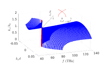
As a first example we study a plasmonic crystal that consists of doped graphene layers in a silica glass host with constant and equal permittivity components of . In Figure 1 we show the dispersion relation calculated by equation (6) for different values of frequency in the range THz. The structural period and the Fermi level are kept constant at nm and eV, respectively. We observe one plasmonic Dirac point that appears at THz (highlighted by red and shown in inset diagram of Figure 1), where the dispersion bands change from elliptical to hyperbolic.
3. Lorentz host material
In the previous section we saw how a (single) plasmonic Dirac point can appear in the dispersion of a 2D metal-based plasmonic crystal that then—in the vicinity of the Dirac point—behaves as an ENZ medium. The ENZ effect is, however, restricted to a narrow range of frequencies. This is an issue for real applications that typically involve a range of operating frequencies forming a wavepacket. We now introduce a Lorentz host material into the plasmonic crystal. We demonstrate how this leads to multiple Dirac points in the dispersion relation and consequently a significantly expanded frequency range with ENZ behavior.
The Drude model takes only intraband electronic transition into account that model free electrons in a metal response to an EM field. Dielectric materials, however, do not have free charge carriers (electrons). Here, the optical response due to an external EM field is mainly caused by bound charges in the dielectric material where radiation can be absorbed due to interband electronic transitions. The Lorentz model is a phenomenological model that takes these interband electronic transitions into account. Dielectrics described by this model are called Lorentz dispersive materials (Kittel, 2005). The contribution of the interband transition leads to a frequency dependent permittivity that reads
| (10) |
Here, denotes the resonance (natural) angular frequency of the bound electrons, is the electron damping rate, and are the high and low frequency limits of the permittivity, respectively.
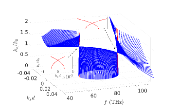
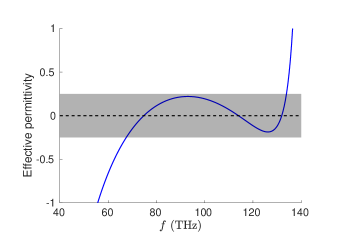
A concrete example for a plasmonic crystal with a Lorentz dispersive host material that shows an extended ENZ band is Magnesium Oxide (MO). MO’s parameters for the Lorentz model read: , , eV ( THz), and (Horiba, 2006). We point out that MO is considered to be a lossless dielectric and hence can be used for optical devices. We compute the dispersion relation (6) of the plasmonic crystal for this case by setting the host permittivity to . The resulting dispersion relation involving and the operating frequency are shown in Figure 2 (upper). We indeed observe two Dirac points at frequencies THz and THz. The two Dirac cones are marked in red in the diagrams and pointed out in the inset of Figure 2.
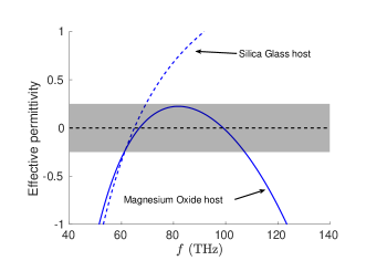
Since we are interested in the ENZ range, we calculate the in-plane effective dielectric permittivity given by equation (8). The results are shown in the lower panel of Figure 2. In particular, we compute the as a function of the frequency for our example of a plasmonic crystal with MO host. For the sake of comparison we plot the for a plasmonic crystal that was studied in previous sections, that it, with silica glass as dielectric host instead of MO. The shaded area represents the ENZ range (). We observe that indeed the ENZ band of the plasmonic crystal with Lorentz dispersive host is significantly extended, about four times, compared to the previous example of a constant permittivity host material.
We can further generalize our approach by assuming dielectric materials with permittivity given by a multi-oscillators Lorentz model (Kittel, 2005) where many interband transitions take place and drastically contribute to the dielectric function. Such a material provides many Dirac points in the space. Subsequently, the becomes zero many times and thus, the ENZ frequency range is significantly expanded. We propose this hypothetical scenario due to the great progress of the material engineering where new materials with desirable electronic properties can be designed in purpose. The Lorentz model that includes multiple oscillators is
| (11) |
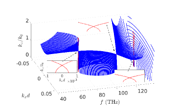
where is the number of the oscillators each one has resonance frequency , damping factor , and strength . Here, we consider a two-oscillator () Lorentz material with the parameters: , , and eV. Thence, we calculate the dispersion relation in ( and present the results in Figure 3 (upper) where we observe three Dirac points at the frequencies THz. In the lower panel of the same figure we outline the effective permittivity in frequency where the ENZ band has been significantly expanded in a range over than THz that is approximately eight times wider range compared to the example of a constant permittivity host material.
4. Conclusion
Metamaterials are artificial structures that manipulate electromagnetic waves on a sub-wavelength scale and provide optical properties that are not found in nature under normal conditions, such as negative refraction and epsilon-near-zero behavior. ENZ metamaterials exhibit exotic properties that include wave propagation through very narrow channels without diffraction and phase delay. Plasmonic crystals are a particular class of metamaterials that consist of periodically arranged metallic layers with distances shorter than the (free space) wavelength. Graphene-based plasmonic crystals are tunable metamaterials since their optical properties can be dynamically tuned by controlling the operating frequency and the electronic doping in graphene. Fine tuning a graphene-based plasmonic crystal yields ENZ behavior in terahertz and infrared frequencies. The appearance of ENZ condition coincides with a plasmonic Dirac cone in the wavenumber space and thus, Dirac points determine the neighborhood where the metamaterial behaves as an ENZ media.
Using an ordinary dielectric as the host material of the plasmonic crystal yields a single Dirac point restricting the ENZ effect to a very narrow frequency range. This may be a critical issue for for real applications that typically involve a range of operating frequencies forming a wavepacket. In this paper we proposed a modified design that expands the frequency range of the ENZ behavior. We replaced the host dielectric in the plasmonic crystal with a Lorentz dispersive material which has a frequency dependent permittivity. We demonstrated that the combination of doped graphene and Lorentz materials yield multiple Dirac points and, subsequently, achieved an ENZ effect over a relatively large frequency range.
Acknowledgements.
We acknowledge partial support from EFRI 2-DARE NSF Grant No. 1542807 (MMat, EK); and ARO MURI Award No. W911NF14-0247 (MMat, MMai, EK). This project was partially supported by the University of Minnesota’s Undergraduate Research Opportunities Program (WXB).References
- (1)
- Alam et al. (2018) M. Z. Alam, S. A. Schulz, J. Upham, I. De Leon, and R. W. Boyd. 2018. Large optical nonlinearity of nanoantennas coupled to an epsilon-near-zero material. Nature Photonics 12 (2018), 79 – 83.
- Dai et al. (2015) S. Dai, Q. Ma, M. K. Liu, T. Andersen, Z. Fei, M. D. Goldflam, M. Wagner, K. Watanabe, T. Taniguchi, M. Thiemens, F. Keilmann, G. C. A. M. Janssen, S-E. Zhu, P. Jarillo-Herrero, M. M. Fogler, and D. N. Basov. 2015. Graphene on hexagonal boron nitride as a tunable hyperbolic metamaterial. Nat. Nano 10, 8 (2015), 682–686.
- Dorfmuller et al. (2010) J. Dorfmuller, R. Vogelgesang, W. Khunsin, C. Rockstuhl, Ch. Etrich, and K. Kern. 2010. Plasmonic Nanowire Antennas: Experiment, Simulation, and Theory. Nano Letters 12 (2010), 3596–3603.
- Geim and Grigorieva (2013) A. K. Geim and I. V. Grigorieva. 2013. Van der Waals heterostructures. Nature 499 (2013), 419–425.
- Grigorenko et al. (2012) A. N. Grigorenko, M. Polini, and K. S. Novoselov. 2012. Graphene plasmonics. Nat. Photon 6 (Oct 2012), 749–758. Issue 11.
- Hassan et al. (2019) N. Hassan, M. Mattheakis, and M. Ding. 2019. Sensorless Node Architecture for Events detection in Self-Powered Nanosensor Networks. Nano Communication Networks 19 (2019), 1 – 9.
- High et al. (2015) A. A. High, R. C. Devlin, A. Dibos, M. Polking, D. S. Wild, J. Perczel, N. P. de Leon, M. D. Lukin, and H. Park. 2015. Visible-frequency hyperbolic metasurface. Nature 522 (Jun 2015), 192–196. Issue 7555.
- Horiba (2006) J. Y. Horiba. 2006. Lorentz Dispersion Model. Technical notes, spectroscopic ellipsometry (2006).
- Huang et al. (2011) X. Huang, Y. Lai, Z. H. Hang, H. Zheng, and C. T. Chan. 2011. Dirac cones induced by accidental degeneracy in photonic crystals and zero-refractive-index materials. Nat. Mater. 10 (2011), 582–586.
- Jablan et al. (2009) M. Jablan, H. Buljan, and M. Soljačić. 2009. Plasmonics in graphene at infrared frequencies. Phys. Rev. B 80 (Dec 2009), 245435. Issue 24.
- Jornet and Cabellos (2015) J. Miquel Jornet and A. Cabellos. 2015. On the feeding mechanisms for graphene-based THz plasmonic nano-antennas. 2015 IEEE 15th International Conference on Nanotechnology (IEEE-NANO) (2015), 168–171.
- Kittel (2005) Charles Kittel. 2005. Introduction to solid state physics (8th ed.). John Wiley and Sons, Inc.
- Li et al. (2015) Y. Li, S. Kita, P. Munoz, O. Reshef, D. I. Vulis, M. Yin, M. Loncar, and E. Mazur. 2015. On-chip zero-index metamaterials. Nat. Photon 9 (Oct 2015), 738–742. Issue 11.
- Low et al. (2014) T. Low, R. Roldán, H. Wang, F. Xia, P. Avouris, L. Martín-Moreno, and F. Guinea. 2014. Plasmons and Screening in Monolayer and Multilayer Black Phosphorus. Phys. Rev. Lett. 113 (Sep 2014), 106802. Issue 10.
- Maier et al. (2018) M. Maier, M. Mattheakis, E. Kaxiras, M. Luskin, and D. Margetis. 2018. Universal behavior of a dispersive Dirac cone in gradient-index plasmonic metamaterials. Phys. Rev. B 97 (Jan 2018), 035307. Issue 3.
- Maier et al. (2019) M. Maier, M. Mattheakis, E. Kaxiras, M. Luskin, and D. Margetis. 2019. Homogenization of plasmonic crystals: Seeking the epsilon-near-zero effect. Submitted (2019). https://arxiv.org/abs/1809.08276
- Mattheakis et al. (2016) M. Mattheakis, C. A. Valagiannopoulos, and E. Kaxiras. 2016. Epsilon-near-zero behavior from plasmonic Dirac point: Theory and realization using two-dimensional materials. Physical Review B 94 (2016), 201404(R).
- Nemilentsau et al. (2016) A. Nemilentsau, T. Low, and G. Hanson. 2016. Anisotropic 2D Materials for Tunable Hyperbolic Plasmonics. Phys. Rev. Lett. 116 (Feb 2016), 066804. Issue 6.
- Novoselov et al. (2016) K. S. Novoselov, A. Mishchenko, A. Carvalho, and A. H. Castro Neto. 2016. 2D materials and van der Waals heterostructures. Science 353, 6298 (2016).
- Shirodkar et al. (2018) S. N. Shirodkar, M. Mattheakis, P. Cazeaux, P. Narang, M. Soljačić, and E. Kaxiras. 2018. Quantum plasmons with optical-range frequencies in doped few-layer graphene. Phys. Rev. B 97 (May 2018), 195435. Issue 19.
- Silveirinha and Engheta (2006) M. Silveirinha and N. Engheta. 2006. Tunneling of Electromagnetic Energy through Subwavelength Channels and Bends using -Near-Zero Materials. Phys. Rev. Lett. 97 (Oct 2006), 157403. Issue 15.
- Valagiannopoulos et al. (2017) Constantinos A Valagiannopoulos, Marios Mattheakis, Sharmila N Shirodkar, and Efthimios Kaxiras. 2017. Manipulating polarized light with a planar slab of black phosphorus. Journal of Physics Communications 1, 4 (nov 2017), 045003. https://doi.org/10.1088/2399-6528/aa90c8
- Wang et al. (2012) B. Wang, X. Zhang, F. J. García-Vidal, X. Yuan, and J. Teng. 2012. Strong Coupling of Surface Plasmon Polaritons in Monolayer Graphene Sheet Arrays. Physical Review Letters 109 (2012), 073901.
- Wintz et al. (2015) D. Wintz, P. Genevet, A. Ambrosio, A. Woolf, and F. Capasso. 2015. Holographic Metalens for Switchable Focusing of Surface Plasmons. Nano Letters 15, 5 (2015), 3585–3589. PMID: 25915541.
- Xia et al. (2014) F. Xia, H. Wang, D. Xiao, M. Dubey, and A. Ramasubramaniam. 2014. Two-dimensional material nanophotonics. Nat. Photon 8 (2014), 899–907. Issue 12.