Imaging and writing magnetic domains in the non-collinear antiferromagnet MnSn
Harnessing the unique properties of non-collinear antiferromagnets (AFMs) will be essential for exploiting the full potential of antiferromagnetic spintronics Jungwirth et al. (2018); Baltz et al. (2018). Indeed, many of the effects enabling ferromagnetic spintronic devices have a corresponding counterpart in materials with non-collinear spin structure Suergers et al. (2014); Zhang et al. (2014); Nakatsuji et al. (2015); Nayak et al. (2016); Ikhlas et al. (2017); Higo et al. (2018a). In addition, new phenomena such as the magnetic spin Hall effect Kimata et al. (2019) or the chiral anomaly Kuroda et al. (2017) were experimentally observed in non-collinear AFMs, and the presence of the equivalent to the ferromagnetic spin transfer torque via spin polarized currents was theoretically predicted Železný et al. (2017). In spite of these developments, an interpretation of the rich physical phenomena observed in non-collinear antiferromagnets is challenging, since the microscopic spin arrangement, the magnetic domain distribution, and the domain orientations have proven notoriously difficult to access experimentally.
This is all the more problematic, as imaging and writing magnetic domains is of central importance for applications. Successful imaging is a basic requirement to experimentally confirm the spin transfer torque acting on non-collinear domain walls and therefore of eminent interest. Here, we demonstrate that the local magnetic structure of the non-collinear AFM MnSn films can be imaged by scanning thermal gradient microscopy (STGM) Weiler et al. (2012). The technique is based on scanning a laser spot over the sample’s surface, and recording the ensuing thermo-voltage. We image the magnetic structure at a series of different temperatures and show that at room temperature, the domain structure is not affected by the application of moderate magnetic fields. In addition to imaging, we establish a scheme for heat-assisted magnetic recording, using local laser heating in combination with magnetic fields to intentionally write domain patterns into the antiferromagnet.
The antiferromagnetic semimetal MnSn is a prime representative of materials with a triangular spin structure and it is very actively discussed in the context of Weyl physicsKuebler and Felser (2014); Yang et al. (2017); Ikhlas et al. (2017); Kuroda et al. (2017); Liu and Balents (2017); Manna et al. (2018). The material is of particular interest due to the topology of its electronic bands with strong Berry curvature contributions to anomalous magneto-transport Nayak et al. (2016). It has hexagonal structure with 6 space group with the magnetic moments residing in a -plane kagome lattice (Fig. 1a). Figure 1 shows the spin configuration experimentally confirmed in bulk MnSn Tomiyoshi and Yamaguchi (1982), but several spin arrangements in the -plane are discussed as energetically equivalent Sticht et al. (1989); Brown et al. (1990); Zhang et al. (2013); Sung et al. (2018). Considering that our films exhibit the same Néel temperature =420 K as bulk MnSn, we expect that they also have an identical spin structure. The anisotropy of the three magnetic sublattices partly cancels out Tomiyoshi and Yamaguchi (1982) which allows for the experimental manipulation of the antiferromagnetic order.
We now discuss the origin of the signal in our thermal gradient microscopy. From a symmetry point of view, the anomalous Hall effect (AHE) is equivalent to a time-reversal odd axial vector g Kleiner (1966); Smejkal et al. (2019) such that anomalous Hall current = gE where E is the electric field. The anomalous magneto transport plane (the plane in which the electric fields or currents are applied and recorded) is then perpendicular to g. Considering the Mott relation the symmetry of the anomalous Nernst effect (ANE) and AHE is identical Guo and Wang (2017) with the applied electric field E replaced by a thermal gradient : g. The orientation of the vector g is determined by the non-collinear structure, as illustrated in Fig. 1b for two opposite domains. Note that the symmetry properties of the vector g also result in a tendency of the material to develop a net magnetic moment along the g vector. This net moment is, however, very weak ( 0.002 /f.u Nakatsuji et al. (2015)) and is not the source of the strong anomalous transport coefficients Nakatsuji et al. (2015); Smejkal et al. (2019) in MnSn.
The MnSn epitaxial thin films studied here were prepared by UHV sputtering Markou et al. (2018) (details on fabrication and characterization are compiled in the Methods and SI). The films are oriented, such that the [001] direction (-axis) points out-of-plane and 5 m wide Hall bars patterned by optical lithography are typically oriented along the [100] direction of MnSn. A typical device and the experimental geometry are shown in Fig. 1c,d. The sample is placed in an optical cryostat with the magnetic field applied along the direction (perpendicular to the Hall bar).
We scan a focused red laser (=800 nm, =10 mW) across the Hall bar and record the ensuing thermo-voltage along the direction (Fig. 1c). As evident from Fig. 1e, the spatially resolved thermo-voltage response clearly reveals spatial contrast.
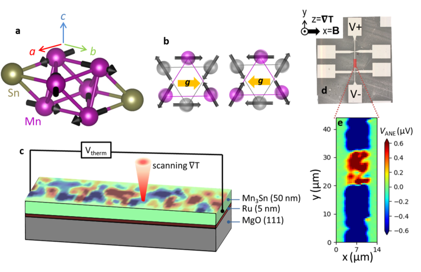
As demonstrated by Ikhlas et al. Ikhlas et al. (2017), the anomalous Nernst response of MnSn is strongly anisotropic. No anomalous Nernst voltage is expected when the thermal gradient is applied in the -plane Ikhlas et al. (2017), while in the direction perpendicular to the g vector is expected when is applied along the -axis. In our sample, laser generated heat drains into the substrate, the in-plane components (in -plane) compensate each other and the remaining thermal gradient is along the direction (-axis). Magnetic field is applied along the direction and we detect along the direction. Thus, the thermo-voltage signal is determined by the projection of the g vector onto the direction. The different magnitude and sign of observed depending on the position of the laser spot on the sample thus reflects the corresponding local orientation of the vector g in the irradiated area. Note that the laser beam is focused to a diameter of 1.5 m, such that reflects the average of possibly different g orientations or domains present within the illuminated spot. The measured voltage is therefore proportional to the net (average) component of the g vectors perpendicular to the detection direction. The resolution of the STGM is discussed in more detail in the SI. Remarkably, we observe very different patterns depending on the sample history. As discussed below, magnetic domains can be intentionally written into the MnSn using local heating. The domain pattern shown in Fig. 1e is the result of such a process. On the other hand, upon cooling the sample from in zero magnetic field, domains are randomly populated resulting in more complex magnetic spatial contrast, as can be seen for example in Fig. 2a,b. Several Hall bars with different orientation with respect to the [100] direction of MnSn were measured showing similar results.
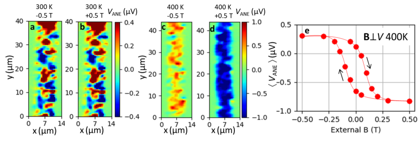
We now demonstrate that the signal is indeed of magnetic origin, and that it can be reversed by an external magnetic field. It is important to note that the magnetic field required for the reversal of spins in MnSn thin films is higher compared to bulk MnSn crystals You et al. (2019); Higo et al. (2018b). Therefore, in our thin film samples, the spin structure cannot be reversed by 0.5 T (the experimentally available field) at temperatures below 300 K, as can be seen in Fig. 2a,b. At 375 K a small variation of the measured signal depending on the polarity of the magnetic field can be seen (SI Fig. 5) corresponding to a reorientation of domains with the weakest coercivity. In contrast, increasing the sample temperature to 400 K and then applying a magnetic field allows us to completely alter the domain pattern, as shown in Fig. 2c,d. At 400 K, the majority of domains is following the external magnetic field. A magnetic field of yields a positive STGM map (red color) across the entire region scanned with the laser spot (Fig. 2c), while for +, the STGM map turns negative (blue color) (Fig. 2d). This shows that at , which is close to the Néel temperature , a magnetic field of suffices to align the g vector along the field direction in the entire sample. At the same time the net magnetic moment detected by SQUID magnetometry (see SI, Fig. 2) remains unchanged between 300 K and 400 K, such that ferromagnet-like phases appearing at higher temperatures can be excluded. To further study the impact of the magnetic field on the magnetic domain pattern, we recorded STGM maps for several different magnetic field values in a “field sweep”. As detailed in the SI, a complex reversal behavior with multiple domains is observed (for individual maps at each magnetic field see SI Fig. 4). In Fig. 2e, we plot the voltage averaged over the whole scanned area as a function of the field strength, and find a global magnetic hysteresis curve with a clear saturation, coercivity and remanence. Since we observe a sign reversal in as a function of the magnetic field, the signal is odd under spin reversal and therefore the main contribution has the Nernst symmetry. The magneto-thermo-voltage clearly cannot be explained by an ordinary Nernst effect, which is linear in magnetic field and does not show hysteresis. Instead, the observed must be connected to the magnetic order parameter of the antiferromagnet. Moreover, when applying the magnetic field parallel to the voltage detection direction, shows no remanence or saturation at (SI Fig. 3). This supports the notion that the component of g perpendicular to the voltage detection determines .
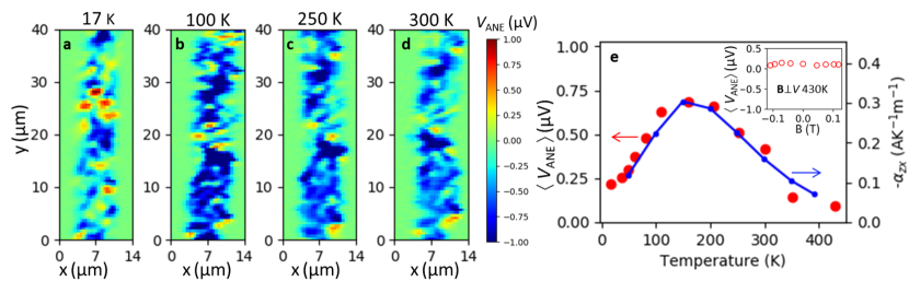
An additional confirmation that the spatial contrast of STGM maps is governed by the antiferromagnetic order in MnSn is evident from the evolution of the STGM signal with temperature. Figure 3 shows scans taken at different in the range of to . The sample was first cooled to in zero magnetic field and then warmed up step by step to higher temperatures. No magnetic field was applied during this experiment, such that also data at 400 K exhibit a lower voltage compared to the polarized state (Fig. 2). We find a subtle but robust variation with . The net amplitude plotted in Fig. 3e peaks in the vicinity of , in excellent agreement with the temperature dependence of the anomalous Nernst response reported in bulk MnSn crystals Ikhlas et al. (2017) which is reproduced in Fig. 3e (blue line). Above , the thermo-voltage signal vanishes. Indeed, the magnetic field dependent experiments performed at , depicted in the inset of Fig. 3e, show that is zero, with no signs of remanence or saturation. Note that we did not detect any evidence for a spin glass phase in our samples below 50 K Nakatsuji et al. (2015). Here again, the different magnetic anisotropy of thin films might affect the presence of the spin glass phase Ritchey et al. (1993); Bisson and Wills (2008).
The STGM does not allow for a direct evaluation of the anomalous Nernst coefficient. The reason is that, unlike in the case of a conventional in-plane thermal gradient, the magnitude of cannot be directly measured since no thermometry “below the film” is possible. The laser induced thermal gradient can, however, be estimated by comparing to a film with a known magneto-thermal coefficient deposited on a similar substrate. For the present study, we use a thin film of the Weyl semimetal Co2MnGa Reichlova et al. (2018). We obtain a thermal gradient of 2 Km for a laser power of 10 mW, as detailed in the SI, resulting in an anomalous Nernst coefficient of 1.5-2 V/K for the MnSn thin film at room temperature. This is higher than the value reported in bulk MnSn crystals 0.6 V/K Ikhlas et al. (2017), which could be due to the higher degree of domain polarization or the more localized detection in our thin film sample. Since the estimation of the thermal gradient contains significant error bars, a more systematic study of the Nernst effect magnitude in thin films is an important future task.
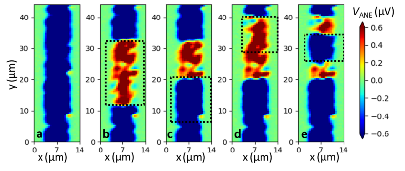
The capability to intentionally write magnetic domains is exceptionally important not only from an application perspective Parkin et al. (2008), but also to quantify spin transfer torque DuttaGupta et al. (2015), domain wall motion or giant magnetoresistance Gregg et al. (1996) in antiferromagnets. In Fig. 4, we show that magnetic domains can be intentionally written into the MnSn film at room temperature, via a combination of high-power () laser illumination and external magnetic fields. Hereby, it is of key importance that the external magnetic field does not alter the magnetic texture in MnSn at room temperature in the absence of the laser heating (see Fig. 2a,b).
Fig. 4 shows a sequence of writing and erasing of domains at 300 K using the following procedure: First, the full area (region of interest) is scanned with a laser spot in + external field applied along direction. Subsequently, the same area is investigated using STGM with laser power (Fig. 4a), showing a homogeneous thermo-voltage contrast and, thus, homogeneous g vector orientation. In the next step, only the area enclosed by the dashed line is scanned with , now with applied , followed by imaging the entire area with STGM with laser power (Fig. 4b). Repeated STGM maps with either , or have no impact on the written pattern (SI Fig. 8), even a magnetic field of 6 T applied along direction at 300 K could not erase the domain pattern (SI).
However, increasing the laser power up to again allows us to write domain patterns at will (Fig. 4c-e). In particular, re-writing the same area with the same magnetic field polarity does not alter the contrast, while writing with opposite field polarity invariably reverses the sign of the thermo-voltage.
Our work demonstrates that the magnetic structure in the non-collinear antiferromagnet MnSn can be spatially mapped out using local laser heating in combination with anomalous Nernst effect measurements. At room temperature and below, the magnetic structure is insensitive to magnetic fields up to 6 T. We further show that domains can be intentionally written into the magnetic structure, via the application of local heat in combination with moderate magnetic fields (). Our experiments, thus, open a pathway to initializing and detecting a domain pattern in non-collinear antiferromagnetic thin films. This represents a first important step towards studying the intriguing physics of non-collinear AFMs with spatial resolution, such as spin transfer torque-induced domain wall motion or spin flop mechanisms in triangular spin systems. Our technique can be straightforwardly extended to a range of materials, given that they exhibit a finite magneto-thermal response (ANE, anisotropic magneto-thermo power etc.) and, therefore, represents a versatile tool for the investigation of local magnetic properties.
Methods: Growth MnSn films were grown by a BesTec UHV magnetron sputtering system on MgO (111) substrates with a 5 nm Ru underlayer. Prior to deposition, the chamber was evacuated to a base pressure of less than 5 10-9 mbar, while the process gas (Ar 5 N) pressure was 3 10-3 mbar. The Ru underlayer was deposited at a rate of 0.45 Å/s by applying 30 W dc power to a 2 inch target. The MnSn films were grown by cosputtering. The Mn was deposited at a rate of 0.49 Å/s by applying 42 W dc power and the Sn at a rate of 0.30 Å/s by applying 11 W dc power to a 3 and 2 inch target, respectively. The growth rates and the film thicknesses were determined by a quartz crystal microbalance and confirmed by using x-ray reflectivity measurements. The substrates were rotated during deposition, to ensure homogeneous growth. The Ru underlayer was grown at 400∘ C, the MnSn at RT and finally the stack was post-annealed at 300∘ C in-situ for 10 mins. All films were capped with 3 nm of Al to prevent oxidation. Experimental Setup The thermal gradient is generated by a continuous wave laser operating at a wavelength of =800 nm and focused by an objective lens to a spot size of 1.5 m (see Fig.1c). The laser power can be continuously tuned by a combination of a half-wave plate and a polarizer. Scanning of the laser spot across the Hall bar is accomplished by moving the objective lens with a 3D piezo-positioner and the thermo-voltage generated along the direction is recorded in each position. The laser beam is modulated by a chopper at frequency of 1.7 kHz and the generated thermo-voltage is detected using a lock-in amplifier.
We acknowledge Jakob Lindermeir for technical support, IFW Dresden for providing access to the MST lab, EU FET Open RIA Grant no. 766566, support from the Grant Agency of the Czech Republic under EXPRO grant no. 19-28375X, and financial support from the DPG through project B05 and C08 of SFB 1143 (project-id 247310070).
References
- Jungwirth et al. (2018) T. Jungwirth, J. Sinova, A. Manchon, X. Marti, J. Wunderlich, and C. Felser, Nature Physics 14, 200 (2018).
- Baltz et al. (2018) V. Baltz, A. Manchon, M. Tsoi, T. Moriyama, T. Ono, and Y. Tserkovnyak, Reviews of Modern Physics 90, 015005 (2018).
- Suergers et al. (2014) C. Suergers, G. Fischer, P. Winkel, and H. v. Löhneysen, Nature Communications 5, 3400 (2014).
- Zhang et al. (2014) W. Zhang, M. B. Jungfleisch, W. Jiang, J. E. Pearson, A. Hoffmann, F. Freimuth, and Y. Mokrousov, Physical Review Letters 113, 196602 (2014).
- Nakatsuji et al. (2015) S. Nakatsuji, N. Kiyohara, and T. Higo, Nature 527, 212 (2015).
- Nayak et al. (2016) A. K. Nayak, J. E. Fischer, Y. Sun, B. Yan, J. Karel, A. C. Komarek, C. Shekhar, N. Kumar, W. Schnelle, J. Kuebler, C. Felser, and S. S. P. Parkin, Science Advances 2, e1501870 (2016).
- Ikhlas et al. (2017) M. Ikhlas, T. Tomita, T. Koretsune, M.-T. Suzuki, D. Nishio-Hamane, R. Arita, Y. Otani, and S. Nakatsuji, Nature Physics 13, 1085 (2017).
- Higo et al. (2018a) T. Higo, H. Man, D. B. Gopman, L. Wu, T. Koretsune, O. M. J. van ’t Erve, Y. P. Kabanov, D. Rees, Y. Li, M.-T. Suzuki, S. Patankar, M. Ikhlas, C. L. Chien, R. Arita, R. D. Shull, J. Orenstein, and S. Nakatsuji, Nature Photonics 12, 73 (2018a).
- Kimata et al. (2019) M. Kimata, H. Chen, K. Kondou, S. Sugimoto, P. K. Muduli, M. Ikhlas, Y. Omori, T. Tomita, A. H. MacDonald, S. Nakatsuji, and Y. Otani, Nature 566, E4 (2019).
- Kuroda et al. (2017) K. Kuroda, T. Tomita, M.-T. Suzuki, C. Bareille, A. A. Nugroho, P. Goswami, M. Ochi, M. Ikhlas, M. Nakayama, S. Akebi, R. Noguchi, R. Ishii, N. Inami, K. Ono, H. Kumigashira, A. Varykhalov, T. Muro, T. Koretsune, R. Arita, S. Shin, T. Kondo, and S. Nakatsuji, Nature Materials 16, 1090 (2017).
- Železný et al. (2017) J. Železný, Y. Zhang, C. Felser, and B. Yan, Physical Review Letters 119, 187204 (2017).
- Weiler et al. (2012) M. Weiler, M. Althammer, F. D. Czeschka, H. Huebl, M. S. Wagner, M. Opel, I.-M. Imort, G. Reiss, A. Thomas, R. Gross, and S. T. B. Goennenwein, Physical Review Letters 108, 106602 (2012).
- Kuebler and Felser (2014) J. Kuebler and C. Felser, EPL (Europhysics Letters) 108, 67001 (2014).
- Yang et al. (2017) H. Yang, Y. Sun, Y. Zhang, W.-J. Shi, S. S. P. Parkin, and B. Yan, New Journal of Physics 19, 015008 (2017).
- Liu and Balents (2017) J. Liu and L. Balents, Physical Review Letters 119, 087202 (2017).
- Manna et al. (2018) K. Manna, Y. Sun, L. Muechler, J. Kübler, and C. Felser, Nature Reviews Materials 3, 244 (2018).
- Tomiyoshi and Yamaguchi (1982) S. Tomiyoshi and Y. Yamaguchi, Journal of the Physical Society of Japan 51, 2478 (1982).
- Sticht et al. (1989) J. Sticht, K.-H. Hoeck, and J. Kuebler, Journal of Physics: Condensed Matter 1, 8155 (1989).
- Brown et al. (1990) P. J. Brown, V. Nunez, F. Tasset, J. B. Forsyth, and P. Radhakrishna, Journal of Physics: Condensed Matter 2, 9409 (1990).
- Zhang et al. (2013) D. Zhang, B. Yan, S.-C. Wu, J. Kübler, G. Kreiner, S. S. P. Parkin, and C. Felser, Journal of Physics: Condensed Matter 25, 206006 (2013).
- Sung et al. (2018) N. H. Sung, F. Ronning, J. D. Thompson, and E. D. Bauer, Applied Physics Letters 112, 132406 (2018).
- Kleiner (1966) W. H. Kleiner, Physical Review 142, 318 (1966).
- Smejkal et al. (2019) L. Smejkal, R. Rafael González-Hernández, T. Jungwirth, and J. Sinova, “arxiv:1901.00445,” (2019).
- Guo and Wang (2017) G.-Y. Guo and T.-C. Wang, Physical Review B 96, 224415 (2017).
- Markou et al. (2018) A. Markou, J. M. Taylor, A. Kalache, P. Werner, S. S. P. Parkin, and C. Felser, Physical Review Materials 2, 051001 (2018).
- You et al. (2019) Y. You, X. Chen, X. Zhou, Y. Gu, R. Zhang, F. Pan, and C. Song, Advanced Electronic Materials , 1800818 (2019).
- Higo et al. (2018b) T. Higo, D. Qu, Y. Li, C. L. Chien, Y. Otani, and S. Nakatsuji, Applied Physics Letters 113, 202402 (2018b).
- Ritchey et al. (1993) I. Ritchey, P. Chandra, and P. Coleman, Physical Review B 47, 15342 (1993).
- Bisson and Wills (2008) W. G. Bisson and A. S. Wills, Journal of Physics: Condensed Matter 20, 452204 (2008).
- Reichlova et al. (2018) H. Reichlova, R. Schlitz, S. Beckert, P. Swekis, A. Markou, Y.-C. Chen, D. Kriegner, S. Fabretti, G. H. Park, A. Niemann, S. Sudheendra, A. Thomas, K. Nielsch, C. Felser, and S. T. B. Goennenwein, Applied Physics Letters 113, 212405 (2018).
- Parkin et al. (2008) S. S. P. Parkin, M. Hayashi, and L. Thomas, Science 320, 190 (2008).
- DuttaGupta et al. (2015) S. DuttaGupta, S. Fukami, C. Zhang, H. Sato, M. Yamanouchi, F. Matsukura, and H. Ohno, Nature Physics 12, 333 (2015).
- Gregg et al. (1996) J. F. Gregg, W. Allen, K. Ounadjela, M. Viret, M. Hehn, S. M. Thompson, and J. M. D. Coey, Physical Review Letters 77, 1580 (1996).