Imaging of current induced Néel vector switching in antiferromagnetic Mn2Au
Abstract
The effects of current induced Néel spin-orbit torques on the antiferromagnetic domain structure of epitaxial Mn2Au thin films were investigated by X-ray magnetic linear dichroism - photoemission electron microscopy (XMLD-PEEM). We observed current induced switching of AFM domains essentially corresponding to morphological features of the samples. Reversible as well as irreversible Néel vector reorientation was obtained in different parts of the samples and the switching of up to 30 % of all domains in the field of view of 10 m is demonstrated. Our direct microscopical observations are compared to and fully consistent with anisotropic magnetoresistance effects previously attributed to current induced Néel vector switching in Mn2Au.
pacs:
In antiferromagnetic (AFM) spintronics the staggered magnetization, or more precisely the Néel vector describing the spin structure, can be used to encode information Jun18 ; Bal18 ; Jung18 . For the switching of the Néel vector and the read-out of its orientation different strategies have been pursued Son18 . The Néel vector was e. g. manipulated by an exchange-spring effect with a ferromagnet (FM) and read-out via tunneling anisotropic magnetoresistance (T-AMR) measurements Par11 ; Fin14 . Other experiments were based on a ferromagnet to AFM phase transition Mar14 or on strain induced anisotropy modifications Sap17 . However, for antiferromagnetic spintronics Néel vector switching by current-induced spin-orbit torques (SOTs) Zel18 , whose FM counterparts are already established for memory applications Gam11 ; Bra14 , are most promising due to superior scaling, switching speed and device compatibility.
The SOTs used for FM spintronics are typically generated at interfaces with heavy metals Mir11 ; Liu12 . However, a specific crystallographic structure with oppositely broken inversion symmetry on the each of the collinear AFM sublattices makes Mn2Au and CuMnAs up to now the only known antiferromagnets, for which a so called bulk Néel spin-orbit torque (NSOT) Zel14 can enable current induced Néel vector manipulation in a single layer system. Indeed, this was demonstrated experimentally for CuMnAs Wad16 ; Wad18 and, more recently, for Mn2Au Bod18 ; Zho18 ; Mei18 as well.
Whereas in the case of CuMnAs, the modification of the AFM domain structure by current pulses was observed directly by X-ray magnetic linear dichroism - photoelemission electron microscopy (XMLD-PEEM) Wad18 ; Grz17 , such microscopic insights are missing for Mn2Au up to now. However, direct imaging of the effect of current pulses on the Néel vector orientation is crucial for the interpretation of previously published results of resistivity changes attributed to a Néel vector reorientation in Mn2Au Bod18 ; Zho18 ; Mei18 . Furthermore, magnetic microscopy enables the identification of important quantities and mechanisms of the Néel vector manipulation such as switched volume fraction, morphological influence on the domain pattern, and domain wall motion.
In this paper we demonstrate the imaging of current induced modifications of the AFM domain structure of epitaxial Mn2Au thin films and relate the results to previous transport measurements.
We investigated epitaxial Mn2Au(001) thin films deposited by RF sputtering from a single stoichiometric target directly onto heated Al2O3 substrates. Although there is no obvious epitaxial relation of Mn2Au with this substrate, the thin films grow in comparable quality including in-plane order as we reported previously for Mn2Au(001) grown on a Ta(001) buffer layer on the same type of substrate Jou15 . All samples have a thickness of 80 nm and were capped in-situ by nm of Al as a protection against oxidation. The thin films were then patterned by optical lithography and ion beam etching into a cross structure with a central area of to enable current pulsing analogous to our previous experiments, i. e. with current densities of A/cm2 and a pulse durations of 1 ms Bod18 .
The XMLD-PEEM imaging was performed at beamline I06 at Diamond Light Source in the same way as for our previous investigation of the AFM domain pattern of 240 nm thick Mn2Au(001) thin films modified by spin-flop in large external magnetic fields Sap18 . In this set-up the sample is illuminated under a grazing incidence angle of by X-rays linearly polarized in the sample plane. Due to the grazing angle of incidence, the XMLD contrast can barely be generated by a rotation of the polarization direction. Instead, two PEEM images were taken with X-ray energies corresponding to the maximum and the minimum of the XMLD as determined in Sap17 . roughly corresponds to the absorption maximum of Mn, whereas sits on the low energy side of the edge. However, an asymmetry XMLD-PEEM contrast given by
| (1) |
always shows additional to the magnetic contrast generated by the XMLD effect morphological contrast originating from the subtraction two morphology containing images obtained on and off the edge.
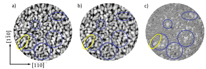
Our Mn2Au samples with a thickness of 80 nm used for current induced Néel vector switching show many more morphological features in PEEM than the 240 nm thick films used in Sap18 . Fig. 1 a) shows an asymmetry image of such a sample in the as grown state with the direction of X-ray incidence selected such that magnetic contrast appears for a Néel vector alignment parallel to the easy [110]- and [10] directions Sap18 ; Shi10 .
Different brightness levels of the morphological grains indicate AFM domains, but the magnetic contrast is much weaker than the morphological contribution. Correspondingly, upon rotation of a sample by 90o as in Sap18 we observed only small changes of the XMLD-PEEM images generated by the contrast inversion due to XMLD. However, considering current induced changes of the Néel vector of the samples, the subtraction of asymmetry XMLD-PEEM images obtained before and after the modification of the magnetic state removes the morphological contrast and results in a difference image clearly showing all modified AFM domains as described below.
We then applied 100 current pulses with an amplitude of A/cm2 and a length of 1 ms (with a delay of 10 ms between each single pulse) parallel to the [110]-direction and afterward obtained the asymmetry image shown in Fig. 1 b). It is now possible to observe relative changes of brightness of several morphological grains with respect to the brightness of the surrounding area. The most obvious positions of such changes are indicated by blue circles within the images in Fig. 1. This is the effect of a Néel vector reorientation of these grains, which is already visible upon closer inspection of the asymmetry images 1 a) and 1 b). Fig. 1 c) shows the difference of these images, thereby removing the morphological contrast. Switched grains now appear bright on a homogeneous background. Blue circles at the same position as in 1 a) and 1 b) serve to guide the eye. It is obvious that the applied train of current pulses mostly switched the Néel vector of complete morphological grains, which indicates that typically the AFM domains correspond to morphological grains and are for these samples of a typical size of nm. However, in the region indicated by the yellow circles in Fig. 1 also a partial switching of a grain is observed.
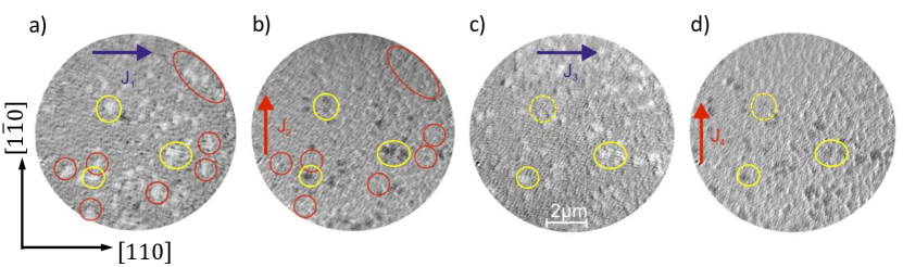
Next we study the effects of subsequently applied current pulses along two perpendicular easy directions on the AFM domain structure. After the first set of current pulses already discussed above, a second set of pulses was applied in the perpendicular easy-axis direction, i. e. along [10] and another XMLD-PEEM asymmetry image was acquired. This procedure was repeated twice always using the same pulse current densities. The corresponding difference images are shown in Fig. 2 a)-d) with the direction of the current indicated. From these images it is obvious that some of the morphological grains/ AFM domains switch reversibly. Examples are indicated by the yellow circles in Fig. 2. However, other grains, indicated by the red circles, switch irreversibly. This could be explained by local strain induced variations of the magnetocrystalline anisotropy. Alternatively, also an inhomogeneous current density could result in locally irreversible switching behavior. Considering the large AMR effect of several percent associated with the rotation of the Néel vector Bod18 , each switching event of a domain results in a redistribution of the inhomogeneous current density, could generate locally irreversible switching behavior.
For a quantitative analysis of the switched fraction of the AFM domains we evaluated the area of the switched domains in the difference images (Fig. 3, black squares).
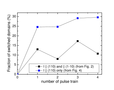
To obtain the switched fraction the gray scale difference images were converted into black and white images adjusting the threshold in a way that the as determined by eye best correspondence of the switched areas was obtained. The final quantification was obtained from histograms of these binary images.
Fig. 3 shows a higher switching probability for the horizontal (pulse trains no. 1 and 3) than for the vertical (pulse trains no. 2 and 4) current directions. This is consistent with our observation of a trend toward slightly larger/ smaller resistances when switching the magnetoresistance of Mn2Au by subsequent current pulses in perpendicular directions Bod18 . The associated breaking of symmetry can be explained by a tilt of the crystallographic (001)-axis with respect to the substrate normal of about 2o as identified by X-ray diffraction, which could affect e. g. the magnetocrystalline anisotropy.
Next we study the influence of the number of current pulses and of the pulse current density on the resulting fraction of switched AFM domains. For this we investigated a Mn2Au thin film with a prealigned Néel vector, i. e. we started from a well defined magnetic configuration with the Néel vector aligned parallel [10]. This was achieved by exposing the sample to a 60 T external magnetic field pulse (60 ms) at the Helmholtz-Zentrum Dresden-Rossendorf as described in Sap18 prior to the XMLD-PEEM beam time.
For current densities A/cm2 no Néel vector reorientations were observed. The first set of 100 current pulses with a current density of A/cm2 along [10] switched already a large fraction of the AFM domains as shown in the difference image obtained from two XMLD-PEEM images acquired before and after the current pulses (Fig. 4 a).
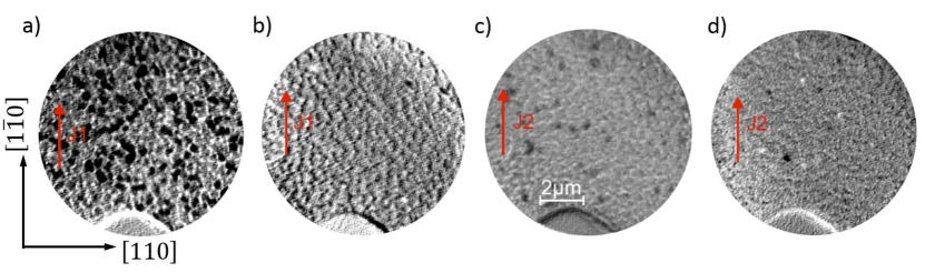
Additional 100 pulses with the same current density along the same direction reoriented almost no further domains (Fig. 4 b). However, another 100 current pulses with an increased current density of A/cm2 again switched a significant amount of additional domains (Fig. 4 c). This was again possible (to a smaller extend) by the application of a second set of pulses with the same current density (Fig. 4 d). At the attempt to continue this procedure with a current density of A/cm2 the sample suffered from electrical breakdown.
Again we quantify the switched fraction of the domains by analyzing the areas of the dark spots in Figs. 4 a-d). The result is shown in Fig. 3 (blue squares) and indicates that the first set of 100 current pulses switched about 25 % of all domains. After all subsequent applications of current pulse trains the total amount of switched domains increased to % before this sample was destroyed.
This relatively large fraction of reoriented domains is consistent with the large resistivity change associated with the current induced Néel vector manipulation, which we observed previously Bod18 . Although we could not demonstrate complete switching of all domains, our results together with our previous transport experiments suggest that this can be realized in Mn2Au. Investigating more samples and increasing the pulse current density more carefully, presumably larger switched fractions could be demonstrated. However, this was not possible due to time limitations of beamtime.
In conclusion, we visualized AFM domain patterns of Mn2Au samples, which are reflecting the morphology of these thin films with a typical domain/ grain size of nm. The application of current pulses with a typical current density of A/cm2 resulted mainly in rotations of the Néel vector of domains corresponding to morphological grains. These grains switch partially reversibly and partially irreversibly, which could be explained by local variations of the magnetocrystalline anisotropy or by an inhomogeneous current redistribution. Current induced modifications of the domain pattern were observed exactly within the small window of switching current densities in which we previously observed relatively large resistance changes of the Mn2Au thin films Bod18 . This represents an important confirmation that our previous assumption of a large AMR effect associated with a reorientation of the Néel vector in Mn2Au is correct. The fraction of switchable domains increases with increasing current density until destruction of the sample due to current overload. We visualized a maximum switching of % of all domains in the central area of a patterned cross structure with 10 m width, representing a significant fraction of the area previously probed by transport experiments Bod18 .
References
- (1) T. Jungwirth, J. Sinova, A. Manchon, X. Marti, J. Wunderlich, C. Felser, Nat. Phys. 14, 200 (2018).
- (2) V. Baltz, A. Manchon, M. Tsoi, T. Moriyama, T. Ono, and Y. Tserkovnyak, Rev. Mod. Phys. 90, 015005 (2018).
- (3) M. B. Jungfleisch, W. Zhang, A. Hoffmann, Phys. Lett. A 382, 865 (2018).
- (4) C. Song, Y. You, X. Chen, X. Zhou, Y. Wang and F. Pan, Nanotechnology 29, 112001 (2018)
- (5) B. G. Park, J. Wunderlich, X. Marti, V. Holý, Y. Kurosaki, M. Yamada, H. Yamamoto, A. Nishide, J. Hayakawa, H. Takahashi, A. B. Shick, T. Jungwirth, Nat. Mater. 10, 347 (2011).
- (6) I. Fina, X. Marti, D. Yi, J. Liu, J. H. Chu, C. Rayan-Serrao, S. Suresha, A. B. Shick, J. Železný, T. Jungwirth, J. Fontcuberta, and R. Ramesh, Nat. Commun. 5, 4671 (2014).
- (7) X. Marti, I. Fina, C. Frontera, Jian Liu, P. Wadley, Q. He, R. J. Paull, J. D. Clarkson, J. Kudrnovský, I. Turek, J. Kunes, D. Yi, J-H. Chu, C. T. Nelson, L. You, E. Arenholz, S. Salahuddin, J. Fontcuberta, T. Jungwirth, and R. Ramesh et al., Nat. Mater. 13, 367 (2014).
- (8) A. A. Sapozhnik, R. Abrudan, Yu. Skourski, M. Jourdan, H. Zabel, M. Kläui, and H.-J. Elmers, Phys. Status Solidi, 4, 1600438 (2017).
- (9) J. Železný, P. Wadley, K. Oljenik, A. Hoffmann, H. Ohno, Nat. Phys. 14, 220 (2018).
- (10) P. Gambardella and I. M. Miron, Philos. Trans.,R. Soc. A 369, 3175 (2011).
- (11) A. Brataas and K.M.D. Hals, Nat. Nanotech. 9, 86 (2014).
- (12) I. Miron, K. Garello, G. Gaudin, P. J. Zermatten, M. V. Costache, S. Auffret, S. Bandiera, B. Rodmacq, A. Schuhl, P. Gambardella, Nature 476, 189 (2011).
- (13) L. Liu, C.F. Pai, Y. Li, H. W. Tseng, D. C. Ralph, R. A. Buhrman, Science 336, 555 (2012).
- (14) J. Železný H. Gao, K. Výborný, J. Zemen, J. Masek, A. Manchon, J. Wunderlich, J. Sinova, and T. Jungwirth., Phys. Rev. Lett. 113, 157201 (2014).
- (15) P. Wadley B. Howells, J. Železn’y, C. Andrews, V. Hills, R. P. Campion, V. Novák, K. Olejnik, F. Maccherozzi, S. S. Dhesi, S. Y. Martin, T. Wagner, J. Wunderlich, F. Freimuth, Y. Mokrousov, J. Kunes, J. S. Chauhan, M. J. Grzybowski, A. W. Rushforth, K. W. Edmonds, B. L. Gallagher, T. Jungwirth, Science 351, 587 (2016).
- (16) P. Wadley, S. Reimers, M. J. Grzybowski, C. Andrews, M. Wang, J. S. Chauhan, B. L. Gallagher, R.¶. Campion, K. W. Edmonds, S. S. Dhesi, F. Maccherozzi, V. Novak, J. Wunderlich, and T. Jungwirth , Nat. Nanotech. 13, 632 (2018).
- (17) S. Bodnar L. Smejkal, I. Turek, T. Jungwirth, O. Gomonay, J. Sinova, A.A. Sapozhnik, H.-J. Elmers, M. Kläui, and M. Jourdan, Nat. Commun. 9, 348 (2018).
- (18) X. F. Zhou, J. Zhang, F. Li, X. Z. Chen, G. Y. Shi, Y. Z. Tan, Y. D. Gu, M. S. Saleem, H. Q. Wu, F. Pan, and C. Song, Phys. Rev. Appl. 9, 054028 (2018).
- (19) M. Meinert, D. Graulich, and T. Matalla-Wagner, Phys. Rev. Appl. 9 , 064040 (2018).
- (20) M. Grzybowski, P. Wadley, K. Edmonds, R. Beardsley, V. Hills, R. Campion, B. Gallagher, J. Chauhan, V. Novak, T. Jungwirth, F. Maccherozzi, and S. Dhesi, Phys. Rev. Lett. 118, 057701 (2017).
- (21) M. Jourdan, H. Bräuning, A. Sapozhnik, H.-J. Elmers, H. Zabel and M. Kläui, J. Phys. D: Appl. Phys. 48, 385001 (2015).
- (22) A. A. Sapozhnik M. Filianina, S. Yu. Bodnar, A. Lamirand, M.-A. Mawass, Y. Skourski, H.-J. Elmers, H. Zabel, M. Kläui, and M. Jourdan, Phys. Rev. B 97, 134429 (2018).
- (23) A. B. Shick, S. Khmelevkyi, O. N. Mryasov, J. Wunderlich, and T. Jungwirth, Phys. Rev. B 81, 212409 (2010).
Acknowledgements
This work is supported by the German Research Foundation (DFG) through the Transregional Collaborative Research Center SFB/TRR173 Spin+X, Projects A03 and A05. We thank the Diamond Light Source for the allocation of beam time under Proposal No. SI20534-1. We acknowledge the support of the HLD at HZDR, member of the European Magnetic Field Laboratory (EMFL), and by EPSRC (U.K.) via its membership to the EMFL (Grants No. EP/N01085X/1 and No. NS/A000060/1).