Mitigation of Cosmic Ray Effect on Microwave Kinetic Inductance Detector Arrays
Abstract
For space observatories, the glitches caused by high energy phonons created by the interaction of cosmic ray particles with the detector substrate lead to dead time during observation. Mitigating the impact of cosmic rays is therefore an important requirement for detectors to be used in future space missions. In order to investigate possible solutions, we carry out a systematic study by testing four large arrays of Microwave Kinetic Inductance Detectors (MKIDs), each consisting of 960 pixels and fabricated on monolithic 55 mm 55 mm 0.35 mm Si substrates. We compare the response to cosmic ray interactions in our laboratory for different detector arrays: A standard array with only the MKID array as reference; an array with a low superconducting film as phonon absorber on the opposite side of the substrate; and arrays with MKIDs on membranes. The idea is that the low layer down-converts the phonon energy to values below the pair breaking threshold of the MKIDs, and the membranes isolate the sensitive part of the MKIDs from phonons created in the substrate. We find that the dead time can be reduced up to a factor of 40 when compared to the reference array. Simulations show that the dead time can be reduced to below 1 % for the tested detector arrays when operated in a spacecraft in an L2 or a similar far-Earth orbit. The technique described here is also applicable and important for large superconducting qubit arrays for future quantum computers.
pacs:
Valid PACS appear hereData loss caused by cosmic ray hits on the instruments’ detectors is one of the main concerns for space observatories. Cosmic rays are so energetic that they penetrate the satellite structure, reach the detectors, and deposit a fraction of their energy through ionization and atomic excitation. The deposited energy causes a cascade of high-energy phonons (ballistic phonons) that spread inside the detectors, trigger the detectors’ response, and create glitches in the data stream. These glitches lead to significant dead time of the detectors and loss of integration efficiency Planck Collaboration (2014). Although cosmic ray interactions are strongest in space, even on earth the interaction rate is about a few events/min/cm2, posing possible issues especially for cryogenic superconducting circuits with large areas, such as quantum computing chips.
Microwave Kinetic Inductance Detectors (MKIDs) Day et al. (2003); Zmuidzinas (2012) are pair breaking detectors that sense a change in Cooper pair density due to radiation absorption, in contrast to bolometric detectors, such as Transition Edge Sensors Irwin (1995), which measure temperature. Hence, MKIDs only sense energies larger than the gap energy of a superconductor film (). In the Planck satellite, in which bolometers are used, short and long glitches are observed due to cosmic rays Catalano et al. (2014). Short glitches, with a decay of 4-10 ms, are determined to be direct hits in the bolometer. Long glitches, with a time scale exceeding 10 ms, are interpreted as cosmic ray hits in the Si wafer. The measurements of cosmic ray interactions on arrays of MKIDs on earth show interactions with two time scales: the ballistic phonon thermalization time, which is in the order of 0.1 ms Catalano et al. (2016), and the quasiparticle recombination time (). The latter depends on the background loading on the detector and varies between 0.01 ms for the high power background of a ground based imaging system to values in excess of 1 ms for low background applications in space de Visser et al. (2014). The dead time fraction caused by cosmic rays is therefore expected to be smaller in case of MKIDs.
Adding a superconducting layer with a critical temperature () below or close to the of the material of the MKID is an idea to further harden MKID arrays against the effects of cosmic ray hits by reducing the phonon energy Monfardini et al. (2016). In the low layer, the energies of high energy ballistic phonons are converted by electron-phonon interaction into phonons with energies mostly in between 2 to Kozorezov et al. (2000); Goldie and Withington (2013). Phonons emitted due to scattering will have even lower energy than . Thus if the of the additional layer is chosen , most of the cosmic ray energy will be quickly converted into low energy phonons to which the MKID is not sensitive. Making the detector on a membrane structure is another idea to harden the MKID array for cosmic ray interactions by suppressing the propagation of high energy phonons towards the detector Holmes et al. (2008).
In this letter, we measure the dead time due to cosmic ray interactions in four types of NbTiN-Al hybrid MKID arrays Janssen et al. (2013); Baselmans et al. (2017).
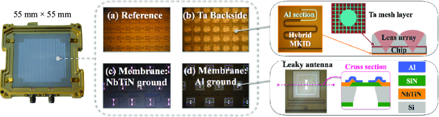
All arrays are made on a 55 mm 55 mm 0.35 mm chip and contain about 960 hybrid MKIDs Janssen et al. (2013), fabricated from NbTiN with a K, in which a small Al section of about 1.2 mm long ( K) is used as the radiation detection area. It needs to be mentioned that we sense only pair breaking events in this aluminium; pair breaking and subsequent recombination in the NbTiN area of the detector is much faster than the detector time constant and is thereby efficiently filtered. Figure 1 displays the 4 configurations of measured chips:
-
()
A reference array with the NbTiN-Al MKIDs fabricated on a solid sapphire substrate without any backside layer or membrane structure Janssen et al. (2013).
- ()
-
()
An array with the Al section of the MKID on a membrane of 1 m thick SiN (ground of the resonator is NbTiN). Each MKID is coupled to a leaky lens antenna Hähnle et al. .
- ()


We evaluate the effect of cosmic ray interactions in the detector chips by measuring the effects of secondary cosmic rays in the laboratory. The chips are placed horizontally in a dark, cold (120 mK) environment using an Adiabatic Demagnetization Refrigerator (ADR) with a box-in-box light-tight setup Baselmans et al. (2012), 111Chip and has a gold layer at edges to have a good thermal contact to the gold-plated sample box. The layer is intended to better thermalize the chip under sub-mm illumination Yates et al. (2017).. In order to accumulate statistics, we took 30 minutes () of time ordered data for each chip with a multiplexing readout system van Rantwijk et al. (2016) with a sampling rate of kHz (s). We can resolve the shape of the glitches with this sampling speed and evaluate by fitting the glitch tails with a single exponential function Baselmans et al. (2017). Considering the typical muon rate of a few events/min/cm2 at the ground, we expect about a few thousands cosmic ray events observed in each chip. The main component of secondary cosmic rays is muons that result from the interaction of primary cosmic rays (mainly protons) with the Earth’s atmosphere. Taking into account the geometry of the cryostat, we simulate the energy deposition by cosmic rays in our detector chip by the GEANT4 simulation toolkit GEANT4 Collaboration (2003) with CRY database CRY . The simulated energy distribution is shown in Fig. 2. We obtain a broad spectrum that peaks around 200 to 300 keV, which is far above the energy threshold of an Al MKID ( meV). The energy uncertainty of Fig. 2 is about 10 %. This mainly comes from the discrepancy between measured data and CRY database CRY . In order to identify cosmic ray events in the data, we use an iterative scheme based on the derivative of the time trace data, by which glitches are enhanced as well as low frequency noise are removed. The iteration is necessary to remove large glitches first to get close enough to the rms value that only represents the noise fluctuation. We adapt threshold to identify glitches, and the identified points are used to calculate the dead time fraction shown in Table 1. It has been proven by simulations that the residuals of the cosmic rays at levels of in the data do not affect the RMS noise or integration efficiency Catalano et al. (2016). The scheme is also cross-checked with a different method Baselmans et al. (2017) and the difference is small (less than 1 % in the number of identified cosmic ray events).
Typical 10 s time traces of the MKID phase response for four arrays are shown in Fig. 3. The identified glitches are highlighted as magenta points. The “KID ID” in the plots shows the order of MKIDs in readout frequency domain. Although we have not carried out beam measurement to determine the position of each MKID in the chips, we can roughly identify the location from the resonance frequencies because of the encoding used in the design Baselmans et al. (2017). According to the encoding, KID ID from 300 to 600 roughly corresponds to the centre of the arrays, the lower and higher indices to the chip edge as indicated in Fig 3. For chip , cosmic ray events are seen by a large fraction of the MKIDs. On the other hand, the spread of glitches is suppressed for chip , , and .
| Array type | ||||
|---|---|---|---|---|
| Pixel yield [%] | 85 | 85 | 82 | 83 |
| Dark NEP [] ( [ms]) | (1.3) | (1.5) | (1.8) | (1.0) |
| Event rate per pixel [1/s] | 0.69 | 0.089 | 0.10 | 0.028 |
| Affected pixels per event [%] | 53 | 6.8 | 7.7 | 2.2 |
| Dead time fraction per pixel [%] | 0.19 | 0.012 | 0.033 | 0.0046 |
| Estimated dead time at L2 [%] | 23 | 1.4 | 4.0 | 0.55 |
Table 1 shows the summary of measurements. About 80 % out of 960 MKIDs are analyzed for each array, 20 % are removed due to overlapping resonances or fit failures. For each array we measure the dark Noise Equivalent Power (NEP) Baselmans et al. (2008) and to demonstrate that the arrays are measured under the same conditions and have similar sensitivities. Considering all glitches on the entire chip , we measure an event rate of about 1.3 events/s ( events/min/cm2), consistent with the expected muon rate. In order to make sure that events are really caused by cosmic rays, we count the number of events with a multiplicity more than 10, where “multiplicity” is defined as the number of MKIDs that exceed the threshold. The main uncertainty of the event rate comes from solar activity. For the experiments presented here, the change of solar activity was checked with neutron flux monitors Neu that correlate with the muon flux, and the variation is less than 5 %. Note that the neutron flux rate changes by 20-30 % between minimum and maximum solar activity Neu .
The event rate per pixel in Table 1 is calculated as: (Number of events in a pixel) / . When evaluating the number of events, we apply a time threshold: When there is a glitch at a certain pixel at a certain time, the next sequential time window is taken as 1 event if the response is larger than the threshold. The event rate per pixel is lower in all cases, showing that only a fraction of the pixels is affected for each cosmic ray interaction. The fraction of affected pixels is also given in Table 1. For instance, the event rate per pixel for chip is 0.028, so on average only % of the MKIDs are affected by a cosmic ray event whereas % of the pixels are affected in case of chip . The dead time fraction per pixel is equivalent to the fractional loss of integration time, and calculated as: (Number of glitch points in a pixel) . The values shown in Table 1 are the averaged value over all the analyzed MKIDs.
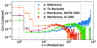
Figure 4 shows the event rate per pixel as a function of multiplicity. It is clear that a large fraction of the events is caused by high multiplicity events in case of chip (blue). In case of chip (orange), (green), and (red), the contribution from high multiplicity events is suppressed and it results in small values of event rate per pixel in Table 1. Note that the probability density of single events () is quite high for all chips, but these events have a negligible contribution to the total dead time per chip. For chip , we have checked that the large value can be explained by statistics: the value is highly changed by changing the threshold of glitch detection. For chip , the large value is the result from scattered events as described in the caption of Fig. 3. For array and , the effect cannot be explained by statistics but may also involve the direct interaction between cosmic rays and the MKID aluminium, without phonon emission and propagation to the next pixel.
We can draw an important conclusion here. If we do not adopt any measure to prevent phonon spread in the chip (as in chip ), the dead time fraction per pixel increases with the array size. On the other hand, a low phonon absorber and/or a membrane structure (chip , , and ) confine the spread of high energy phonons created by cosmic ray events, and the dead time fraction per pixel is independent of the array area: We can make larger-format arrays that do not suffer from significant data loss due to glitches created by cosmic rays. There is another effect of the low layer: When comparing chip (blue, reference) with chip (orange, low layer), we observe a strong reduction in multiplicity. The same effect is observed when comparing the membrane chips: The multiplicity of chip (green, NbTiN ground) is larger than (red, Al ground).
The data and techniques discussed in this letter are important not only for astronomical instruments, but also for quantum computing. The key premises in error-corrected quantum computing are that errors can be sparse enough and therefore minimally correlated, and that logical error rates decrease exponentially with increasing system size Fowler et al. (2012). Cosmic ray events void both. Figure 3 (a) shows how cosmic ray events have generated quasiparticle excitations across the entire chip. For superconducting qubits, the excess quasiparticles can cause deleterious state transitions Wenner et al. (2013); Rainis and Loss (2012), hence cosmic ray events may cause bursts of errors in time across the chip. Moreover, the rate of cosmic ray events goes up with increasing chip size. Completely blocking cosmic rays is impractical. The decrease in event rate displayed in Fig. 3 from using low gap materials and membranes, would carry over to a decrease in transition events associated with excess quasiparticles in superconducting quantum chips. We therefore foresee that mitigating the effects of cosmic rays will become an important part in designing a quantum computer, and hope that the approach taken in this letter can act as guide.
Based on the obtained results, we can estimate the dead time fraction when operating the arrays in an L2 orbit by scaling the event rate on the entire chip (2.5 events/min/cm2) to the event rate of 300 events/min/cm2 that is reported by Planck Planck Collaboration (2014). The calculated values are shown in Table 1. We obtain a dead time fraction of 1.4 % for a monolithic Si (chip ) with size of cm2 and an even smaller value of 0.55 % for chip . These are much smaller than % data loss of Planck that uses Si dies with size of 0.4 to 0.8 cm2 Planck Collaboration (2014); Catalano et al. (2014). We also simulate the energy deposition on a chip by cosmic rays at an L2 orbit assuming the energy spectrum given by Ref. Lotti et al., 2012 (see Fig. 2). Although the primary component of cosmic rays at an L2 orbit is not muons but protons, the peak of the energy deposition from the simulation is almost the same. This indicates that our simple scaling is a reasonable first order approximation. However, the distribution of the deposited energy by protons is much broader with a high energy tail caused by low incident angle protons that travel longer through the Si wafer thereby depositing more energy. In Fig. 2 we also show a simulation of the spectral energy for a vertically placed chip on earth (orange line). This increases the fraction of high deposited energies, at the cost of a much lower interaction rate. For a full understanding of cosmic ray interactions on large MKID arrays, such vertical lab measurements must be combined with dedicated beam line experiments to measure the effect of very high deposited energies which are possible in space.
In conclusion, we demonstrated a method to harden MKID arrays against cosmic ray events by adding a membrane structure and a layer of superconducting material with below or close to the of the Al of the MKIDs. The idea to down-convert energy of phonons fully utilizes the advantage of MKIDs over bolometers: Phonons with energy lower than are invisible to MKIDs. As a result, the dead time fraction per pixel caused by cosmic rays can be reduced up to a factor of 40 with respect to the reference array by a combination of a low layer and a membrane structure. We have shown that these measures reduce the dead time fraction to less than 1 % even at an L2 orbit. The technique described in this paper is important not only for large-format MKID arrays for future astronomical instruments, but also for large qubit arrays for future quantum computers.
Acknowledgements.
We would like to thank E. F. C. Driessen, A. Catalano, M. Calvo for useful discussion, and A. Tokiyasu for advices on GEANT4 simulation. This work was supported by the ERC COG 648135 MOSAIC (J. J. A. B.), NWO Vidi Grant 639.042.423 (A. E.), and NWO Veni Grant 639.041.750 (P. J. de V.).References
- Planck Collaboration (2014) Planck Collaboration, A&A 571, A10 (2014).
- Day et al. (2003) P. K. Day, H. G. LeDuc, B. A. Mazin, A. Vayonakis, and J. Zmuidzinas, Nature 425, 817 (2003).
- Zmuidzinas (2012) J. Zmuidzinas, Annu. Rev. Cond. Mat. Phys. 3, 169 (2012).
- Irwin (1995) K. D. Irwin, Appl. Phys. Lett. 66, 1998 (1995).
- Catalano et al. (2014) A. Catalano, P. Ade, Y. Atik, A. Benoit, E. Bréele, J. J. Bock, P. Camus, M. Chabot, M. Charra, B. P. Crill, N. Coron, A. Coulais, F. X. Désert, L. Fauvet, Y. Giraud-Héraud, O. Guillaudin, W. Holmes, W. C. Jones, J. M. Lamarre, J. Macías-Pérez, M. Martinez, A. Miniussi, A. Monfardini, F. Pajot, G. Patanchon, A. Pelissier, M. Piat, J. L. Puget, C. Renault, C. Rosset, D. Santos, A. Sauvé, L. D. Spencer, and R. Sudiwala, A&A 569, A88 (2014).
- Catalano et al. (2016) A. Catalano, A. Benoit, O. Bourrion, M. Calvo, G. Coiffard, A. D’Addabbo, J. Goupy, H. LeSueur, J. Macías-Pérez, and A. Monfardini, A&A 592 (2016).
- de Visser et al. (2014) P. J. de Visser, J. J. A. Baselmans, J. Bueno, N. Llombart, and T. M. Klapwijk, Nature Communications 5, 3130 (2014).
- Janssen et al. (2013) R. M. J. Janssen, J. J. A. Baselmans, A. Endo, L. Ferrari, S. J. C. Yates, A. M. Baryshev, and T. M. Klapwijk, Appl. Phys. Lett. 103, 203503 (2013).
- Baselmans et al. (2017) J. J. A. Baselmans, J. Bueno, S. J. C. Yates, O. Yurduseven, N. Llombart, K. Karatsu, A. M. Baryshev, L. Ferrari, A. Endo, D. J. Thoen, P. J. de Visser, R. M. J. Janssen, V. Murugesan, E. F. C. Driessen, G. Coiffard, J. Martin-Pintado, P. Hargrave, and M. Griffin, A&A 601 (2017).
- Yates et al. (2017) S. J. C. Yates, A. M. Baryshev, O. Yurduseven, J. Bueno, K. K. Davis, L. Ferrari, W. Jellema, N. Llombart, V. Murugesan, D. J. Thoen, and J. J. A. Baselmans, IEEE Trans. on Terahertz Science and Technology 7, 789 (2017).
- (11) S. Hähnle, O. Yurduseven, S. L. van Berkel, N. Llombart, J. Bueno, S. J. C. Yates, V. Murugesan, D. J. Thoen, A. Neto, and J. J. A. Baselmans, In preparation.
- Bueno et al. (2017) J. Bueno, O. Yurduseven, S. J. C. Yates, N. Llombart, V. Murugesan, D. J. Thoen, A. M. Baryshev, A. Neto, and J. J. A. Baselmans, Appl. Phys. Lett. 110, 233503 (2017).
- Bueno et al. (2018) J. Bueno, V. Murugesan, K. Karatsu, D. J. Thoen, and J. J. A. Baselmans, J. Low Temp. Phys. (2018), 10.1007/s10909-018-1962-8.
- Monfardini et al. (2016) A. Monfardini, J. J. A. Baselmans, A. Benoit, A. Bideaud, O. Bourrion, A. Catalano, M. Calvo, A. D’Addabbo, S. Doyle, J. Goupy, H. L. Sueur, and J. Macias-Perez, Proc. SPIE 9914, 99140 (2016).
- Kozorezov et al. (2000) A. G. Kozorezov, A. F. Volkov, J. K. Wigmore, A. Peacock, A. Poelaert, and R. den Hartog, Phys. Rev. B 61, 11807 (2000).
- Goldie and Withington (2013) D. J. Goldie and S. Withington, Supercond. Sci. Technol. 26, 015004 (2013).
- Holmes et al. (2008) W. A. Holmes, J. J. Bock, B. P. Crill, T. C. Koch, W. C. Jones, A. E. Lange, and C. G. Paine, Appl. Opt. 47, 5996 (2008).
- Baselmans et al. (2012) J. J. A. Baselmans, S. J. C. Yates, P. Diener, and P. J. de Visser, J. Low Temp. Phys. 167, 360 (2012).
- Note (1) Chip and has a gold layer at edges to have a good thermal contact to the gold-plated sample box. The layer is intended to better thermalize the chip under sub-mm illumination Yates et al. (2017).
- van Rantwijk et al. (2016) J. van Rantwijk, M. Grim, D. van Loon, S. J. C. Yates, A. M. Baryshev, and J. J. A. Baselmans, IEEE Trans. on Microwave Theory and Techniques 64, 1876 (2016).
- GEANT4 Collaboration (2003) GEANT4 Collaboration, Nucl. Instrum. Meth. A506, 250 (2003).
- (22) https://nuclear.llnl.gov/simulation/.
- Baselmans et al. (2008) J. J. A. Baselmans, S. J. C. Yates, R. Barends, Y. J. Y. Lankwarden, J. R. Gao, H. Hoevers, and T. M. Klapwijk, J. Low Temp. Phys. 151, 524 (2008).
- (24) https://neutronm.bartol.udel.edu/.
- Fowler et al. (2012) A. G. Fowler, M. Mariantoni, J. M. Martinis, and A. N. Cleland, Phys. Rev. A 86, 032324 (2012).
- Wenner et al. (2013) J. Wenner, Y. Yin, E. Lucero, R. Barends, Y. Chen, B. Chiaro, J. Kelly, M. Lenander, M. Mariantoni, A. Megrant, C. Neill, P. J. J. O’Malley, D. Sank, A. Vainsencher, H. Wang, T. C. White, A. N. Cleland, and J. M. Martinis, Phys. Rev. Lett. 110, 150502 (2013).
- Rainis and Loss (2012) D. Rainis and D. Loss, Phys. Rev. B 85, 174533 (2012).
- Lotti et al. (2012) S. Lotti, E. Perinati, L. Natalucci, L. Piro, T. Mineo, L. Colasanti, and C. Macculi, Nucl. Instrum. Meth. A686, 31 (2012).