Optimized heat transfer at exceptional points in quantum circuits
Abstract
Superconducting quantum circuits are potential candidates to realize a large-scale quantum computer. The envisioned large density of integrated components, however, requires a proper thermal management and control of dissipation. To this end, it is advantageous to utilize tunable dissipation channels and to exploit the optimized heat flow at exceptional points (EPs). Here, we experimentally realize an EP in a superconducting microwave circuit consisting of two resonators. The EP is a singularity point of the Hamiltonian, and corresponds to the most efficient heat transfer between the resonators without oscillation of energy. We observe a crossover from underdamped to overdamped coupling via the EP by utilizing photon-assisted tunneling as an in situ tunable dissipative element in one of the resonators. The methods studied here can be applied to different circuits to obtain fast dissipation, for example, for initializing qubits to their ground states. In addition, these results pave the way towards thorough investigation of parity–time () symmetric systems and the spontaneous symmetry breaking in superconducting microwave circuits operating at the level of single energy quanta.
Systems with effective non-Hermitian Hamiltonians have been actively studied in various setups in recent years Milburn et al. (2015); Xu et al. (2016); Doppler et al. (2016); Mandal and Tewari (2016); Ding et al. (2016, 2018); San-Jose et al. (2016). They show many intriguing properties such as singularities in their energy spectra Kato (1966); Dembowski et al. (2001); Heiss (2004); Berry (2004); Heiss (2012); Cao and Wiersig (2015). A square-root singularity point in the parameter space of a non-Hermitian matrix is called an exceptional point, EP, if the eigenvalues coalesce Heiss (2012); Cao and Wiersig (2015). Previously, EPs have been shown to emerge, for example, in non-superconducting microwave circuits, laser physics, quantum phase transitions, and atomic and molecular physics Heiss (2012); Cao and Wiersig (2015). The fascinating effects of EPs include the disappearance of the beating Rabi oscillations Dietz et al. (2007), chiral states in microwave systems Dembowski et al. (2003), and spontaneous symmetry breaking in systems with parity- and time-reversal () symmetry Bender and Boettcher (1998); Guo et al. (2009); Chtchelkatchev et al. (2012); El-Ganainy et al. (2018). In the quantum regime, -symmetric systems may show features that are different from the semiclassical predictions, such as new phases owing to quantum fluctuations Kepesidis et al. (2016); El-Ganainy et al. (2018). Despite the active research on EPs, they have not been thoroughly investigated in superconducting microwave circuits to date Quijandría et al. (2018).
Superconducting microwave circuits provide an ideal platform to realize various quantum devices, such as ultrasensitive photon detectors and counters Inomata et al. (2016); Govenius et al. (2016); Ding et al. (2017); Opremcak et al. (2018), and potentially even a large-scale quantum computer Ladd et al. (2010); Clarke and Wilhelm (2008), or a quantum simulator Georgescu et al. (2014) in the framework of circuit quantum electrodynamics Blais et al. (2004); Wallraff et al. (2004). Notably, superconducting qubits have been shown to approach the required coherence times Barends et al. (2014); Kelly et al. (2015) for quantum error correction Lidar and Brun (2013); Terhal (2015). However, despite the tremendous interest in superconducting microwave circuits in recent years You and Nori (2011); Devoret and Schoelkopf (2013); Wendin (2017), there are still many issues to be solved before a fully functional quantum computer is possible. For example, the precise engineering of energy flows between different parts of the circuit in scalable architectures is of utmost importance since unwanted heat is a typical source of decoherence in qubits Clerk and Utami (2007); Goetz et al. (2017). In many error correction codes, qubits are repeatedly initialized, which requires fast and efficient cooling schemes Geerlings et al. (2013); Bultink et al. (2016); Wong et al. (2018). One promising method for absorbing energy and initializing qubits to their ground state is based on resonators with tunable dissipation Tuorila et al. (2017).
The recently developed quantum-circuit refrigerator (QCR) Tan et al. (2017); Masuda et al. (2018) provides great potential for both qubit initialization and thermal management since it enables tunability of energy dissipation rates over several orders of magnitude in a superconducting microwave resonator Silveri et al. (2018). Operation of the QCR relies on inelastic tunneling of electrons through a normal-metal–insulator–superconductor (NIS) junction Silveri et al. (2017). The tunneling electrons can absorb or emit photons to a resonator which allows to control the coupling strength to a low-temperature bath in situ. This tunable coupling strength has also been shown to induce a broadband Lamb shift Silveri et al. (2018). Furthermore, elastic tunneling can be utilized for temperature control of the normal-metal electrons Nahum et al. (1994); Leivo et al. (1996); Giazotto et al. (2006), and for precise thermometry down to millikelvin temperatures Feshchenko et al. (2015); Giazotto et al. (2006). Recently, NIS junctions have also been utilized in a realization of a quantum heat valve Ronzani et al. (2018), and phase-coherent caloritronics Fornieri and Giazotto (2017).
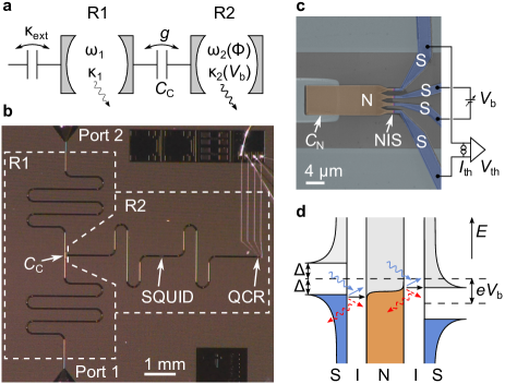
In this work, we combine the advantages of tunable dissipation and EPs to optimize the heat flow in a superconducting microwave circuit. To this end, we investigate a circuit consisting of two coupled resonators, one of which is equipped with NIS junctions and a flux-tunable resonance frequency (Fig. 1). We denote the NIS junctions and the normal-metal island that is capacitively coupled to the resonator as a QCR. Thanks to the voltage-tunable dissipation within the QCR and the flux-tunable resonance frequency, an EP arises in the Hamiltonian that describes the modes of the coupled resonator system. We investigate the emergence of the EP using frequency and dissipation as control parameters (Fig. 2) and verify its properties experimentally by measuring the microwave transmission coefficient (Fig. 3). The optimal heat flow given by the coupling strength can be reached at the EP (Fig. 4). Different types of tunable resonators have been studied in recent years Wang et al. (2013); Pierre et al. (2014); Baust et al. (2015); Vissers et al. (2015); Wulschner et al. (2016); Adamyan et al. (2016); Pierre et al. (2018); Wong et al. (2018); Partanen et al. (2018) but not with voltage-tunable dissipation. Our work demonstrates a platform to control the local heat transport between neighboring nodes in a quantum electrical circuit. In addition to thermal management within superconducting multi-qubit systems, these methods may be applicable to thermally assisted quantum annealing Dickson et al. (2013) and to studies of the eigenstate thermalization hypothesis in many-body quantum problems Nandkishore and Huse (2015). Furthermore, our work is an important step towards the investigation of -symmetric systems at the quantum level that can be realized with circuit quantum electrodynamics architectures Metelmann and Türeci (2018); Quijandría et al. (2018).
Results
Experimental samples
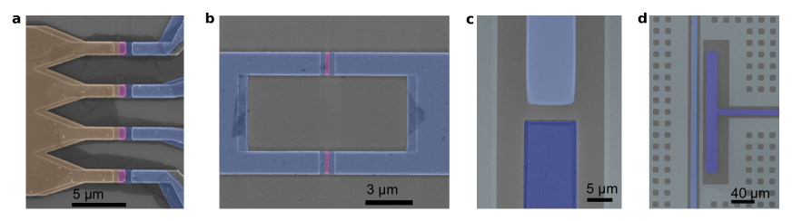
Our samples consist of two coplanar waveguide resonators, R1 and R2, which are capacitively coupled to each other, as depicted in Fig. 1(a), (b) (see also Supplementary Fig. S1). The resonator R1 has a fixed fundamental frequency at . This mode does not couple strongly to the resonator R2 owing to the voltage node in the middle of the resonator R1 where the coupling capacitor is located. Therefore, we focus on the first excited mode of R1, with frequency , which has a voltage antinode at the coupling point of the resonators. The resulting capacitive coupling between the resonators has a strength . In contrast to R1, the resonator R2 has a flux-tunable resonance frequency owing to a superconducting quantum interference device (SQUID), and a voltage tunable loss rate owing to the QCR. Here, and are the magnetic flux applied to the SQUID loop and the voltage bias of the QCR, respectively. The inductance of the SQUID and, hence, also the resonance frequency of R2 are periodic in flux with a period of the flux quantum . Consequently, due to the coupling of the resonators, R1 also shows flux-dependent features. We show the QCR in Fig. 1(c) and schematically present its operation principle in Fig. 1(d). The difference in photon absorption and emission rates originates from the gap of in the density of states of the superconductor, and the difference can be utilized to cool down quantum circuits Tan et al. (2017); Silveri et al. (2017). The sample fabrication is described in Methods. We study two samples with different R2 resonator lengths, Sample A () and Sample B (). The R1 resonator has a length of in both samples. Sample parameters are summarized in Supplementary Table S1.
Exceptional points
To study exceptional points, we utilize two control parameters in the effective Hamiltonian of the system: we use the voltage-tunable dissipation rate and the flux-tunable detuning between the resonators . We study the system consisting of the two resonators in a rotating frame with a frequency corresponding to the uncoupled mode frequency of R1, similarly as in Ref. Doppler et al. (2016). Thus, the excitations of the system can be described with the effective non-Hermitian Hamiltonian in matrix form in the basis where and are field amplitudes in R1 and R2, respectively, (see Methods and Ref. Pierre et al. (2018))
| (1) |
where is the decay rate of the resonator R1. The eigenvalues of can be written as
| (2) |
and the corresponding eigenvectors are
| (3) |
where
| (4) |
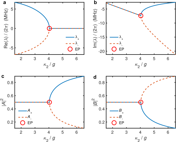
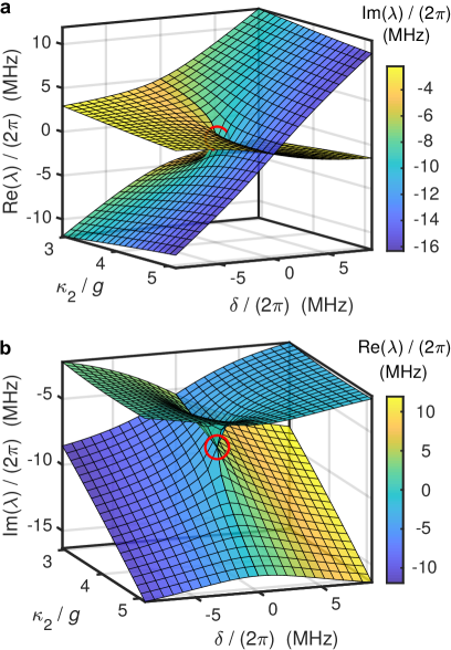
Thus, the eigenvalues and eigenvectors coalesce when the square-root term vanishes resulting in an EP. Consequently, there is only a single eigenvalue and, importantly, there is also only a single eigenvector. The EP occurs at , and . In the following, we assume that , which is valid for our samples, as discussed below. Consequently, the condition for the EP simplifies to .
To visualize the system singularity, i.e., the EP, we show the real and imaginary parts of in Fig. 2. The eigenvalues form a self-intersecting Riemann surface in the parameter space of and . The imaginary part corresponds to mode decay, and real part to mode frequency deviation from the uncoupled mode frequency of R1. Our system consisting of the resonators R1 and R2 can be considered as a single damped harmonic oscillator, where the energy oscillates between the two resonators. In the underdamped case, , the modes have an equal decay rate at zero detuning, and there is an anti-crossing of the mode frequencies. In contrast, in the overdamped case, , there is an anticrossing in the mode decay rates as a function of the detuning, and the mode frequencies are equal at zero detuning. Consequently, one of the modes remains lossy whereas the other one has a low decay rate at different detunings.
Let us connect the meaning of this critical point to the efficiency of energy transfer between the two resonators. In terms of coupled dissipative systems, the EP separates the system between the overdamped and underdamped regime being the point of critical coupling. It follows from the dynamics of the coupled system that at this point the energy is transfered between the two resonators optimally fast without back and forth oscillation Pierre et al. (2018); Wong et al. (2018). In particular, the rate of heat transfer at zero detuning is given by . Here, the branch with the upper signs corresponds to a mode located predominantly in the primary resonator R1, and the branch with the lower ones in the dissipative resonator R2 (Supplementary Fig. S2). Consequently, by reaching the EP at , we operate our sample at a point of optimally efficient and nonreciprocal heat transfer out of R1.
Experimental observations
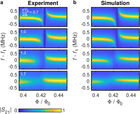
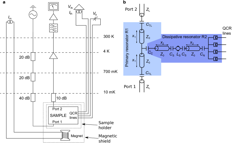
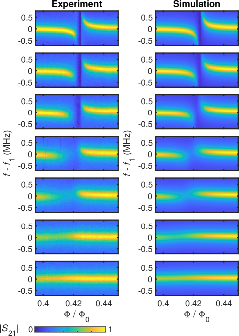
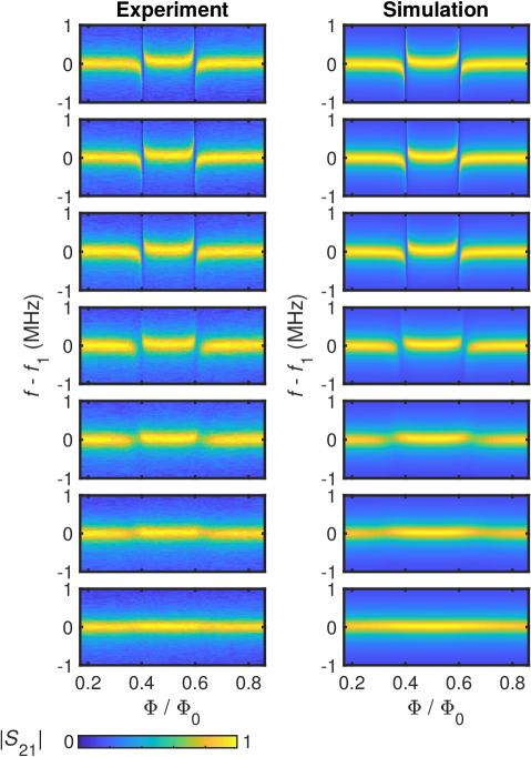
To explore the dissipative dynamics of the two coupled resonators, we measure the flux- and frequency-dependent scattering parameter describing the transmission from Port 1 to Port 2 for different bias voltages using a vector network analyzer. We tune the magnetic flux in a range where the frequency of R2 crosses that of R1. As shown in Fig. 3(a), we observe a transition from anticrossing to a single mode already indicating the presence of an EP in-between. A broader range of bias voltages is shown in Supplementary Figs. S4 and S5. To generate a quantitative description of our system, which is required for the investigation of EPs, we numerically simulate the scattering coefficient as shown in Fig. 3(b). Here, we model the SQUID as a flux-tunable inductor, and the QCR as an effective resistance (see Methods and Supplementary Fig. S3). We extract by fitting the circuit model to the experimental results, and use to obtain the damping rates of the dissipative resonator R2 as a function of the bias voltage (Methods). The extracted resistances are given in Supplementary Fig. S6. The model in Fig. 3 is in very good agreement with the experimental results. In addition to , we also extract the coupling capacitance and the critical current of the SQUID from the simulation. The coupling capacitance is found to be which agrees well with the finite-element-method simulation that yields approximately .
In Fig. 3(a) the crossing of the modes as a function of the flux shifts slightly towards lower flux values. We attribute this shift to heating of the SQUID, which results in a reduced critical current of the SQUID, and hence a larger inductance and lower resonance frequency of R2. In principle, we vary also the Lamb shift Silveri et al. (2018), which, however, causes only a minor effect since the resonance of R2 is very broad, and therefore, we neglect it in our model. To verify our above assumption , we measure the internal quality factor of the primary resonator R1 with R2 far detuned at . From the quality factor, we extract a loss rate for both samples which is substantially lower than the extracted value of . We measure a slight temperature and power dependence of the quality factor of R1 as expected in the case of two-level fluctuators dominating the losses Zmuidzinas (2012) (Supplementary Fig. S8).
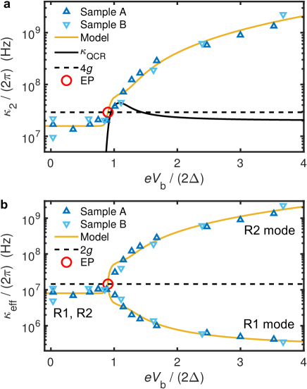
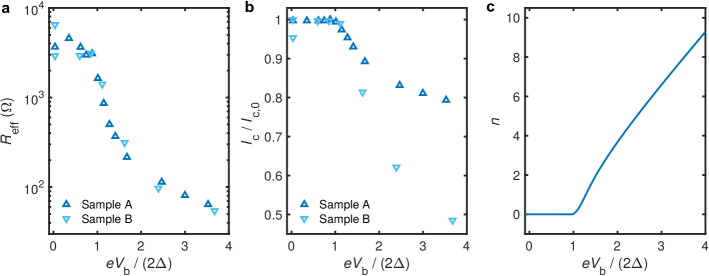
To demonstrate the presence of an EP, we show the extracted damping rates (Methods) of the bare resonator R2 in the absence of R1 in Fig. 4(a) as functions of the bias voltage for Samples A and B. Both samples have similar damping rates and . The value of can be tuned by approximately two orders of magnitude. At low bias voltages , the rate is below , and at the damping rate exceeds . We describe the origin of the tunable damping rates using a model that contains the photon absorption and emission at the QCR given by the rate , as well as constant internal losses , and voltage-dependent residual losses . We have designed our sample in such a way that covers the critical damping rate, and thus the losses originating from the QCR are sufficient to realize the EP. The damping rate shown in Fig. 4 is calculated using the measured electron temperatures of the normal-metal island (see Methods and Supplementary Fig. S7). At higher voltages, the major contribution in is given by the residual damping coefficient, as discussed in Methods. This damping coefficient includes dephasing, quasiparticle losses, and resistive losses, and we extract its value based on the experimental rates. The dephasing has a similar effect on the measured coherent photon population as photon absorption due to other loss mechanisms although pure dephasing does not reduce the total photon number in the resonators.
In Fig. 4(b) we show the damping rates of the coupled circuit calculated from using Eq. (2) as . The maximum energy decay rate for the mode in R1 is obtained at the EP as discussed above, and it is given by . Thus, in the optimal case, the decay rate is limited by the coupling strength between the resonators.
Discussion
We have experimentally realized an exceptional point, EP, in a superconducting microwave circuit. We study the presence of the EP by observing a transition from an avoided crossing to single modulating resonance frequency. At this point, we achieve a maximum heat transfer between the two resonators without back and forth oscillation of the energy. The effective dissipation rate of the resonator R1 is bounded from above by the coupling strength in the optimal case, . In the far detuned case with zero bias voltage, the effective rate of R1 is reduced down to . Thus, the effective damping rate can be tuned by a factor of approximately 50 in our samples. Larger tuning can be obtained by minimizing the internal losses Megrant et al. (2012). The measurement results are in very good agreement with our model. The circuit is based on a QCR, which enables the investigation of the crossover from an underdamped to critically damped and further to overdamped circuit. In addition to the realization of an EP, the circuit also behaves as a frequency- and voltage-tunable heat sink for quantum electric circuits that can be applied, for example, in quantum information processing for initializing qubits to their ground state by absorbing energy Tuorila et al. (2017). The tunability of the damping rate enables one to obtain the fastest possible photon absorption allowed by a given coupling coefficient.
In the future, it is interesting to further investigate the EP by modifying the circuit design. By introducing tunnel junctions to both resonators, one obtains a continuous line of EPs instead of an isolated singularity point. Incorporating qubits also enables the investigation and utilization of the EP with single energy quanta. Furthermore, one can investigate a circuit consisting of resonators with tunable damping realized with a QCR and a tunable coupling realized with a SQUID or a qubit Baust et al. (2015); Wulschner et al. (2016). The use of several microwave resonators will result in a more versatile parameter space Demange and Graefe (2012), and hence yields an interesting platform for studying fundamental physics. Dynamic encircling of the EP with topological energy transfer Dembowski et al. (2001); Doppler et al. (2016) can be realized with superconducting resonators in a straightforward manner using standard microwave techniques. It requires fast tuning of the magnetic field, which can be realized by fabricating a flux bias line on the chip. Topological energy transfer with microwave pulses may provide an asset for applications in quantum information processing and other quantum technological devices. In addition, EPs are suitable for investigating symmetry on the level of single microwave photons. Here, superconducting circuits provide an attractive architecture owing to the ability to design system parameters yielding, for example, ultra-strong- and deep-strong-coupling regimes Quijandría et al. (2018). Furthermore, we see EPs as candidates to realize nonreciprocal signal routing beneficial for active quantum circuits Metelmann and Türeci (2018).
References
- Milburn et al. (2015) T. J. Milburn, J. Doppler, C. A. Holmes, S. Portolan, S. Rotter, and P. Rabl, Phys. Rev. A 92, 052124 (2015).
- Xu et al. (2016) H. Xu, D. Mason, L. Jiang, and J. G. E. Harris, Nature 537, 80 (2016).
- Doppler et al. (2016) J. Doppler et al., Nature 537, 76 (2016).
- Mandal and Tewari (2016) I. Mandal and S. Tewari, Physica E: Low Dimens. Syst. Nanostruct. 79, 180 (2016).
- Ding et al. (2016) K. Ding, G. Ma, M. Xiao, Z. Q. Zhang, and C. T. Chan, Phys. Rev. X 6, 021007 (2016).
- Ding et al. (2018) K. Ding, G. Ma, Z. Q. Zhang, and C. T. Chan, Phys. Rev. Lett. 121, 085702 (2018).
- San-Jose et al. (2016) P. San-Jose, J. Cayao, E. Prada, and R. Aguado, Sci. Rep. 6, 21427 (2016).
- Kato (1966) T. Kato, Perturbation theory for linear operators, Grundlehren der mathematischen Wissenschaften, Vol. 132 (Springer-Verlag Berlin Heidelberg, Gießen, 1966).
- Dembowski et al. (2001) C. Dembowski, H.-D. Gräf, H. L. Harney, A. Heine, W. D. Heiss, H. Rehfeld, and A. Richter, Phys. Rev. Lett. 86, 787 (2001).
- Heiss (2004) W. Heiss, Czech. J. Phys. 54, 1091 (2004).
- Berry (2004) M. Berry, Czech. J. Phys. 54, 1039 (2004).
- Heiss (2012) W. D. Heiss, J. Phys. A: Math. Theor. 45, 444016 (2012).
- Cao and Wiersig (2015) H. Cao and J. Wiersig, Rev. Mod. Phys. 87, 61 (2015).
- Dietz et al. (2007) B. Dietz, T. Friedrich, J. Metz, M. Miski-Oglu, A. Richter, F. Schäfer, and C. A. Stafford, Phys. Rev. E 75, 027201 (2007).
- Dembowski et al. (2003) C. Dembowski, B. Dietz, H.-D. Gräf, H. L. Harney, A. Heine, W. D. Heiss, and A. Richter, Phys. Rev. Lett. 90, 034101 (2003).
- Bender and Boettcher (1998) C. M. Bender and S. Boettcher, Phys. Rev. Lett. 80, 5243 (1998).
- Guo et al. (2009) A. Guo et al., Phys. Rev. Lett. 103, 093902 (2009).
- Chtchelkatchev et al. (2012) N. M. Chtchelkatchev, A. A. Golubov, T. I. Baturina, and V. M. Vinokur, Phys. Rev. Lett. 109, 150405 (2012).
- El-Ganainy et al. (2018) R. El-Ganainy, K. G. Makris, M. Khajavikhan, Z. H. Musslimani, S. Rotter, and D. N. Christodoulides, Nat. Phys. 14, 11 (2018).
- Kepesidis et al. (2016) K. V. Kepesidis, T. J. Milburn, J. Huber, K. G. Makris, S. Rotter, and P. Rabl, New J. Phys. 18, 095003 (2016).
- Quijandría et al. (2018) F. Quijandría, U. Naether, S. K. Özdemir, F. Nori, and D. Zueco, Phys. Rev. A 97, 053846 (2018).
- Inomata et al. (2016) K. Inomata, Z. Lin, K. Koshino, W. D. Oliver, J.-S. Tsai, T. Yamamoto, and Y. Nakamura, Nat. Commun. 7, 12303 (2016).
- Govenius et al. (2016) J. Govenius, R. E. Lake, K. Y. Tan, and M. Möttönen, Phys. Rev. Lett. 117, 030802 (2016).
- Ding et al. (2017) J. Ding et al., IEEE T. Appl. Supercon. 27, 1 (2017).
- Opremcak et al. (2018) A. Opremcak et al., Science 361, 1239 (2018).
- Ladd et al. (2010) T. D. Ladd, F. Jelezko, R. Laflamme, Y. Nakamura, C. Monroe, and J. L. O’Brien, Nature 464, 45 (2010).
- Clarke and Wilhelm (2008) J. Clarke and F. K. Wilhelm, Nature 453, 1031 (2008).
- Georgescu et al. (2014) I. M. Georgescu, S. Ashhab, and F. Nori, Rev. Mod. Phys. 86, 153 (2014).
- Blais et al. (2004) A. Blais, R.-S. Huang, A. Wallraff, S. M. Girvin, and R. J. Schoelkopf, Phys. Rev. A 69, 062320 (2004).
- Wallraff et al. (2004) A. Wallraff et al., Nature 431, 162 (2004).
- Barends et al. (2014) R. Barends et al., Nature 508, 500 (2014).
- Kelly et al. (2015) J. Kelly et al., Nature 519, 66 (2015).
- Lidar and Brun (2013) D. Lidar and T. Brun, eds., Quantum Error Correction (Cambridge University Press, 2013).
- Terhal (2015) B. M. Terhal, Rev. Mod. Phys. 87, 307 (2015).
- You and Nori (2011) J. Q. You and F. Nori, Nature 474, 589 (2011).
- Devoret and Schoelkopf (2013) M. H. Devoret and R. J. Schoelkopf, Science 339, 1169 (2013).
- Wendin (2017) G. Wendin, Rep. Prog. Phys. 80, 106001 (2017).
- Clerk and Utami (2007) A. A. Clerk and D. W. Utami, Phys. Rev. A 75, 042302 (2007).
- Goetz et al. (2017) J. Goetz et al., Phys. Rev. Lett. 118, 103602 (2017).
- Geerlings et al. (2013) K. Geerlings et al., Phys. Rev. Lett. 110, 120501 (2013).
- Bultink et al. (2016) C. C. Bultink et al., Phys. Rev. Appl. 6, 034008 (2016).
- Wong et al. (2018) C. H. Wong, C. Wilen, R. McDermott, and M. G. Vavilov, Preprint, arXiv:1806.01880 (2018).
- Tuorila et al. (2017) J. Tuorila, M. Partanen, T. Ala-Nissila, and M. Möttönen, npj Quantum Inf. 3, 27 (2017).
- Tan et al. (2017) K. Y. Tan, M. Partanen, R. E. Lake, J. Govenius, S. Masuda, and M. Möttönen, Nat. Commun. 8, 15189 (2017).
- Masuda et al. (2018) S. Masuda et al., Sci. Rep. 8, 3966 (2018).
- Silveri et al. (2018) M. Silveri et al., Preprint, arXiv:1809.00822 (2018).
- Silveri et al. (2017) M. Silveri, H. Grabert, S. Masuda, K. Y. Tan, and M. Möttönen, Phys. Rev. B 96, 094524 (2017).
- Nahum et al. (1994) M. Nahum, T. M. Eiles, and J. M. Martinis, Appl. Phys. Lett. 65, 3123 (1994).
- Leivo et al. (1996) M. M. Leivo, J. P. Pekola, and D. V. Averin, Appl. Phys. Lett. 68, 1996 (1996).
- Giazotto et al. (2006) F. Giazotto, T. T. Heikkilä, A. Luukanen, A. M. Savin, and J. P. Pekola, Rev. Mod. Phys. 78, 217 (2006).
- Feshchenko et al. (2015) A. V. Feshchenko et al., Phys. Rev. Applied 4, 034001 (2015).
- Ronzani et al. (2018) A. Ronzani, B. Karimi, J. Senior, Y.-C. Chang, J. T. Peltonen, C. Chen, and J. P. Pekola, Nat. Phys. 14, 991 (2018).
- Fornieri and Giazotto (2017) A. Fornieri and F. Giazotto, Nat. Nanotechnol. 12, 944 (2017).
- Wang et al. (2013) Z. L. Wang, Y. P. Zhong, L. J. He, H. Wang, J. M. Martinis, A. N. Cleland, and Q. W. Xie, Appl. Phys. Lett. 102, 163503 (2013).
- Pierre et al. (2014) M. Pierre, I.-M. Svensson, S. R. Sathyamoorthy, G. Johansson, and P. Delsing, Appl. Phys. Lett. 104, 232604 (2014).
- Baust et al. (2015) A. Baust et al., Phys. Rev. B 91, 014515 (2015).
- Vissers et al. (2015) M. R. Vissers, J. Hubmayr, M. Sandberg, S. Chaudhuri, C. Bockstiegel, and J. Gao, Appl. Phys. Lett. 107, 062601 (2015).
- Wulschner et al. (2016) F. Wulschner et al., EPJ Quantum Technol 3, 10 (2016).
- Adamyan et al. (2016) A. A. Adamyan, S. E. Kubatkin, and A. V. Danilov, Appl. Phys. Lett. 108, 172601 (2016).
- Pierre et al. (2018) M. Pierre, S. R. Sathyamoorthy, I.-M. Svensson, G. Johansson, and P. Delsing, Preprint, arXiv:1802.09034 (2018).
- Partanen et al. (2018) M. Partanen et al., Sci. Rep. 8, 6325 (2018).
- Dickson et al. (2013) N. G. Dickson et al., Nat. Commun. 4, 1903 (2013).
- Nandkishore and Huse (2015) R. Nandkishore and D. A. Huse, Annu. Rev. Condens. Matter Phys. 6, 15 (2015).
- Metelmann and Türeci (2018) A. Metelmann and H. E. Türeci, Phys. Rev. A 97, 043833 (2018).
- Zmuidzinas (2012) J. Zmuidzinas, Annu. Rev. Condens. Matter Phys. 3, 169 (2012).
- Megrant et al. (2012) A. Megrant et al., Appl. Phys. Lett. 100, 113510 (2012).
- Demange and Graefe (2012) G. Demange and E.-M. Graefe, J. Phys. A: Math. Theor. 45, 025303 (2012).
- Pekola et al. (2010) J. P. Pekola et al., Phys. Rev. Lett. 105, 026803 (2010).
- Jones et al. (2013) P. J. Jones, J. Salmilehto, and M. Möttönen, J. Low Temp. Phys. 173, 152 (2013).
- Göppl et al. (2008) M. Göppl et al., J. Appl. Phys. 104, 113904 (2008).
- Oelsner et al. (2017) G. Oelsner et al., Phys. Rev. Appl. 7, 014012 (2017).
- Barends et al. (2011) R. Barends et al., Appl. Phys. Lett. 99, 113507 (2011).
- O’Neil et al. (2012) G. C. O’Neil, P. J. Lowell, J. M. Underwood, and J. N. Ullom, Phys. Rev. B 85, 134504 (2012).
- Pozar (2011) D. Pozar, Microwave Engineering, 4th ed. (John Wiley & Sons, Hoboken, 2011).
- Petersan and Anlage (1998) P. J. Petersan and S. M. Anlage, J. Appl. Phys. 84, 3392 (1998).
Acknowledgements
We thank A. A. Clerk for discussions, and J. Govenius and M. Jenei for assistance. We acknowledge the provision of facilities and technical support by Aalto University at OtaNano - Micronova Nanofabrication Centre. We acknowledge the funding from the European Research Council under Consolidator Grant No. 681311 (QUESS), and Marie Skłodowska-Curie Grant No. 795159, the Academy of Finland through its Centres of Excellence Program (project Nos. 312300, 312059) and grants (Nos. 265675, 305237, 305306, 308161, 312300, 314302, 316551), the Vilho, Yrjö and Kalle Väisälä Foundation, the Technology Industries of Finland Centennial Foundation, the Jane and Aatos Erkko Foundation the Alfred Kordelin Foundation, and the Emil Aaltonen Foundation.
Author contributions
M.P. was responsible for sample design, fabrication, measurements, data analysis, and writing the manuscript. K.Y.T, and J.G. contributed to the sample design. L.G. deposited the Nb layer. J.G., V.S., K.K., and K.Y.T. contributed to measurements and data analysis. M.P., K.Y.T, and R.E.L. developed the fabrication process. V.V., R.K., J.I., and D.H. contributed to the measurements. M.P.S., A.M., and E.H. contributed to the theory. M.M. supervised the project. All authors commented on the manuscript.
Methods
Quantum-circuit refrigerator
We use a QCR to absorb and emit photons in the resonator R2. The resonator transition rate from the occupation number to can be written as Silveri et al. (2017)
| (5) |
where , is the tunneling resistance, is the corresponding matrix element, k is the von Klitzing constant, and the normalized rate for forward tunneling is given by
| (6) |
where is the Fermi–Dirac distribution, is the Boltzmann constant, and the density of states in a superconductor can be expressed with the help of the Dynes parameter as
| (7) |
The matrix element describing the transition can be written in terms of the generalized Laguerre polynomials as Silveri et al. (2017)
| (8) |
where is a environmental parameter, where is the capacitance per unit length of the coplanar waveguide, is the length of the resonator R2, and the capacitance fraction is given in terms of the capacitance between the normal-metal island and the center conductor , and junction capacitance as . In the equations above, we have neglected the effects owing to the charging of the normal-metal island since the capacitance of the island is relatively large. Furthermore, the rates for single-photon transitions can be expressed as Silveri et al. (2017)
| (9) | |||||
where denotes the coupling strength of the QCR, and the Bose–Einstein distribution at the effective temperature of the electron tunneling, , is given by
| (10) |
where
| (11) |
These equations are derived by defining
| (12) |
Elastic tunneling in normal-metal–insulator–superconductor junctions
Typically, the elastic tunneling is the dominating tunneling process. The electric current through a single NIS junction can be written as Giazotto et al. (2006); Pekola et al. (2010)
| (13) |
where denotes the normal-metal temperature, and is the voltage across the junction. For a symmetric SINIS structure, we apply a voltage . Importantly, this equation has a monotonic dependence on the temperature of the normal metal but only a very weak dependence on the temperature of the superconductor. Thus, we may use NIS junctions as thermometers measuring the electron temperature of the normal metal.
The tunneling electrons transfer heat through the insulating barrier. The average power is given by Giazotto et al. (2006)
| (14) |
Based on this equation, we can reduce and increase the temperature of the normal metal. The applied voltage at the SINIS junction produces a total Joule heating power , which is unequally divided between the N and S electrodes.
Quantum mechanical model
We analyze the temporal evolution of the coupled resonators following Ref. Pierre et al. (2018). The Hamiltonian can be written in the rotating wave approximation as
| (15) |
The first term describes the energy of the primary resonator R1 with annihilation operator , the second term the energy of R2 with annihilation operator , and the third term describes the coupling between the resonators. Here, we have neglected driving. Furthermore, this equation is valid only for a linear resonator. The effects owing to nonlinearity are discussed below. The dynamics of the system can be obtained from the Lindblad master equation for the density matrix of the coupled system, , as
| (16) |
where the Lindblad superoperator is given by . We can write the resulting equations of motion as Pierre et al. (2018)
| (17) | |||||
| (18) |
We define the resonator fields as , . Consequently, the equations assume the form
| (19) | |||||
| (20) |
where . These equations can be written in a matrix form as a time-dependent Schrödinger equation
| (21) |
where , and
| (22) |
as given in Eq. (1). Here, is a non-Hermitian Hamiltonian scaled with . Equations (19) and (20) can also be written as a second-order differential equation,
| (23) |
When the resonators are tuned into resonance, , we can express Eq. (23) as
| (24) |
This equation describes a damped harmonic oscillator, where the energy is transferred between the resonators R1 and R2 at an angular frequency . Due to the asymmetric damping rates in the two resonators, the total dissipation rate of the system is time-dependent and reaches its maximum value when the excitations are in R2. The damping ratio is given by
| (25) |
Here, is a function of voltage , which allows us to examine the transition from an underdamped system, , through critical damping, , to an overdamped system, . Critical damping is obtained when . The total damping rate of R1 is given by , and of R2 by , where denote the internal losses, the losses to the external measurement circuit, the photon-assisted tunneling in Eq. (12), and the residual voltage-dependent losses in R2. In our samples , and , as discussed below. Therefore, we obtain an approximate condition for the critical damping as
| (26) |
The critical damping, which corresponds to the EP, is obtained at where the photon number remains low, and therefore, the slight nonlinearity caused by the SQUID is of negligible importance. However, at , the QCR generates thermal photons that result in photon-number-dependent losses, as discussed below.
Sample parameters
The main parameters for the samples are summarized in Supplementary Table S1. The coupling strength between the resonators can be estimated as Jones et al. (2013) , where the voltages are given by , , the angular frequency of the second mode of the resonator R1 is for Samples A and B, and is the capacitance per unit length. Consequently, the critical damping is obtained with . The external quality factor corresponding to the leakage from the resonator R1 to the transmission line through the capacitances is given by Göppl et al. (2008) . Consequently, the corresponding damping rate is . The loaded quality factor of the second mode of R1 is approximately , when the resonators are far detuned. Thus, the internal losses in R1 dominate over the losses to the transmission line, . Furthermore, we obtain the damping rate . The real part of the complex wave propagation coefficient, , describes the damping in the waveguide, and it can be calculated as Göppl et al. (2008) , where is the mode number with denoting the first excited mode. The internal losses without the photon-assisted tunneling in the QCR are somewhat higher in the resonator R2 than in R1 since the design and fabrication of the QCR and the SQUID have not been optimized for low loss rates. The internal loss rate for R2 can be extracted at zero detuning and zero bias voltage from the saturation level of extracted values since , and hence the losses in R2 dominate over those in R1. We obtain from the circuit model the internal loss rate for R2 as .
The photon number inside R1 when R2 is far detuned can be estimated as Oelsner et al. (2017) , where the driving strength is given by , the input voltage is obtained from the input power as , and the input power is dBm. The input power is dBm for Sample A in Fig. 3 and Supplementary Fig. S4, and dBm for Sample B in Supplementary Fig. S5. We also measure the resonators at different power levels. When R1 and R2 are in resonance at , the total photon number is approximately equally divided between the resonators if . However, in our samples , especially at , and therefore the number of coherent photons is lower in R2 than in R1. When the factor of the resonator is reduced to 200, which is of the order of the critical damping, photon numbers close to unity are obtained with an input power dBm.
Residual losses in the resonator R2
We attribute the residual voltage-dependent losses to dephasing, and to dissipation sources such as quasiparticle generation in the superconductors and resistive losses in the normal metal. Firstly, the resonator R2 is slightly nonlinear owing to the SQUID, and hence, an increasing incoherent photon number results in dephasing. Dephasing can be added in Eq. (16) with a term , where the dephasing rate depends on the number of thermal photons in the resonator. Similarly, in the case of superconducting qubits, the dephasing can be written as , where is a Pauli operator. The factor causes a similar effect as in Eqs. (16)–(26) although it does not decrease the total photon number in the resonators. The photon number variance for a thermal state is of the form Clerk and Utami (2007); Goetz et al. (2017) , and therefore, thermal photons cause more dephasing than the coherent photons with a variance of , where is the average photon number. Consequently, we assume that , where is a proportionality coefficient. Furthermore, as discussed above, the number of the coherent photons is low in R2 due to the relatively high loss rate. The steady-state photon number in the resonator can be estimated as Silveri et al. (2017)
| (27) |
where we assume that the photon number of the effective bath, to which R2 is coupled through , vanishes owing to the very low cryostat temperatures of approximately . The photon number depends linearly on the bias voltage at voltages above the superconductor energy gap, as shown in Supplementary Fig. S6.
Secondly, we take the quasiparticle losses into account. The critical temperature of Nb is approximately , and therefore, the quasiparticle density remains low in it. However, the critical temperature of Al approximately , which enables higher quasiparticle density than in Nb. We observe a decrease in the critical current of the SQUID, which indicates increased temperature in the Al leads of the SQUID, and hence heat dissipation. The quasiparticle loss rate Barends et al. (2011); O’Neil et al. (2012) , where is the absorbed power. The Al leads at the NIS junctions receive half of the Joule power at high voltages, whereas the other half is absorbed to the normal metal. Thus, the power is quadratic in voltage, which is linear in the estimated photon number. Therefore, the expected quasiparticle losses are linear in photon number, , where is a proportionality coefficient. The dc power dissipated in the junctions is substantially higher than the microwave input power. At , the dc power is approximately compared to a microwave power of . The normal metal in the QCR acts as an effective quasiparticle trap O’Neil et al. (2012) minimizing the quasiparticle losses. Some fraction of the power dissipated at the QCR leaks to the SQUID.
There is an approximately 10-m-long section of normal metal between the actual Nb resonator and the NIS junctions, which may cause some losses. The loss rate at the resistor depends on the current profile of the microwave mode, which can depend on the voltage . Nevertheless, we assume these losses to be small due to the QCR being at the end of the resonator. Furthermore, there is a layer of superconducting Al below the normal metal due to the shadow evaporation technique, which decreases the current in the resistor, and hence also the resistive losses. The very weak resistive losses are quadratic in the voltage amplitude of the microwave resonator which is linear in photon number. Thus, it can be approximated as with a proportionality coefficient .
Consequently, the total voltage-dependent losses in R2 including the dephasing, quasiparticle losses in the superconductors and the resistive losses are given by
| (28) |
The quasiparticle and resistive losses are expected to be very weak, as described above, but a small contribution cannot be excluded. Nevertheless, we expect the dephasing to dominate over the quasiparticle and resistive losses. Therefore, in the numerical analysis, we take the photon-number-dependent losses into account as
| (29) |
with only one fitting parameter effectively describing the different loss methods discussed above. From the experimental damping rates of the dissipative resonator R2, we extract the the coefficient . The good agreement with the experimental damping rate and the model with the quadratic residual losses in Fig. 4(a) gives further support for the approximation in Eq. (29). We do not take this loss rate into account in Eq. (27) for simplicity, and also due to the fact that pure dephasing does not decrease the photon number.
The odd modes of R1 do not show flux dependence as expected due to the voltage node at the coupling capacitor. However, they do show some dependence on the voltage . Similar dependence can be observed also for the even modes at where the inductance of the SQUID ideally vanishes and thus decouples the QCR from the resonator R1. We attribute this observation to unintentional asymmetry of the sample. Furthermore, the QCR may be weakly coupled to the input and output microwave fields through some spurious mode of the sample holder. The very broad resonance at high bias voltages enables the coupling to the spurious modes. We note that the spurious modes may be partially responsible for the . However, we do not quantitatively model these losses. Instead, they are effectively included in the parameter in Eq. (29).
Full model for and
The parameters and are obtained as follows. First, we extract the effective resistance corresponding to the QCR by fitting the classical circuit model to the experimentally obtained scattering parameter using a least-squares algorithm. Second, we calculate the quality factor of the resonator R2, , for the obtained effective resistance, as discussed below. The coupling rate is related to the quality factor as . The full model denoted by the line in Fig. 4(a) is obtained by fitting
| (30) |
to the experimental transition rates according to Eqs. (12), (27), and (29). Here, we use as the only fitting parameter since we fix to the saturation value at zero bias, as discussed above.
Classical circuit model
To simulate the scattering parameter , we use a classical circuit model similar to the one presented in Ref. Partanen et al. (2018). We analyze the samples using standard microwave circuit analysis Pozar (2011). The input impedance of the resonator R2 is
| (31) |
where the impedance of the SQUID and the capacitors between the SQUID and the center conductor is given by , the impedance of the coupling capacitor between the resonators by , is the complex propagation coefficient discussed above, and the terminating impedance consisting of the effective resistance of the NIS junctions and the capacitor between the normal-metal island and the center conductor is modeled as an effective resistor with resistance . The inductance of the SQUID is calculated as where the maximum supercurrent through the SQUID is , and the flux quantum is .
The scattering parameter describing the voltage transmission from Port 1 to Port 2 can be calculated using the transmission matrix method as Pozar (2011)
| (32) |
where is the characteristic impedance of the external measurement cables, and
| (33) |
with
| (34) | |||||
| (35) | |||||
| (36) |
We analyze the losses in the resonator R2 also in the absence of coupling to R1. In particular, we omit matrices and from Eq. (33). The resonator R2 causes a dip in the amplitude of the transmission coefficient , whereas R1 causes a peak. The quality factor can be estimated directly from the ratio of the center frequency and the width of the peak or dip. Alternatively, more advanced methods can be used Petersan and Anlage (1998).
Sample fabrication
The samples are fabricated on a Si wafer with a thickness of and a diameter of . First, a 300-nm-thick layer of SiO2 is thermally grown on the wafer with resistivity . Subsequently, a 200-nm-thick layer of Nb is sputtered on top of the oxide. The resonators are patterned on the Nb layer with optical lithography and reactive ion etching. We cover the complete wafer with a 40-nm-thick layer of Al2O3 fabricated using atomic layer deposition. This oxide layer serves as an insulating barrier in the parallel plate capacitors and separates the QCR lines from the ground plane. The nanostructures are defined using electron beam lithography and two-angle shadow evaporation followed by a lift-off process. The SQUID consists of two Al layers with thicknesses of each. The first Al layer is oxidized in situ in the evaporation chamber at for . The SINIS junctions consist of Al () and Cu (), and the Al layer is similarly oxidized as in the SQUID. The shadow evaporation technique results in overlapping metal layers.
Measurement setup
The measurement setup is schematically presented in Fig. S3. The samples are measured in a commercial dry-dilution refrigerator with a base temperature of approximately 10 mK. The scattering parameters are measured with a vector network analyzer which contains both the microwave source and the detector. The microwave signal is attenuated at different temperature stages to avoid heat leakage from higher temperatures to the sample. We employ amplifiers at and at room temperature. The NIS junctions are controlled by applying a bias voltage or current through continuous thermocoax cables from room temperature down to the base temperature. Magnetic flux for the SQUID is produced using a superconducting coil with a bias current.
Normalization of scattering parameters
All measured scattering parameters are normalized. Initially, we normalize the phase winding originating from the electrical delay in the measurement setup outside the sample by multiplying with . Consequently, the resonance produces a circle on the complex plane as the frequency is increased over the resonance. We transform this circle to its canonical position where is on the positive real axis and the circle intersects the origin. Finally, we normalize the amplitude to unity by dividing with .
| Parameter | Value |
|---|---|
| 5.223 GHz | |
| 50 | |
| 50 | |
| 12 mm | |
| 6.0 (6.5) mm | |
| 5.73 | |
| 155 pF/m | |
| 0.8 fF | |
| 3.8 fF | |
| 98 fF | |
| 460 fF | |
| 6.2 fF | |
| 7.2 MHz | |
| 8.4 (9.5) k | |
| 340 (300) nA | |
| 190 (260) kHz | |
| 16 MHz | |
| 22 MHz |