Gate-based single-shot readout of spins in silicon
Abstract
Electron spins in silicon quantum dots provide a promising route towards realising the large number of coupled qubits required for a useful quantum processorVeldhorst2014addressable ; Kawakami2014Electrical ; Veldhorst2015two-qubit ; Maurand2016CMOS ; Zajac2016Scalable ; Watson2018programmable ; Zajac2018Resonantly ; Huang2018Fidelity . At present, the requisite single-shot spin qubit measurements are performed using on-chip charge sensors, capacitively coupled to the quantum dots. However, as the number of qubits is increased, this approach becomes impractical due to the footprint and complexity of the charge sensors, combined with the required proximity to the quantum dotsZajac2016Scalable . Alternatively, the spin state can be measured directly by detecting the complex impedance of spin-dependent electron tunnelling between quantum dotsPetersson2010Charge ; House2015Radio ; Betz2015Dispersively . This can be achieved using radio-frequency reflectometry on a single gate electrode defining the quantum dot itselfBetz2015Dispersively ; Colless2013Dispersive ; Gonzalez-Zalba2015Probing ; Rossi2017Dispersive ; ahmed_radio-frequency_2018 , significantly reducing gate count and architectural complexity, but thus far it has not been possible to achieve single-shot spin readout using this technique. Here, we detect single electron tunnelling in a double quantum dot and demonstrate that gate-based sensing can be used to read out the electron spin state in a single shot, with an average readout fidelity of 73%. The result demonstrates a key step towards the readout of many spin qubits in parallel, using a compact gate design that will be needed for a large-scale semiconductor quantum processor.
Spins in silicon possess long coherence timesVeldhorst2014addressable , can couple naturally through the exchange interaction or via an engineered quantum bus, have a small qubit footprint and are amenable to mass scale semiconductor fabrication techniquesMaurand2016CMOS . Spin-dependent tunnelling to a neighbouring quantum dotPetta2005Coherent ; Barthel2009Rapid or an electron reservoirElzerman2004Single-shot allows qubit measurement by mapping the spin information to a detectable charge distribution. The operation of quantum point contact (QPC) and single electron transistor (SET) charge sensors to sense nearby quantum dots has led to high fidelity single-shot readout of spin based qubitsBarthel2009Rapid , a key resource for the implementation of quantum algorithms and error detectionnielsen_quantum_2004 ; Jones2018Logical . In order to obtain sufficient capacitive coupling, however, the sensors must be placed within a few tens of nanometres from the targeted quantum dots, meaning each sensor can only detect the charge state of a small number of quantum dotsZajac2016Scalable . For quantum processing architectures that propose employing arrays of quantum dotsHill2015surface ; Veldhorst2017Silicon ; Vandersypen2017Interfacing ; Jones2018Logical ; Li2018crossbar , reading all of the dots with this technique would require a high density of charge sensors, each one of which requires ohmic reservoirs and one to three gate electrodes. A gate-based readout mechanism that detects the qubit state using the same gate electrodes that define the quantum dot itself would present a significant advantage in compactness and simplicity.
The detection of electron tunnelling using radio-frequency (rf) reflectometry has been demonstrated in a variety of quantum dot architecturesPetersson2010Charge ; House2015Radio ; Betz2015Dispersively ; Colless2013Dispersive ; Gonzalez-Zalba2015Probing ; Rossi2017Dispersive ; ahmed_radio-frequency_2018 . By detecting shifts in the phase of the reflected signal, this technique can approach the sensitivity of state of the art charge sensors. When combined with Pauli spin blockade in a double quantum dot, it provides direct access to the electron spin qubit informationPetersson2010Charge ; House2015Radio ; Betz2015Dispersively ; Jones2018Logical , since electron tunnelling between two loaded dots is restricted to the spin singlet state. Gate-based sensingColless2013Dispersive , as opposed to employing the quantum dot source-drain electrodesPetersson2010Charge , limits the attainable sensitivity due to the reduced geometrical capacitance, but alleviates the need for a nearby reservoir altogether. The key missing requirement for this technique to find use in a scaled architecture is the single-shot readout of a single spin.
Here we employ a silicon metal-oxide-semiconductor (SiMOS) double quantum dot architectureVeldhorst2014addressable ; Veldhorst2015two-qubit ; Huang2018Fidelity ; Tanttu2018Controlling , equipped with an on-chip SET to benchmark the gate-based sensing. To accumulate electrons at the silicon-oxide interface, a positive voltage must be applied on the quantum dot accumulation gates (,, Fig. 1a). The electrons are confined to small quantum dots under the tip of the gates by a confinement barrier gate (C) and tunnel coupled to a reservoir of electrons under gate R. Accumulation gate is embedded in an resonant circuit, consisting of a surface-mount inductor nH on the printed circuit board that holds the device chip, and the parasitic capacitance , see Fig. 1c. Building on previous work in this systemRossi2017Dispersive , we optimise the gate design for dispersive sensing by removing the possibility for electrons to accumulate under , in the fan-out region of the device. Such electrons induce a gate-voltage dependent contribution to , even if they are far away from the quantum dotRossi2017Dispersive ; croot_gate-sensing_2017 and interfere with the gate-based sensing. By extending gate C to this region, we prevent electron accumulation under ,. Using standard reflectometry techniques, we measure the reflected amplitude and phase response (Fig. 1b), which yields a resonance frequency MHz and quality factor , from which we determine pF. The description of electron tunnelling in terms of a complex impedance has been studied extensivelyPetersson2010Charge ; House2015Radio ; Colless2013Dispersive ; Gonzalez-Zalba2015Probing ; Cottet2011Mesoscopic . Here we focus on the effect of inter-dot tunnelling, as this provides access to the electron spin information via Pauli spin blockade. In the case of an inter-dot tunnel coupling , the effect of the electron tunnelling can be described by a quantum capacitance , , in parallel with the parasitic capacitance . Consequently, causes a shift of the resonator frequency that is detected as a phase shift , when probed at a fixed frequency .
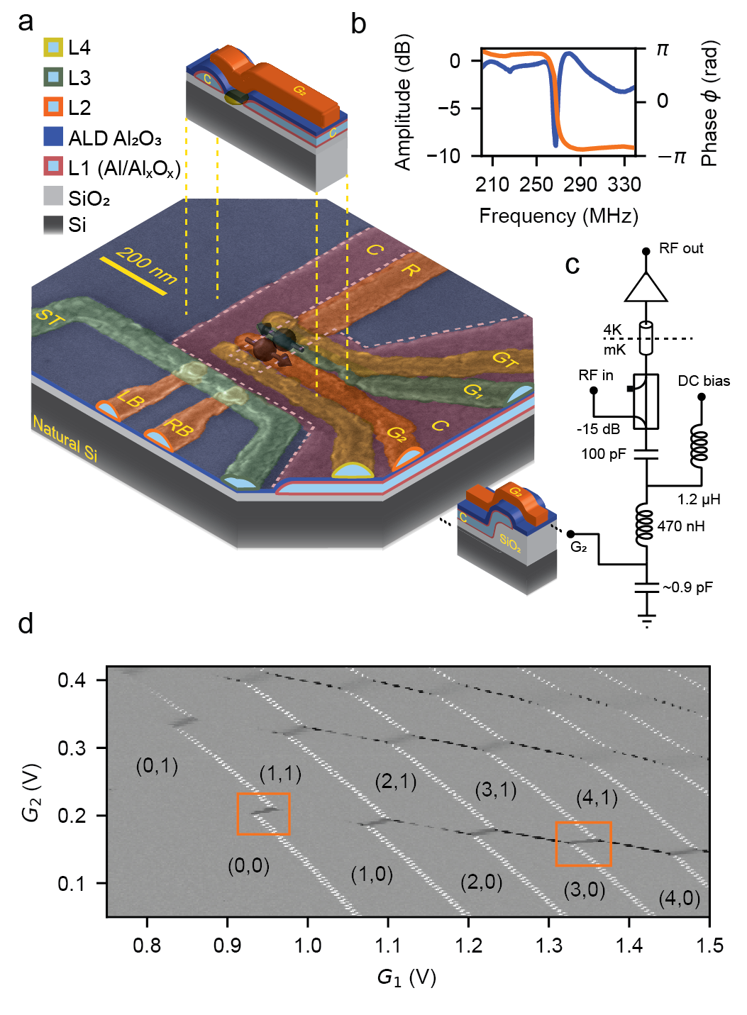
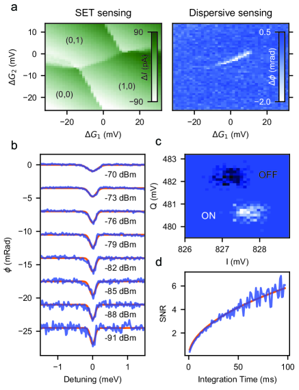
The charge stability diagram of a double quantum dot defined under gates and is shown in Figure 1d. We study the dispersive response at the to inter-dot transition (Fig 2a). While the SET is sensitive to any change in local charge density, the gate-based sensing only detects charge tunnelling that can follow the dispersive sensing frequency . The dot-to-reservoir transitions are not visible in the phase response due the slow (order kHz) tunnelling rates. At the location of the inter-dot charge transition, we observe a phase shift mrad (Fig. 2a, right), caused by the added quantum capacitance of the electron tunnelling between the dotsPetersson2010Charge ; Cottet2011Mesoscopic ; mizuta_quantum_2017 , where is the energy detuning between the dot chemical potentials, is the lever-arm relating the voltage on to detuning, , and the ground state energy dispersion for tunnel coupled dots. When the rf probe power is sufficiently low (Fig. 2b) the intrinsic width of the charge-transition is set by , yielding GHz (error margin here and elsewhere correspond to one standard deviation). From magneto-spectroscopy we find eV/V, which allows us to estimate an expected phase shift mrad, consistent with the measured response. The minimum integration time necessary to detect the phase shift is set by the effective noise temperature of the rf detection path and is limited by the noise temperature of the first amplifier. We extract a signal-to-noise ratio by comparing the change in the rf quadrature components due to the inter-dot tunnelling at with the variance obtained from repeated sampling (Fig. 2c, see Methods for details). For an integration time ms, we can detect single electron tunnelling with a SNR of 2 (Fig. 2d).
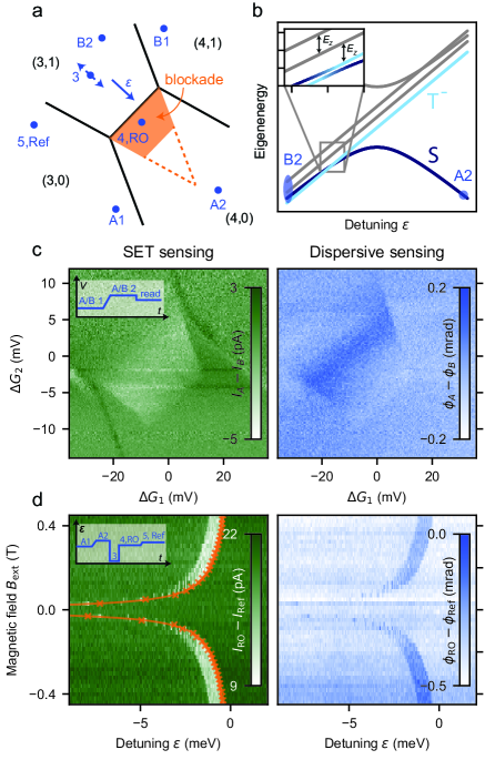
Having established and characterised the gate-based detection of single electron tunnelling, we now focus on the spin-readout capability. When a double quantum dot is occupied by two electrons, the Pauli exclusion principle prevents inter-dot tunnelling for all but the singlet spin state. This provides a means to probe the spin configuration via the change in gate-impedance near the inter-dot charge transition. In silicon, the valley degree of freedom acts as a low-lying orbital state that can break the spin blockade, as triplets can populate the excited valley state in a doubly occupied dot. Here we operate at the - inter-dot charge transition to avoid the low-lying valley state (estimated valley splitting µeV) which would otherwise serve to lift the spin blockade. At the - transition, two electrons in a spin-singlet state always fill the lower valley of dot 1, and do not affect the tunnel dynamics of the remaining two electrons. In Figure 3c, we compare the SET current and dispersive response for two different state initialisation protocolsFogarty2017Integrated (/ and /, Fig. 3a,b). For protocol , plunging into from () initialises a spin-singlet state due to the large energy gap to the first excited triplet state. The singlet initialisation is confirmed by the detection of a dispersively detected phase shift near the inter-dot transition (See Supplementary Figure S2). Conversely, for protocol , at low external magnetic field (for the data in Fig. 3c and Fig. 4 we set mT , with the electron gyromagnetic ratio and the electron temperature of the reservoir), unloading an electron by pulsing into from (), randomises the spin state into a mixture of singlet and triplets. The resulting partial blockade of tunnelling can be observed when subtracting the signals obtained from initialisation protocols and (Fig. 3c), and shows the expected Pauli spin blockade triangle (cut off by the first available triplet-like state of dot 1 at meV, attributed to the first orbital excited state). We further verify the spin nature of the blockade by probing the coupling between the hybridised singlet state and the lowest triplet spin state (Fig. 3b). The anti-crossing was previously studied in this systemFogarty2017Integrated ; Tanttu2018Controlling , and is mediated here by a combination of hyperfine and spin-orbit interaction. After -initialisation (protocol ), we plunge into along the detuning axis (3) shown in Fig. 3a and vary plunge depth and external magnetic field . When corresponds to the location of the anti-crossing, we expect a reduced singlet return probability, resulting in Pauli spin blockade signal at the readout point (4,RO). and recorded at a reference point (5,Ref) in are subtracted to counter slow drifts. We observe a characteristic spin-funnelPetta2005Coherent via both SET and phase response, mapping out location of the anti-crossing (Fig. 3d). Based on a Hamiltonian modelFogarty2017Integrated , the shape of the funnel determines the tunnel coupling at this inter-dot transition, GHz, consistent with the observed phase-shift.
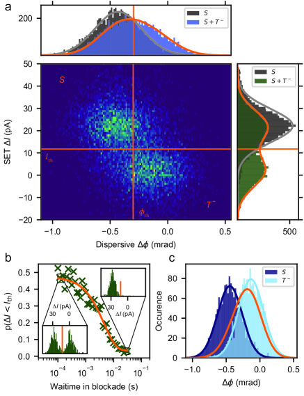
To estimate the spin-readout signal one can obtain in a single shot (for a single preparation of the qubit), we make a histogram of single-shot experiments (Fig. 4a), where a slow pulse to the crossing is used to initialise an evenly mixed state (for reference a -initialised state, using only initialisation protocol , is also shown in grey in the marginal distributions, Fig. 4a, top and right). The single-shot measurements show a bi-modal distribution, with a clear correlation between the SET current and dispersively detected phase-shift. This allows us to estimate the spin readout fidelity, using a modelBarthel2009Rapid for singlet-triplet readout to fit the marginal distributions for the and initialised states (see Methods for details). The model takes into account the finite triplet blockade lifetime ms and the initialisation fraction (), determined from an independent measurement presented in Figure 4b. We first fit the SET and dispersive readout distributions independently (Fig. 4a, top and right, solid lines show the resulting model output). Performing the fit for various integration times and choosing an optimal threshold yields the average - readout fidelity . We find % for an optimal ms. Similarly, for the dispersive readout, % for ms. Then, as a cross-check, we use the SET readout to bin single shot events into clear or outcomes (Methods). From the overlap of the resulting dispersive readout histograms (Fig. 4c), and again taking into account , we obtain % for ms. We note that the Pauli spin blockade based readout used here is directly applicable to realise local parity measurements for error detection in arrays of single-spin based qubitsVeldhorst2017Silicon ; Jones2018Logical .
Although here the SET outperforms the dispersive gate-based sensing, modest improvements to the resonator circuit should significantly boost the gate-based readout fidelity. For example, superconducting spiral inductor-based resonators have been shown to attain quality factors exceeding 100, with typical parasitic capacitance values around 0.3 pFColless2013Dispersive ; Hornibrook2014Frequency . This would increase the observed phase shift eight-fold, resulting in an average gate-based spin readout fidelity exceeding 99% (Methods). Further improvements can be obtained using optimised external matching techniquesahmed_radio-frequency_2018 or parametric amplification. Moreover, we emphasise that even if an on-chip electrometer outperforms a gate-based solution in terms of readout sensitivity, its benefits must be weighed against the added complexity as the number of qubits is increased. Finally, the gate-based sensing naturally allows frequency multiplexing by operating resonant circuits with varying inductor values on each gateHornibrook2014Frequency .
In summary, we have characterised a gate-based approach for spin-qubit measurements in a future silicon quantum processor.The signal-to-noise ratio obtained with a simple resonant circuit is sufficient to read out the electronic spin state in a single shot. Our results, together with contemporaneous results in several other silicon quantum dot architecturesVandersypen2018Results ; pakkiam_single-shot_2018 ; urdampilleta_gate-based_2018 , open a path to the readout of many spin qubits in parallel, using a compact gate design that will be needed for large-scale quantum processors of the future.
.1 Methods
.1.1 Experimental methods
The device was fabricated on natural silicon using multi-level gate-stack MOS technologyVeldhorst2014addressable . Four layers of gates with thickness 25, 45, 65, and 65 nm were fabricated on top of 5.9 nm thick thermally grown using electron beam lithography and aluminium evaporation and separated by thermally grown aluminium-oxide. After the first layer was completed, we performed 50 cycles of atomic layer deposition at 275°C (intended thickness 6 nm), to grow an additional insulating film of between gate layers 1 and 2 (see Figure 1a). The device was bonded to a printed circuit board (PCB) in a copper enclosure and cooled down in a dilution refrigerator with electron base temperature of 180 mK. Ceramic chip inductors (Coilcraft 1206CS-471 and 1206CS-122) and capacitor were surface mounted on the PCB holding the device, to provide the resonant circuit and DC bias (see Figure 1b). rf reflectometry measurements were performed employing either a vector network analyser (Keysight Fieldfox, for the data in Fig. 1c) or a demodulation setup using a rf source (Stanford Research Systems SG380) and IQ demodulator (Polyphase AD0105). The rf detection path consisted of a directional coupler (Mini-Circuits ZEDC-15-2B), cryogenic amplifier (Miteq AFS3-00100200-10-CR-4) mounted to the 4K plate and two room temperature amplifiers (Mini-Circuits ZFL-1000LN+). The demodulated signal was further amplified and filtered at 100 kHz, 48 dB/octave (Stanford Research Systems SIM910 and SIM965) before digitisation at 200 kS/s (Gage Octopus CS8389). Charge stability diagrams were obtained using a double lock-in technique with dynamic voltage compensation. In order to estimate the signal-to-noise ratio for the detection of inter-dot tunnelling, we repeatedly sample the reflected rf quadratures at , () and far-detuned from the interdot transition (, keeping the same voltage on in order to avoid effects from changes in , see Supplementary Figure S1). We define the displacement signal power , where denotes the mean over the repeated samples. Similarly, we define the noise power , where denotes the standard deviation of the repeated samples. The SNR is .
.1.2 Single-shot readout fidelity analysis
Using the model by Barthel et al.Barthel2009Rapid , we describe the single-shot readout histograms for the SET and dispersive response by . For the SET readout, we replace by the SET current in above equation, while for dispersive readout we replace by phase shift . is the initialisation fraction, is the total number of single shot readout events, is the histogram bin-size, , and , with the integration time and the blockade lifetime. To fit the model to the measured histograms, we proceed as follows: first we use the singlet initialised data (grey histograms in Fig. 4a) to determine (fixing ). Then, the + initialised histogram is fit to obtain and , where ms and are fixed to the values obtained from the data in Figure 4b. , and are independently fit for the SET and dispersive readout. This procedure is repeated for increasing integration time , and for each integration time the optimal threshold is chosen that maximises the average readout fidelity , with , (for the case , the integration boundaries are inverted). The resulting readout fidelities are shown in Supplementary Figure S3 (green and blue lines). The data in Figure 4c is obtained by using the SET signal to categorise single-shot events that have a clear or result: we categorise single-shot readout events that have as readout events, and as readout events. Here, pA, pA, where pA is the optimal single-shot readout threshold for the SET at time ms. We fit a single Gaussian to each of the and categorised event histograms (varying ) to obtain an accurate value for and respectively, as well as . Inserting these values (and ) in the model above is sufficient to calculate , choosing the optimal for each (orange line in Supplementary Figure S3).
To estimate the readout fidelity that could be obtained for improved parasitic capacitance and resonator quality factor , we use , which for the values given in the main text gives a factor 7.8 increase in compared to current values. Setting in the model above (assuming unchanged) gives .
.2 Acknowledgements
We thank M. House and A. Laucht for helpful discussions and C. Escott for valuable feedback on the manuscript. We acknowledge support from the US Army Research Office (W911NF-17-1-0198), the Australian Research Council (CE11E0001017), and the NSW Node of the Australian National Fabrication Facility. The views and conclusions contained in this document are those of the authors and should not be interpreted as representing the official policies, either expressed or implied, of the Army Research Office or the U.S. Government. The U.S. Government is authorised to reproduce and distribute reprints for Government purposes notwithstanding any copyright notation herein. M.F.G.Z. is supported by the Horizon 2020 programme through Grant Agreement No. 688539. B.H. acknowledges support from the Netherlands Organisation for Scientific Research (NWO) through a Rubicon Grant. This work was partly supported by the Winton Fund for the Physics of Sustainability.
.3 Author contributions
A.W., B.H. and A.J. performed the experiments. A.W. designed the device with input from A.R. and M.F.G., A.W. and F.E.H. fabricated the device with A.S.D’s supervision. T.T., C.H.Y. and A.M. contributed to the preparation of experiments and experimental systems. A.R. and M.F.G supervised early experiments. A.W., B.H. and A.J. designed the experiments under the supervision of A.S.D., with D.R. contributing to results discussion and interpretation. B.H. and A.W. wrote the manuscript with input from all co-authors.
References
- (1) Veldhorst, M. et al. An addressable quantum dot qubit with fault-tolerant control-fidelity. Nature Nanotechnology 9, 981–985 (2014).
- (2) Kawakami, E. et al. Electrical control of a long-lived spin qubit in a Si/SiGe quantum dot. Nature Nanotechnology 9, 666–670 (2014).
- (3) Veldhorst, M. et al. A two-qubit logic gate in silicon. Nature 526, 410–414 (2015).
- (4) Maurand, R. et al. A CMOS silicon spin qubit. Nature Communications 7, 13575 (2016).
- (5) Zajac, D., Hazard, T., Mi, X., Nielsen, E. & Petta, J. Scalable Gate Architecture for a One-Dimensional Array of Semiconductor Spin Qubits. Physical Review Applied 6, 054013 (2016).
- (6) Watson, T. F. et al. A programmable two-qubit quantum processor in silicon. Nature 555, 633–637 (2018).
- (7) Zajac, D. M. et al. Resonantly driven CNOT gate for electron spins. Science 359, 439–442 (2018).
- (8) Huang, W. et al. Fidelity benchmarks for two-qubit gates in silicon. arXiv:1805.05027 [cond-mat, physics:quant-ph] (2018).
- (9) Petersson, K. D. et al. Charge and Spin State Readout of a Double Quantum Dot Coupled to a Resonator. Nano Letters 10, 2789–2793 (2010).
- (10) House, M. G. et al. Radio frequency measurements of tunnel couplings and singlet–triplet spin states in Si:P quantum dots. Nature Communications 6, 8848 (2015).
- (11) Betz, A. C. et al. Dispersively Detected Pauli Spin-Blockade in a Silicon Nanowire Field-Effect Transistor. Nano Letters 15, 4622–4627 (2015).
- (12) Colless, J. I. et al. Dispersive Readout of a Few-Electron Double Quantum Dot with Fast rf Gate Sensors. Physical Review Letters 110, 046805 (2013).
- (13) Gonzalez-Zalba, M. F., Barraud, S., Ferguson, A. J. & Betz, A. C. Probing the limits of gate-based charge sensing. Nature Communications 6 (2015).
- (14) Rossi, A., Zhao, R., Dzurak, A. S. & Gonzalez-Zalba, M. F. Dispersive readout of a silicon quantum dot with an accumulation-mode gate sensor. Applied Physics Letters 110, 212101 (2017).
- (15) Ahmed, I. et al. Radio-Frequency Capacitive Gate-Based Sensing. Phys. Rev. Applied 10, 014018 (2018).
- (16) Petta, J. R. et al. Coherent Manipulation of Coupled Electron Spins in Semiconductor Quantum Dots. Science 309, 2180–2184 (2005).
- (17) Barthel, C., Reilly, D. J., Marcus, C. M., Hanson, M. P. & Gossard, A. C. Rapid Single-Shot Measurement of a Singlet-Triplet Qubit. Physical Review Letters 103, 160503 (2009).
- (18) Elzerman, J. M. et al. Single-shot read-out of an individual electron spin in a quantum dot. Nature 430, 431–435 (2004).
- (19) Nielsen, M. A. & Chuang, I. L. Quantum Computation and Quantum Information (Cambridge University Press, 2004), 1 edn.
- (20) Jones, C. et al. Logical Qubit in a Linear Array of Semiconductor Quantum Dots. Physical Review X 8, 021058 (2018).
- (21) Hill, C. D. et al. A surface code quantum computer in silicon. Science Advances 1, e1500707 (2015).
- (22) Veldhorst, M., Eenink, H. G. J., Yang, C. H. & Dzurak, A. S. Silicon CMOS architecture for a spin-based quantum computer. Nature Communications 8, 1766 (2017).
- (23) Vandersypen, L. M. K. et al. Interfacing spin qubits in quantum dots and donors—hot, dense, and coherent. npj Quantum Information 3, 34 (2017).
- (24) Li, R. et al. A crossbar network for silicon quantum dot qubits. Science Advances 4, eaar3960 (2018).
- (25) Tanttu, T. et al. Controlling spin-orbit interactions in silicon quantum dots using magnetic field direction. arXiv:1807.10415 [cond-mat] (2018).
- (26) Croot, X. G. et al. Gate-Sensing Charge Pockets in the Semiconductor Qubit Environment. arXiv:1706.09626 [cond-mat] (2017).
- (27) Cottet, A., Mora, C. & Kontos, T. Mesoscopic admittance of a double quantum dot. Physical Review B 83, 121311 (2011).
- (28) Mizuta, R., Otxoa, R. M., Betz, A. C. & Gonzalez-Zalba, M. F. Quantum and tunneling capacitance in charge and spin qubits. Phys. Rev. B 95, 045414 (2017).
- (29) Fogarty, M. A. et al. Integrated silicon qubit platform with single-spin addressability, exchange control and robust single-shot singlet-triplet readout. arXiv:1708.03445 [quant-ph] (2017).
- (30) Hornibrook, J. M. et al. Frequency multiplexing for readout of spin qubits. Applied Physics Letters 104, 103108 (2014).
- (31) Vandersypen, L. & group. Private communication (2018).
- (32) Pakkiam, P. et al. Single-shot single-gate RF spin readout in silicon. arXiv:1809.01802 [cond-mat, physics:quant-ph] (2018).
- (33) Urdampilleta, M. et al. Gate-Based High Fidelity Spin Read-out in a CMOS Device. arXiv:1809.04584 [cond-mat] (2018).