Spin-Orbit Protection of Induced Superconductivity in Majorana Nanowires
Abstract
Spin-orbit interaction (SOI) plays a key role in creating Majorana zero modes in semiconductor nanowires proximity coupled to a superconductor. We track the evolution of the induced superconducting gap in InSb nanowires coupled to a NbTiN superconductor in a large range of magnetic field strengths and orientations. Based on realistic simulations of our devices, we reveal SOI with a strength of 0.15–0.35 eVÅ. Our approach identifies the direction of the spin-orbit field, which is strongly affected by the superconductor geometry and electrostatic gates.
Spin-orbit interaction (SOI) is a relativistic effect that results from electrons moving (orbit) in an electric field () experiencing a magnetic field () in their moving reference frame that couples to the electron’s magnetic moment (spin). SOI is an essential ingredient of various realizations of topological superconductors, which host Majorana zero modes, the building blocks of topological quantum computation Kitaev (2001); Fu and Kane (2008); Nayak et al. (2008). The prime platform for topological quantum computation is based on a semiconductor nanowire coupled to a superconductor, where the proximity effect opens a superconducting energy gap in the density of states of the nanowire Lutchyn et al. (2010); Oreg et al. (2010). In general, a magnetic field suppresses superconductivity by closing the superconducting gap due to Zeeman and orbital effects Nijholt and Akhmerov (2016). If the nanowire has strong SOI, suppression of the superconducting gap is counteracted and a sufficiently large Zeeman energy drives the system into a topological superconducting phase, with Majorana zero modes localized at the wire ends Lutchyn et al. (2010); Oreg et al. (2010). The main experimental effort in the last few years has focused on detecting these Majorana zero modes as a zero-bias peak in the tunneling conductance Mourik et al. (2012); Albrecht et al. (2016); Deng et al. (2016); Gül et al. (2018); Zhang et al. (2018); Lutchyn et al. (2018); Aguado (2017). However, SOI, the mechanism providing the topological protection, has been challenging to detect directly in Majorana nanowires.
The electric field that gives rise to SOI in our system mainly results from structural inversion asymmetry of the confinement potential (Rashba SOI), which depends on the work function difference at the interface between the nanowire and the superconductor and on voltages applied to nearby electrostatic gates Vuik et al. (2016); Antipov et al. (2018); Woods et al. (2018); Mikkelsen et al. (2018). The Rashba SOI in nanowires has been investigated extensively by measuring spin-orbit related quantum effects: level repulsion of quantum dot levels Fasth et al. (2007); Nadj-Perge et al. (2012), and of Andreev states de Moor et al. (2018); Deng et al. (2016), weak antilocalization in long diffusive wires Hansen et al. (2005); van Weperen et al. (2015), and a helical liquid signature in short quasiballistic wires Kammhuber et al. (2017).
However, the SOI strength relevant to the topological protection is affected by the presence of the superconductor, necessitating direct observation of SOI in Majorana nanowires. Here, we reveal SOI in an InSb nanowire coupled to a NbTiN superconductor through the dependence of the superconducting gap on the magnetic field, both strength and orientation. We find that the geometry of the superconductor on the nanowire strongly modifies the direction of the spin-orbit field, which is further tunable by electrostatic gating, in line with the expected modifications of the electric field due to work function difference and electrostatic screening at the nanowire-superconductor interface.
Figure 1(a) shows the device image. An InSb nanowire (blue) is covered by a NbTi/NbTiN superconducting contact (purple) and a Cr/Au normal metal contact (yellow). The barrier gate underneath the uncovered wire (red) can deplete the nanowire, locally creating a tunnel barrier. The tunneling differential conductance () resolves the induced superconducting gap, by sweeping the bias voltage () across the tunnel barrier [Fig. 1(b)]. The dashed arrow indicates the induced gap of 0.65 meV. In this device, we have recently shown ballistic transport and Majorana signatures Gül et al. (2018).
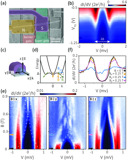
The magnetic field () dependence of the induced gap of device , with along three different directions, is shown in Fig. 1(e). The coordinate system is illustrated in Fig. 1(c). The axis is along the nanowire, parallel to the electron momentum (). The axis is perpendicular to the substrate and coincides with the electric field () direction due to the spatial symmetry of the device and the bottom gate. Since the Rashba spin-orbit field ( ) is perpendicular to both and , it points along the axis. When is aligned with or [left and right panels in Fig. 1(e)], both perpendicular to , the gap closes slowly (at around 0.6 T), followed by the emergence of a zero-bias peak possibly characteristic of a Majorana zero mode when is along the nanowire, although we emphasize that a conjecture of Majorana zero modes is not essential for the purposes of this Letter. On the contrary, when is aligned with the axis (middle panel), parallel to , the gap closes much faster (at around 0.25 T). Figure 1f shows the line cuts at 0.25 T along the three axes: for , the gap is almost the same as when 0 T, while the gap is closed for . This observation matches the predictions of the Majorana nanowire model, as illustrated in Fig. 1(d): when , SOI counteracts the Zeeman-induced gap closing by rotating the spin eigenstate towards , which reduces the component of the Zeeman field along the direction of the spin eigenstate. In contrast, when , the spin eigenstate is always parallel to , which prevents spin-orbit protection and results in a fast gap closing Osca et al. (2014); Rex and Sudbø (2014). This pronounced anisotropy of the gap closing with respect to different directions is universally observed in over ten devices (four shown in this Letter) for all gate settings
111See Supplemental Material, which includes Refs.
Car et al. (2014); Flöhr et al. (2011); Suyatin et al. (2007); Gül et al. (2017); Liu et al. (2017); Danon et al. (2017); Hofstadter (1976); Gropp et al. (1996); Du and Wu (1999); Prada et al. (2012); Pientka et al. (2012); Stanescu et al. (2012), for experimental details, theoretical details, and additional experimental data, which is a direct consequence of SOI in Majorana nanowires.
Before we discuss the SOI in more detail, we rule out alternative mechanisms for the anisotropy which can originate in the bulk superconductor, or the InSb nanowire. First, an anisotropic magnetic field-induced closing of the bulk superconducting gap is excluded for the fields we apply, which are far below the critical field of NbTiN (9 T) Van Woerkom et al. (2015). We note that this is different from aluminium films Chang et al. (2015); Deng et al. (2016); Gazibegovic et al. (2017); Zhang et al. (2018), where a small magnetic field (0.3 T) perpendicular to the film completely suppresses superconductivity, making them unsuitable to reveal SOI from an anisotropic gap closing. Next, we consider Meissner screening currents in NbTiN that can cause deviations in the magnetic field in the nanowire. Our Ginzburg-Landau simulations show that the field corrections due to Meissner screening are negligible Note (1), since the dimensions of the NbTiN film (1 m) are comparable to the penetration depth (290 nm). The simulations also show that vortex formation is most favorable along the axis Note (1), which implies that the observed anisotropic gap closing is not caused by gap suppression due to vortices near the nanowire Takei et al. (2013), since we do not observe the fastest gap closing along [Fig. 1(f)]. Finally, in the InSb nanowire, the Zeeman factor can become anisotropic due to quantum confinement Nadj-Perge et al. (2012); Pryor and Flatté (2006); Qu et al. (2016). However, our nanowire geometry leads to confinement in both the and directions, implying similar gap closing along and , inconsistent with our observations [Fig. 1(e)].
Having excluded the above mechanisms, we are now left with three effects: spin splitting of the electron states in magnetic fields with the Landé factor (Zeeman effect), the orbital effect of the magnetic field representing the Lorentz force acting on traveling electrons, and SOI. To investigate the role of these effects, we use a theoretical three-dimensional Majorana nanowire model defined by the Hamiltonian Lutchyn et al. (2010); Oreg et al. (2010); Nijholt and Akhmerov (2016):
Here, the first term represents the kinetic and potential energy, with the chemical potential measured from the middle of the helical gap and is the electrostatic potential in the wire, whose magnitude is parametrized by , with the direction of the electric field and the wire radius. The orbital effect enters the Hamiltonian via the vector potential in the canonical momentum: . Here, is the electron charge, is Plank’s constant, and 0.015 is the effective mass with the electron mass. The second term represents Rashba SOI characterized by a SOI strength , which we set to 0.2 eVÅ to find qualitative agreement with the measurements. The third term is the Zeeman term, with an isotropic factor set to 50 and is the Bohr magneton. The last term accounts for the superconducting proximity effect, which we implement in the weak coupling approximation Nijholt and Akhmerov (2016). The Pauli matrices and act in the particle-hole and spin space respectively. We perform numerical simulations of this Hamiltonian on a 3D lattice in a realistic nanowire geometry using the kwant code Groth et al. (2014). We note that recent theory work shows that the anisotropy is unaffected by additional factors such as the wire length, temperature, and strong coupling to the superconductor Liu et al. (2019). Additional details are provided in the Supplemental Material Note (1).
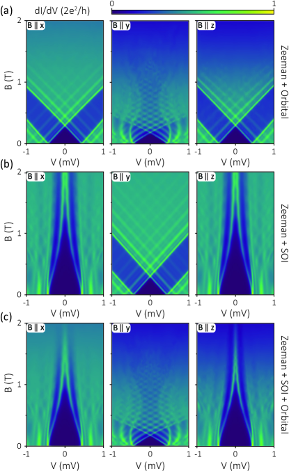
We identify which effects explain the observed anisotropic gap closing behavior by including them separately in our simulations. Figure 2(a) shows the magnetic field dependence of the gap without SOI (setting 0 in the Hamiltonian). In contrast to Fig. 1(e) the gap closes around 0.3 T for all three directions, reflecting the dominant contribution of the Zeeman effect. In Fig. 2(b), we turn on the SOI, and turn off the orbital effect by setting the magnetic vector potential 0, which qualitatively reproduces the anisotropic behavior between the axis and the and -axes. We have explored other combinations of parameters and find that the experimental results of Fig. 1(e) can only be reproduced by including SOI. We note that adding the orbital effect in Fig. 2(c) shifts the gap closing to a field almost twice as small for , which explains why we observe a gap closing for at around 0.25 T, far below 0.45 T, the critical field expected when only the Zeeman effect with 50 suppresses the gap. By fitting the curvature of the gap closing van Heck et al. (2017); Pan et al. (2019) along [white dashed line in Fig. 1(e)] we estimate a range of the SOI strength of 0.15 – 0.35 eVÅ from devices - (for fitting details and fits to additional devices, see Supplemental Material Note (1)). This SOI strength is in agreement with the values extracted from level repulsion of Andreev states Stanescu et al. (2013); de Moor et al. (2018) in an additional device Note (1). Since depends on the electric field in the wire, we expect the observed variation in the SOI strength of devices to be caused by differences in the applied gate voltages and wire diameter. Recently, the level repulsion of Andreev states in InSb nanowires covered with epitaxial aluminium has shown a SOI strength of approximately 0.1 eVÅde Moor et al. (2018), slightly lower than we find for NbTiN covered nanowires, most likely due to strong coupling to the aluminium superconductor, leading to stronger renormalization of the InSb material parameters Stanescu et al. (2011); Cole et al. (2015); Antipov et al. (2018); Woods et al. (2018); Mikkelsen et al. (2018); Reeg et al. (2018).
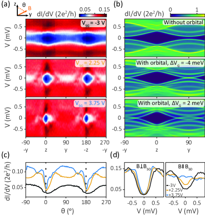
To resolve the direction of the spin-orbit field, we fix the amplitude and continuously rotate the direction, parametrized by the angle in the plane [inset Fig. 3(a)]. Figure 3(a) shows the dependence of the gap on , where we adjust the electric field strength in the nanowire with a voltage on the super gate (SG) underneath the superconductor [green in Fig. 1(a)]. We define the angle at which the gap is hardest as and find 3 ( axis) for all and in multiple devices (Fig. 3 and Fig. S5 Note (1)) (error due to uncertainty in the extraction procedure). This is illustrated in Fig. 3(c), which shows horizontal line cuts for subgap bias. The largest gap for a given amplitude is expected for , indicating that , in agreement with the -field direction dictated by the device geometry.
Now, we check whether the orbital effect changes . The simulations in Fig. 3(b) show the effect of magnetic field rotation on the gap with , confirming that is, indeed, always given by the direction perpendicular to , i.e. . Comparing the top panel (without the orbital effect) with the middle panel (with the orbital effect), we conclude that the orbital effect does not affect . This conclusion also holds when we vary the potential difference between the middle and outer of the wire (corresponding to ) in the middle panel and bottom panel. We note that, at 2 meV (bottom panel) the wave function is moved towards the bottom of the nanowire, which increases the strength of the orbital effect by breaking the reflection symmetry about the axis, as evidenced by the longer angle range over which the gap is closed compared to -4 meV (middle panel). Experimentally, we also observe this in Fig. 3(a), with line cuts in Fig. 3(c), where the gap is closed over a significantly longer angle range with increasing . We note that we use small values of in the simulations, because we expect a weak gate response due to effective electrostatic screening by the superconductor, which covers five of the six nanowire facets Zhang et al. (2017).
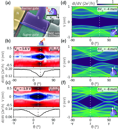
Finally, we turn to a second type of device in which the superconducting film only partially covers the nanowire facets [Fig. 4(a)]. This partial superconductor coverage can modify the orientation of by changing the associated electric field direction Vuik et al. (2016), as sketched in the inset of Fig. 4(a). The electric field in the wire has two main origins. The first one originates from the work function difference between the superconductor and nanowire, which leads to charge redistribution. The resulting electric field is expected to rotate away from the axis due to the partial superconductor coverage which breaks the spatial symmetry. In Fig. 4(b) we rotate in the plane, perpendicular to the nanowire axis, and find that is, indeed, no longer at zero, but at 32 . The second contribution to the electric field arises from the applied and the electrostatic screening due to the grounded superconductor. Changing should, therefore, rotate the electric field for partial coverage. Indeed, we find that shifts by by adjusting by 7.5 V [Fig. 4(c)]. Field rotation at intermediate and magnetic field sweeps confirming the change of are shown in the Supplemental Material Note (1). Our theory simulations confirm that is still given by the direction orthogonal to when the electric field is not necessarily along a spatial symmetry axis of the partially covered device [Fig. 4(d) and 4(e)]. While the orbital effect does not change [Fig. 4(e) and 4(f)], it can induce asymmetry in the energy spectrum around resulting from wave function asymmetry when the electric field is not along the mirror plane of the device [Fig. 4(b) and Fig. 4(e)]. The significance of the orbital effect in our devices underlines the importance of including it in realistic simulations of Majorana nanowires.
In conclusion, the observed gap closing anisotropy for different magnetic field orientations demonstrates SOI in our Majorana nanowires, a necessary condition to create Majorana zero modes. Our experiments reveal that SOI is strongly affected by the work function difference at the nanowire-superconductor interface and the geometry of the superconductor, while electrostatic gating provides tunability of SOI.
Acknowledgements.
We thank O.W.B. Benningshof, A. Geresdi, S. Goswami, M.W.A. de Moor, M. Quintero-Pérez and P. Rożek for valuable feedback and assistance. This work has been supported by the Netherlands Organization for Scientific Research (NWO), Foundation for Fundamental Research on Matter (FOM), European Research Council (ERC) and Microsoft Corporation Station Q. The work of F.N.R. and E.B. was supported by the Swedish Research Council Grant No. 642-2013-7837 and by Göran Gustafsson Foundation for Research in Natural Sciences and Medicine. J.D.S.B., H.Z. and Ö.G. contributed equally to this work.References
- Kitaev (2001) A. Y. Kitaev, Unpaired Majorana fermions in quantum wires, Phys. Usp. 44, 131 (2001).
- Fu and Kane (2008) L. Fu and C. L. Kane, Superconducting proximity effect and Majorana fermions at the surface of a topological insulator, Phys. Rev. Lett. 100, 096407 (2008).
- Nayak et al. (2008) C. Nayak, S. H. Simon, A. Stern, M. Freedman, and S. Das Sarma, Non-Abelian anyons and topological quantum computation, Rev. Mod. Phys. 80, 1083 (2008).
- Lutchyn et al. (2010) R. M. Lutchyn, J. D. Sau, and S. Das Sarma, Majorana fermions and a topological phase transition in semiconductor-superconductor heterostructures, Phys. Rev. Lett. 105, 077001 (2010).
- Oreg et al. (2010) Y. Oreg, G. Refael, and F. von Oppen, Helical liquids and Majorana bound states in quantum wires, Phys. Rev. Lett. 105, 177002 (2010).
- Nijholt and Akhmerov (2016) B. Nijholt and A. R. Akhmerov, Orbital effect of magnetic field on the Majorana phase diagram, Phys. Rev. B 93, 235434 (2016).
- Mourik et al. (2012) V. Mourik, K. Zuo, S. M. Frolov, S. R. Plissard, E. P. A. M. Bakkers, and L. P. Kouwenhoven, Signatures of Majorana fermions in hybrid superconductor-semiconductor nanowire devices, Science 336, 1003 (2012).
- Albrecht et al. (2016) S. M. Albrecht, A. P. Higginbotham, M. Madsen, F. Kuemmeth, T. S. Jespersen, J. Nygård, P. Krogstrup, and C. M. Marcus, Exponential protection of zero modes in Majorana islands, Nature 531, 206 (2016).
- Deng et al. (2016) M. T. Deng, S. Vaitiekėnas, E. B. Hansen, J. Danon, M. Leijnse, K. Flensberg, J. Nygård, P. Krogstrup, and C. M. Marcus, Majorana bound state in a coupled quantum-dot hybrid-nanowire system, Science 354, 1557 (2016).
- Gül et al. (2018) Ö. Gül, H. Zhang, J. D. S. Bommer, M. W. A. De Moor, D. Car, S. R. Plissard, E. Bakkers, A. Geresdi, K. Watanabe, T. Taniguchi, and L. P. Kouwenhoven, Ballistic Majorana nanowire devices, Nat. Nanotech. 13, 192 (2018).
- Zhang et al. (2018) H. Zhang, C.-X. Liu, S. Gazibegovic, D. Xu, J. A. Logan, G. Wang, N. van Loo, J. D. S. Bommer, M. W. A. De Moor, D. Car, R. L. M. Op het Veld, P. J. van Veldhoven, S. Koelling, M. A. Verheijen, M. Pendharkar, D. J. Pennachio, B. Shojaei, J. S. Lee, C. J. Palmstrøm, E. P. A. M. Bakkers, S. D. Sarma, and L. P. Kouwenhoven, Quantized Majorana conductance, Nature 556, 74 (2018).
- Lutchyn et al. (2018) R. M. Lutchyn, E. P. A. M. Bakkers, L. P. Kouwenhoven, P. Krogstrup, C. M. Marcus, and Y. Oreg, Majorana zero modes in superconductor-semiconductor heterostructures, Nat. Rev. Mater. 3, 52 (2018).
- Aguado (2017) R. Aguado, Majorana quasiparticles in condensed matter, Riv. Nuovo Cimento 40, 523 (2017).
- Vuik et al. (2016) A. Vuik, D. Eeltink, A. R. Akhmerov, and M. Wimmer, Effects of the electrostatic environment on the Majorana nanowire devices, New J. Phys. 18, 033013 (2016).
- Antipov et al. (2018) A. E. Antipov, A. Bargerbos, G. W. Winkler, B. Bauer, E. Rossi, and R. M. Lutchyn, Effects of gate-induced electric fields on semiconductor majorana nanowires, Phys. Rev. X 8, 031041 (2018).
- Woods et al. (2018) B. D. Woods, T. D. Stanescu, and S. Das Sarma, Effective theory approach to the Schrödinger-Poisson problem in semiconductor Majorana devices, Phys. Rev. B 98, 035428 (2018).
- Mikkelsen et al. (2018) A. E. G. Mikkelsen, P. Kotetes, P. Krogstrup, and K. Flensberg, Hybridization at superconductor-semiconductor interfaces, Phys. Rev. X 8, 031040 (2018).
- Fasth et al. (2007) C. Fasth, A. Fuhrer, L. Samuelson, V. N. Golovach, and D. Loss, Direct measurement of the spin-orbit interaction in a two-electron InAs nanowire quantum dot, Phys. Rev. Lett. 98, 266801 (2007).
- Nadj-Perge et al. (2012) S. Nadj-Perge, V. S. Pribiag, J. W. G. van den Berg, K. Zuo, S. R. Plissard, E. P. A. M. Bakkers, S. M. Frolov, and L. P. Kouwenhoven, Spectroscopy of spin-orbit quantum bits in indium antimonide nanowires, Phys. Rev. Lett. 108, 166801 (2012).
- de Moor et al. (2018) M. W. A. de Moor, J. D. S. Bommer, D. Xu, G. W. Winkler, A. E. Antipov, A. Bargerbos, G. Wang, N. van Loo, R. L. M. O. het Veld, S. Gazibegovic, D. Car, J. A. Logan, M. Pendharkar, J. S. Lee, E. P. A. M. Bakkers, C. J. Palmstrøm, R. M. Lutchyn, L. P. Kouwenhoven, and H. Zhang, Electric field tunable superconductor-semiconductor coupling in majorana nanowires, New J. of Phys. 20, 103049 (2018).
- Hansen et al. (2005) A. E. Hansen, M. T. Björk, C. Fasth, C. Thelander, and L. Samuelson, Spin relaxation in InAs nanowires studied by tunable weak antilocalization, Phys. Rev. B 71, 205328 (2005).
- van Weperen et al. (2015) I. van Weperen, B. Tarasinski, D. Eeltink, V. S. Pribiag, S. R. Plissard, E. P. A. M. Bakkers, L. P. Kouwenhoven, and M. Wimmer, Spin-orbit interaction in InSb nanowires, Phys. Rev. B 91, 201413 (2015).
- Kammhuber et al. (2017) J. Kammhuber, M. C. Cassidy, F. Pei, M. P. Nowak, A. Vuik, O. Gül, D. Car, S. R. Plissard, E. P. A. M. Bakkers, M. Wimmer, and L. P. Kouwenhoven, Conductance through a helical state in an indium antimonide nanowire, Nat. Commun. 8, 478 (2017).
- Osca et al. (2014) J. Osca, D. Ruiz, and L. Serra, Effects of tilting the magnetic field in one-dimensional Majorana nanowires, Phys. Rev. B 89, 245405 (2014).
- Rex and Sudbø (2014) S. Rex and A. Sudbø, Tilting of the magnetic field in Majorana nanowires: Critical angle and zero-energy differential conductance, Phys. Rev. B 90, 115429 (2014).
- Note (1) See Supplemental Material, which includes Refs. Car et al. (2014); Flöhr et al. (2011); Suyatin et al. (2007); Gül et al. (2017); Liu et al. (2017); Danon et al. (2017); Hofstadter (1976); Gropp et al. (1996); Du and Wu (1999); Prada et al. (2012); Pientka et al. (2012); Stanescu et al. (2012), for experimental details, theoretical details, and additional experimental data.
- Car et al. (2014) D. Car, J. Wang, M. A. Verheijen, E. P. A. M. Bakkers, and S. R. Plissard, Rationally designed single-crystalline nanowire networks, Adv. Mater. 26, 4875 (2014).
- Flöhr et al. (2011) K. Flöhr, M. Liebmann, K. Sladek, H. Y. Günel, R. Frielinghaus, F. Haas, C. Meyer, H. Hardtdegen, T. Schäpers, D. Grützmacher, and M. Morgenstern, Manipulating InAs nanowires with submicrometer precision, Rev. Sci. Instrum. 82, 113705 (2011).
- Suyatin et al. (2007) D. B. Suyatin, C. Thelander, M. T. Björk, I. Maximov, and L. Samuelson, Sulfur passivation for ohmic contact formation to InAs nanowires, Nanotechnology 18, 105307 (2007).
- Gül et al. (2017) O. Gül, H. Zhang, F. K. de Vries, J. van Veen, K. Zuo, V. Mourik, S. Conesa-Boj, M. P. Nowak, D. J. van Woerkom, M. Quintero-Pérez, M. C. Cassidy, A. Geresdi, S. Koelling, D. Car, S. R. Plissard, E. P. A. M. Bakkers, and L. P. Kouwenhoven, Hard superconducting gap in InSb nanowires, Nano Lett. 17, 2690 (2017).
- Liu et al. (2017) C.-X. Liu, J. D. Sau, and S. Das Sarma, Role of dissipation in realistic Majorana nanowires, Phys. Rev. B 95, 054502 (2017).
- Danon et al. (2017) J. Danon, E. B. Hansen, and K. Flensberg, Conductance spectroscopy on Majorana wires and the inverse proximity effect, Phys. Rev. B 96, 125420 (2017).
- Hofstadter (1976) D. R. Hofstadter, Energy levels and wave functions of Bloch electrons in rational and irrational magnetic fields, Phys. Rev. B 14, 2239 (1976).
- Gropp et al. (1996) W. D. Gropp, H. G. Kaper, G. K. Leaf, D. M. Levine, M. Palumbo, and V. M. Vinokur, Numerical simulation of vortex dynamics in type-II superconductors, J. Comput. Phys. 123, 254 (1996).
- Du and Wu (1999) Q. Du and X. Wu, Numerical solution of the three-dimensional Ginzburg–Landau models using artificial boundary, SIAM J. Numer. Anal. 36, 1482 (1999).
- Prada et al. (2012) E. Prada, P. San-Jose, and R. Aguado, Transport spectroscopy of nanowire junctions with Majorana fermions, Phys. Rev. B 86, 180503 (2012).
- Pientka et al. (2012) F. Pientka, G. Kells, A. Romito, P. W. Brouwer, and F. von Oppen, Enhanced zero-bias Majorana peak in the differential tunneling conductance of disordered multisubband quantum-wire/superconductor junctions, Phys. Rev. Lett. 109, 227006 (2012).
- Stanescu et al. (2012) T. D. Stanescu, S. Tewari, J. D. Sau, and S. Das Sarma, To close or not to close: The fate of the superconducting gap across the topological quantum phase transition in Majorana-carrying semiconductor nanowires, Phys. Rev. Lett. 109, 266402 (2012).
- Van Woerkom et al. (2015) D. J. Van Woerkom, A. Geresdi, and L. P. Kouwenhoven, One minute parity lifetime of a NbTiN Cooper-pair transistor, Nat. Phys. 11, 547 (2015).
- Chang et al. (2015) W. Chang, S. M. Albrecht, T. S. Jespersen, F. Kuemmeth, P. Krogstrup, J. Nygård, and C. M. Marcus, Hard gap in epitaxial semiconductor-superconductor nanowires, Nat. Nanotech. 10, 232 (2015).
- Gazibegovic et al. (2017) S. Gazibegovic, D. Car, H. Zhang, S. C. Balk, J. A. Logan, M. W. A. De Moor, M. C. Cassidy, R. Schmits, D. Xu, G. Wang, P. Krogstrup, R. L. M. Op het Veld, K. Zuo, Y. Vos, J. Shen, D. Bouman, B. Shojaei, D. Pennachio, J. S. Lee, P. J. van Veldhoven, S. Koelling, M. A. Verheijen, L. P. Kouwenhoven, C. J. Palmstrøm, and E. P. A. M. Bakkers, Epitaxy of advanced nanowire quantum devices, Nature 548, 434 (2017).
- Takei et al. (2013) S. Takei, B. M. Fregoso, H.-Y. Hui, A. M. Lobos, and S. Das Sarma, Soft superconducting gap in semiconductor Majorana nanowires, Phys. Rev. Lett. 110, 186803 (2013).
- Pryor and Flatté (2006) C. E. Pryor and M. E. Flatté, Landé g factors and orbital momentum quenching in semiconductor quantum dots, Phys. Rev. Lett. 96, 026804 (2006).
- Qu et al. (2016) F. Qu, J. van Veen, F. K. de Vries, A. J. A. Beukman, M. Wimmer, W. Yi, A. A. Kiselev, B.-M. Nguyen, M. Sokolich, M. J. Manfra, F. Nichele, C. M. Marcus, and L. P. Kouwenhoven, Quantized conductance and large -factor anisotropy in InSb quantum point contacts, Nano Lett. 16, 7509 (2016).
- Groth et al. (2014) C. W. Groth, M. Wimmer, A. R. Akhmerov, and X. Waintal, Kwant: a software package for quantum transport, New J. Phys. 16, 063065 (2014).
- Liu et al. (2019) C.-X. Liu, J. D. Sau, T. D. Stanescu, and S. Das Sarma, Conductance smearing and anisotropic suppression of induced superconductivity in a Majorana nanowire, Phys. Rev. B 99, 024510 (2019).
- van Heck et al. (2017) B. van Heck, J. I. Väyrynen, and L. I. Glazman, Zeeman and spin-orbit effects in the Andreev spectra of nanowire junctions, Phys. Rev. B 96, 075404 (2017).
- Pan et al. (2019) H. Pan, J. D. Sau, T. D. Stanescu, and S. Das Sarma, Curvature of gap closing features and the extraction of Majorana nanowire parameters, Phys. Rev. B 99, 054507 (2019).
- Stanescu et al. (2013) T. D. Stanescu, R. M. Lutchyn, and S. Das Sarma, Dimensional crossover in spin-orbit-coupled semiconductor nanowires with induced superconducting pairing, Physical Rev. B 87, 094518 (2013).
- Stanescu et al. (2011) T. D. Stanescu, R. M. Lutchyn, and S. Das Sarma, Majorana fermions in semiconductor nanowires, Phys. Rev. B 84, 144522 (2011).
- Cole et al. (2015) W. S. Cole, S. Das Sarma, and T. D. Stanescu, Effects of large induced superconducting gap on semiconductor Majorana nanowires, Phys. Rev. B 92, 174511 (2015).
- Reeg et al. (2018) C. Reeg, D. Loss, and J. Klinovaja, Metallization of a Rashba wire by a superconducting layer in the strong-proximity regime, Phys. Rev. B 97, 165425 (2018).
- Zhang et al. (2017) H. Zhang, O. Gül, S. Conesa-Boj, M. P. Nowak, M. Wimmer, K. Zuo, V. Mourik, F. K. de Vries, J. van Veen, M. W. A. De Moor, J. D. S. Bommer, D. J. van Woerkom, D. Car, S. R. Plissard, E. P. A. M. Bakkers, M. Quintero-Pérez, M. C. Cassidy, S. Koelling, S. Goswami, K. Watanabe, T. Taniguchi, and L. P. Kouwenhoven, Ballistic superconductivity in semiconductor nanowires, Nat. Commun. 8, 16025 (2017).