Sign identification of electron and hole out-of-plane g factors
by utilizing nuclear spin switch in single quantum nanostructures
Abstract
The electron and hole g factors are the key quantities for the spin manipulations in semiconductor quantum nanostructures. However, for the individual nanostructures, the separate determination including the signs of those g factors is difficult by using some methods adopted conventionally in bulks and quantum wells. We report a convenient optical method for the sign identification of out-of-plane g factors in the individual quantum nanostructures, which utilizes the optically-induced nuclear spin switch. The method is demonstrated in typical single self-assembled In0.75Al0.25As/Al0.3Ga0.7As quantum dots and InAs/GaAs quantum rings, where the g factors with the opposite sign for electron and the same sign for hole are proved.
The carrier spin dynamics has always been one of the central topics in semiconductor spin physics OptOrientation ; SpinPhysics . In particular, the spin manipulations by electrical, magnetic and/or optical methods have been studied intensively SpinPhysics ; Slavcheva10 ; Bennett13 ; Nakaoka07 . One of the key quantities for the control protocols of localized carrier spins is the g factor, which is the coefficient connecting its magnetic dipole moment with the spin degrees of freedom. In general, the effective g factor in a semiconductor nanostructure deviates from the value dominantly determined by the material composition due to a wide variety of the modulations: for example, the spatial confinement in the nanostructures, the effect of strain-induced valence band mixing (VBM), and the penetration of the carrier wavefunction into the barrier material Snelling91 ; Sirenko97 ; Nakaoka04 ; Tholen16 .
Especially in semiconductor quantum nanostructures such as dots (QDs) and rings (QRs), some of such modulations are enhanced. The electron g factor is determined by a balance between the bare-electron contribution (+2.0) and a lattice orbital contribution, which may vary significantly in both magnitude and sign by strength of the confinement. Also, it has been found that the sign inversion of hole g factor is possible by the external means Bennett13 . The sign of g factor is obviously important because it dominates the energy diagram of target spins under the external and/or some effective magnetic fields, and consequently the signs of Zeeman splitting energy and spin precession direction. In order to realize composite spin rotations in a Bloch sphere by using magnetic fields, the sign of g factor determine the rotation direction and thus, the optimum shortest path in a Bloch sphere Slavcheva10 . Further, the direction of the photo-induced nuclear field also depends on the sign of g factor as shown later.
In the QD and QR structures, the electron and hole g factors gain another significant importance because the former is important to describe the dynamics of a coupled spin system with nuclei and the latter is essential to measure the VBM. This is because the hyperfine interaction (HFI) and VBM are enhanced for localized carriers due to the strong confinement and large residual strain compared to high dimensional structures like bulks and quantum wells (QWs). Since the effective g factors have the distribution even in the same sample, the individual measurement for target QDs is crucial.
Besides, several works have focused on developing techniques for the evaluation of electron and hole effective g factors (), and some methods to determine unambiguously the sign of have been demonstrated in QWs: the time-resolved photoluminescence (TR-PL) with the up-conversion technique Marie00 , TR-Kerr (or Faraday) rotation Malinowski00 ; Salis01 , and Hanle effect measurements Snelling91 ; Malinowski99 . In these methods, the external magnetic field is applied in the sample plane, and the optical axis of incident light is inclined with respect to the sample growth axis. The phase shift of the electron spin precession observed in the TR techniques and the peak shift of Hanle curve caused by an optically-induced nuclear field () are key points for the sign determination of . However, there are some problems to apply these methods to individual QDs and QRs; the TR measurements require relatively large number of electrons and is not successful in single self-assembled (SA) QDs. Although the Hanle effect measurement is possible for single QDs, the peak shift of Hanle curve is obscured by more prominent deformation “anomalous Hanle effect” due to the enhanced quadrupolar effect of nuclear spins Krebs10 ; Yamamoto18 . Further, if both the bright and dark exciton emissions appear under a longitudinal magnetic field, the electron and hole out-of-plane g factors (, ) can be deduced including their signs by using the standard time-integrated micro-PL (-PL) measurements. Although this method can be used for the (001)-oriented QDs with reduced symmetry in the shape Bayer99 ; Chekhovich10 and the (111)-oriented QDs Sallen11 , the selection of QDs is required. Therefore, the convenient method applicable for the standard single QDs is highly aspired.
In our previous work Kaji07 , we demonstrated the method to evaluate and separately by using the nuclear spin switch (NSSW) Tartakovskii07 . Although it was a powerful tool to know the magnitude of g factors, we got only the information of the sign of a product . In this paper, we demonstrate a useful method for separate evaluations of the signs of and as well as their magnitudes. The method utilizes the correlation of the NSSW and the sign of Zeeman splitting in the -PL measurements of single QDs. The method is demonstrated in typical single SA In0.75Al0.25As/Al0.3Ga0.7As QDs and InAs/GaAs QRs, and the observed g factors with the opposite sign for electron and the same sign for hole are proved. Since the electron and hole g factors in widely-used In(Ga)As and GaAs QDs have been studied experimentally and theoretically Nakaoka04 ; Bayer99 ; Sallen11 ; Kaji14 , the carrier g factors of InAlAs QDs, which have only a few reports, have to be investigated and compared by using an unified method.
We carried out the -PL measurements in the time-integrated mode at 6 K under a longitudinal magnetic field . A continuous wave Ti:sapphire laser was tuned to provide the transition energy to the foot of the wetting layer. The corresponding wavelengths were 730 nm for InAlAs QDs and 865 nm for InAs QRs. The excitation beam was focused on the sample surface using a microscope objective lens (20, NA0.4), and the PL signals were collected by the same objective lens and were detected by a triple-grating spectrometer and a liquid N2-cooled Si-CCD detector. The spectral resolution that determines the PL energies was 5 eV using the spectral fitting. The excitation light polarization was varied systematically by a set of a linear polarizer, a rotating half waveplate, and a quarter waveplate with a fixed angle ( rad.), and the polarization was monitored by a polarimeter.
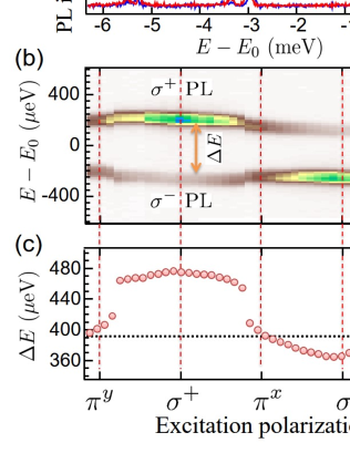
First, we show the results in InAlAs QDs following the sign identification method of the g factors. The SA-InAlAs/AlGaAs QDs grown on an undoped (100)-GaAs substrate by molecular beam epitaxy were used. The average diameter, height, and density of the QDs were found to be 20 nm, 4 nm, and 5 cm-2, respectively, by the atomic force microscopy measurements of a reference uncapped QD layer Yokoi05 . It is known that InAlAs/Al(Ga)As QDs have the complex band structure depending on the aluminum concentration and the QD size Debus14 . In the studied InAlAs QDs, the lowest electron level appears always in the valley, and the resultant direct gap structure gives a short recombination time of 1 ns to the QD exciton Kumano06 . Figure 1(a) shows the polarization-resolved PL spectra (, ) of a typical single InAlAs QD at 6 K and 0 T under the nonpolarized excitation. The spectra indicate the emissions of the neutral biexciton (), neutral exciton (), and positive trion () from the low energy side. Each charge state could be assigned by considering the fine structure splitting (FSS) and the binding energy Kaji_Thesis . The fact that these PL peaks originate from the same single QD can be confirmed with observing the response to the generated nuclear field by the circularly polarized excitation Sasakura08 .
Figure 1(b) shows a two-dimensional plot of the PL spectra as a function of the excitation polarization where the retardance of the excitation light is varied systematically under = T. The polarized PL peak appears at higher energy than the polarized one. The intensity and energy of each PL spectrum change clearly depending on the excitation polarization. Figure 1(c) indicates the change in energy splitting (). is defined as , where is the energy of the polarized PL peak. While decreases gradually and shows the minimum around the excitation, an abrupt increase of occurs by NSSW around the excitation. This change of by the generated nuclear field (Overhauser field) and the connection to the sign of the g factors will be explained later by using Fig. 2. Note that stabilizes enough within the exposure time of a CCD detector (1 s) because the formation time of the steady-state is 10 ms at the excitation condition.
Throughout this paper, we consider only the dipole-allowed transitions between the lowest electron states and the lowest mainly heavy-hole states . According to the selection rules of optical transitions, the polarization triggers the transition , and the polarization triggers the transition . Then, the sign of g factor is defined as follows; the positive (negative) sign of corresponds to the up-spin (down-spin) electron state in the higher energy side compared with the down-spin (up-spin) electron state under the positive . This definition comes from the standard relation between the magnetic moment and the electron spin : (: the Bohr magneton). In the case of the hole states, the down-spin (up-spin) hole state is in the higher energy side under according to the relation between the magnetic moment and spin of hole (positive charge), and then the sign is defined as () in this work comment . These definitions of polarization and the signs of and are indicated clearly in the state diagrams of Fig. 2(a) and (b).
In the demonstrated sign identification method of the g factors, we utilize the NSSW, which means the cancellation of by . In order to utilize the NSSW, the electron spin interacting with nuclear spins has to be defined; the optically-injected electron spin polarization is highly preserved after the relaxation to the lowest electron level of and in the measurements, which means that the electron and hole spin relaxation times are longer than the radiative recombination time. This condition can be realized generally even by the nonresonant excitation of the wetting layer as well as the resonant and quasi-resonant (e.g. 1LO) excitations. As a result, the same polarized PL peak as the excitation polarization has a larger intensity. In the case of , since the remained electron spin after the e-h recombination interacts with the nuclei, the situation becomes complicated. However, the proposed method can be applied, which will be discussed later.
In this paper, we set the following conditions in order to keep the representation simple.
-
1.
The absolute value of is larger than , which is adopted generally in III-V QDs, and the condition is satisfied for the investigated InAlAs QDs and InAs QRs.
-
2.
The averaged HFI constant of the QD materials is positive. Since the HFI constants for all isotopes of III-V elements are positive OptOrientation , of the popular III-V QDs (GaAs, In(Ga, Al)As, InP) is positive Testelin09 .
-
3.
The PL spectra from the ground state of or are considered.
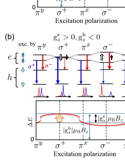
The upper panels of Fig. 2(a) and (b) are the excitation polarization dependence of the electron and hole energy states under affected by the generated in the cases of (a) , and (b) , . The dipole-allowed transitions with the PL polarization and the expected Zeeman-split spectra (red: , blue: ) are depicted schematically.
Since the angular momentum of a photon is transferred onto nuclei via the flip-flop term of HFI OptOrientation , a macroscopic nuclear spin polarization (NSP, ) which is orders of magnitude larger than the value in thermal equilibrium can be generated actually at cryogenic temperatures, and in turn, the resultant affects the electron spin states in the Zeeman splitting as well as the dynamics significantly Gammon01 ; Yokoi05 ; Kaji07 ; Chekhovich10 ; Urbaszek13 . Note that the affects only the electron states, not hole states because of the nonzero existence probability of the Bloch function at the nucleus site as shown in the energy diagrams of Fig. 2. For the linearly polarized excitation ( and ), the and polarized PL spectra should indicate in principle the equivalent PL intensity and the is determined only by (i.e., =0 if averaged electron spin polarization =0). In the case of 0, the nonzero is generated and affects the energy shift of the electron spin states.
The flip-flop term of the collinear HFI builds up the NSP always parallel to the electron spin ; becomes negative (positive) due to the negative (positive) injected optically by excitation. The -component of , , is written by = OptOrientation and the direction (sign) is determined by the signs of , and considering for III-V QDs. Although the sign of depends on the excitation polarization, is generated always antiparallel to for as shown in Fig. 2(a). Inversely, is generated parallel to for as shown in Fig. 2(b). Therefore, the compensation of positive with and NSSW occurs at excitation for . Note that the compensation by affects only the electron spin states.
The above mentioned excitation polarization dependence of the electron states is reflected directly to the change of affected by as shown in the lower panels of Fig. 2. When is formed antiparallel to , , thus , indicates the abrupt change by NSSW due to the positive feedback of the formation rate Maletinsky07 ; Urbaszek13 , and a large change of emerges. However, the change of by NSSW is observed as an abrupt reduction of for (Fig. 2(a)) and an abrupt increase of for (Fig. 2(b)).
The induced abrupt change of and the sign of are summarized in Table 1. In the cases of , the pattern of is shifted in negative region according to the definition of . Note that the change of by NSSW is determined by the product Kaji07 because the product determines that the pattern of the transitions with and polarizations as shown in the upper panels of Fig. 2(a) and (b); one is the included pattern (a) and the other is the nested pattern (b). In the figures of (lower panels), the Zeeman splitting of the hole spin states, , is indicated by a horizontal thin solid line. The variation from the thin line corresponds to the electron Zeeman splitting . Thus, the Zeeman splitting of two PL lines by the linearly polarized excitation (i.e. without ) is given by for the former pattern and for the latter pattern. Considering the sign of the g factors, the g factors of and can be written by . From Figs. 1 and 2, and (Fig. 2(b)) can be assigned for the observed single InAlAs QD. Although the magnitude and as well as the signs can be obtained from Fig. 1, the error of the magnitude has to be deduced from a more precise measurement by changing to a few values (not shown here). As a result, = 0.02 and =0.01 are obtained for the studied single InAlAs QD. In addition, the magnitude of the in-plane g factor (=0.350.01) and the in-plane anisotropy of the QD have been already reported Yamamoto18 . From the isotropic nature of the conduction band, the is considered to have a positive sign too.
| Sign of | change of | sign of | Fig. 2 | |
|---|---|---|---|---|
| by NSSW | ||||
| , | reduction | negative | ||
| , | reduction | positive | (a) | |
| , | increase | negative | ||
| , | increase | positive | (b) |
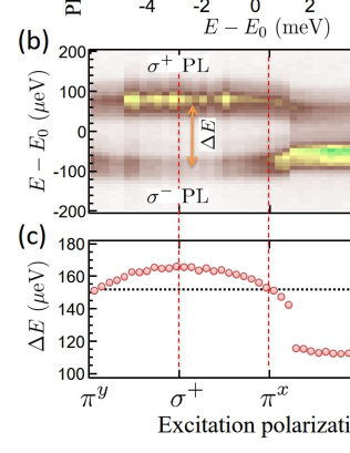
Next, the method is applied to identify the sign of g factors in single InAs/GaAs QRs. The averaged QR sizes are 40 nm in outer diameter, 10 nm in inner diameter, and 10 nm in height. The details of the growth conditions are seen in Ref. Tu_APL07, . The magnitude of out-of-plane (, ) and in-plane g factors (, ), and their anisotropy for many QRs are already reported in Refs. Kaji14, and Kaji_pssb17, . Under 1.0 T, the excitation polarization dependence measurements with the same setup as those in InAlAs QDs were carried out. The polarization-resolved PL spectra in Fig. 3(a) indicates very small FSS less than our spectral resolution, which is expected from the annealing in the process of QR formation from QD Tu_APL07 . Figure 3(b) shows a two-dimensional plot of the excitation polarization dependence of the PL spectra. The corresponding energy splitting () is plotted in Fig. 3(c). Unlike the case of InAlAs QDs, an abrupt reduction in was observed around the excitation, which corresponds to the response shown in Fig. 2(a), that is, and . Further, we confirmed that many other InAs QRs grown in the same sample indicated the similar responses (not shown here). Consequently, =0.02, =0.02 are obtained for this single InAs QR.
Previously, the sign of g factors of InGaAs/GaAs QDs was examined experimentally from the Zeeman splitting of bright and dark excitons, which is one of clear methods to determine the sign of g factors although it is necessary to select the QD with a reduced shape symmetry or tilted quantization axis. For In0.6Ga0.4As/GaAs QDs, = and = were reported Bayer99 , and the results were supported by the theoretical studies Nakaoka04 . The sign of g factors in InAs QRs coincides with the results in In(Ga)As QDs. From both measurements of Figs. 1 and 3, it is found that the sign of in InAlAs QDs is opposite to the one in InAs QRs while the signs of in the both systems are the same.
Finally, we confirm the conditions adopted in this work. From Figs. 1 and 3, it is clear that the DCP of the PL emission varies following the change of the excitation polarization, that is the case of a positive DCP. Here, the DCP is defined by with the integrated intensity of the polarized PL spectrum. It means that the optically-excited electron spin polarization was highly preserved right before the radiative recombination and contributes to form . If the negative DCP is observed for PL (i.e. the is flipped before the recombination from the ground state), the signs of and are reversed respectively. In the case of , the interacting electron spin that form by HFI is the remained electron spin after the radiative recombination. Therefore, the reversed electron spin is effective for formation in the positive DCP case. In contrast, when the hole spin in is flipped during the relaxation process to the ground state and the negative DCP is observed, the same spin as the optically-excited electron is effective for formation. We summarize the application of the proposed method to two charge states in Table 2.
| charge state of the ground level | ||
| DCP | ||
| positive | A | R |
| negative | R | A |
Before summarizing this work, we should denote the limitation of this sign identification method. Our method can be applied to the PLs of any charge states originated from single nanostructures like QDs of commonly used III-V direct-gap semiconductors as long as NSSW occurs there. This is because the III-V elements of the well-established compound semiconductors have non-zero nuclear spins with large natural abundance. The minimal magnitude of the g factors is 0.02 for evaluation in our current system, which depends basically on the spectral resolution (5 eV).
In summary, we demonstrated a convenient sign identification method of electron and hole out-of-plane g factors utilizing the correlation of NSSW and the sign of Zeeman splitting. The usefulness of the method was demonstrated for individual In0.75Al0.25As/Al0.3Ga0.7A QDs and InAs/GaAs QRs, where the sign of the electron g factor was different. Although we vary the excitation polarization systematically for the demonstration, the magnitude and sign of the out-of-plane g factors can be deduced by observation of the PL spectra at only three excitation polarization (or , , and under a positive . Further, this method offers advantages to evaluate the fluctuation of directly by combining the electron Zeeman part of and DCP in the case of Matsusaki17 .
The authors would like to acknowledge H. Sasakura in Hokkaido University and S.-J. Cheng in National Chiao-Tung University for helpful discussions. This work is supported by JSPS KAKENHI (Grants No. JP26800162 and No. JP17K19046) and the Asahi Glass Foundation (Japan).
References
- (1) Optical Orientation, Modern Problems in Condensed Matter Sciences Vol. 8, edited by F. Meier and B. Zakharchenya (North-Holland, NewYork, 1984).
- (2) Spin Physics in Semiconductors, Springer Series in Solid-State Sciences Vol. 157, edited by M. I. Dyakonov (Springer, Berlin, 2008).
- (3) S. E. Economou and T. L. Reinecke, Optically induced spin rotations in quantum dots in Optical Generation and Control of Quantum Coherence in Semiconductor Nanostructures, edited by G. Slavcheva and P. Roussignol, Chap. 5 (Springer-Verlag, Berlin, 2010).
- (4) A. J. Bennett, M. A. Pooley, Y. Cao, N. Sköld, I. Farrer, D. A. Ritchie, and A. J. Shields, Nat. Comm. 4, 1522 (2013).
- (5) T. Nakaoka, S. Tarucha, and Y. Arakawa, Phys. Rev. B 76, 041301(R) (2007).
- (6) H. M. G. A. Tholen, J. S. Wildmann, A. Rastelli, R. Trotta, C. E. Pryor, E. Zallo, O. G. Schmidt, P. M. Koenraad, and A. Yu. Silov, Phys. Rev. B 94, 245301 (2016).
- (7) M. J. Snelling, G. P. Flinn, A. S. Plaut, R. T. Harley, A. C. Tropper, R. Eccleston, C. C. Phillips, Phys. Rev. B 44, 11345 (1991).
- (8) A. A. Sirenko, T. Ruf, M. Cardona, D. R. Yakovlev, W. Ossau, A. Waag, G. Landwehr, Phys. Rev. B 56, 2114 (1997).
- (9) T. Nakaoka, T. Saito, J. Tatebayashi, and Y. Arakawa, Phys. Rev. B 70, 235337 (2004).
- (10) X. Marie, T. Amand, J. Barrau, P. Renucci, P. Lejeune, V. K. Kalevich, Phys. Rev. B 61, 11 065 (2000).
- (11) A. Malinowski and R. T. Harley, Phys. Rev. B 62, 2051 (2000).
- (12) G. Salis, D. D. Awschalom, Y. Ohno, and H. Ohno, Phys. Rev. B 64, 195304 (2001).
- (13) A. Malinowski, D. J. Guerrier, N. J. Traynor, and R. T. Harley, Phys. Rev. B 60, 7728 (1999).
- (14) O. Krebs, P. Maletinsky, T. Amand, B. Urbaszek, A. Lemaître, P. Voisin, X. Marie, and A. Imamoglu, Phys. Rev. Lett. 104, 056603 (2010).
- (15) S. Yamamoto, R. Matsusaki, R. Kaji, and S. Adachi, Phys. Rev. B 97, 075309 (2018).
- (16) M. Bayer, A. Kuther, A. Forchel, A. Gorbunov, V. B. Timofeev, F. Schäfer, and J. P. Reithmaier, Phys. Rev. Lett. 82, 1748 (1999).
- (17) E. A. Chekhovich, M. N. Makhonin, J. Skiba-Szymanska, A. B. Krysa, V. D. Kulakovskii, M. S. Skolnick, and A. I. Tartakovskii, Phys. Rev. B 81, 245308 (2010).
- (18) G. Sallen, B. Urbaszek, M. M. Glazov, E. L. Ivchenko, T. Kuroda, T. Mano, S. Kunz, M. Abbarchi, K. Sakoda, D. Lagarde, A. Balocchi, X. Marie, and T. Amand, Phys. Rev. Lett. 107, 166604 (2011).
- (19) R. Kaji, S. Adachi, H. Sasakura, and S. Muto, Appl. Phys. Lett. 91, 261904 (2007).
- (20) A. I. Tartakovskii, T. Wright, A. Russell, V. I. Fal’ko, A. B. Van’kov, J. Skiba-Szymanska, I. Drouzas, R. S. Kolodka, M. S. Skolnick, P. W. Fry, A. Tahraoui, H.-Y. Liu, and M. Hopkinson, Phys. Rev. Lett. 98, 026806 (2007).
- (21) R. Kaji, T. Hozumi, Y. Hachiyama, T. Tomii, H. Sasakura, M. Jo, and S. Adachi, Appl. Phys. Express 7, 065002 (2014).
- (22) T. Yokoi, S. Adachi, H. Sasakura, S. Muto, H. Z. Song, T. Usuki, and S. Hirose, Phys. Rev. B 71, 041307(R) (2005).
- (23) J. Debus, T. S. Shamirzaev, D. Dunker, V. F. Sapega, E. L. Ivchenko, D. R. Yakovlev, A. I. Toropov, and M. Bayer, Phys. Rev. B 90, 125431 (2014).
- (24) H. Kumano, S. Kimura, M. Endo, H. Sasakura, S. Adachi, S. Muto, and I. Suemune, J. Nanoelectron. Optoelectron. 1, 39 (2006).
- (25) R. Kaji, Doctoral Thesis, Hokkaido University, 2011.
- (26) H. Sasakura, R. Kaji, S. Adachi, S. Muto, Appl. Phys. Lett. 92, 041915 (2008).
- (27) Two definitions of the sign of hole g factor with the same Zeeman Hamiltonian has been used in the previous works; is assigned for the situation that the up-spin hole state has a higher energy and for the another situation that the up-spin valence electron state has a higher energy.
- (28) C. Testelin, F. Bernardot, B. Eble, and M. Chamarro, Phys. Rev. B 79, 195440 (2009).
- (29) D. Gammon, Al. L. Efros, T. A. Kennedy, M. Rosen, D. S. Katzer, D. Park, S. W. Brown, V. L. Korenev, and I. A. Merkulov, Phys. Rev. Lett. 86, 5176 (2001). Phys. Rev. B 74, 245306 (2006).
- (30) P. Maletinsky, C. W. Lai, A. Badolato, and A. Imamoglu, Phys. Rev. B 75, 035409 (2007).
- (31) Recent optical investigation of nuclear spin physics in QDs are reviewed comprehensively: B. Urbaszek, X. Marie, T. Amand, O. Krebs, P. Voisin, P. Maletinsky, A. Högele, A. Imamoglu, Rev. Mod. Phys. 85, 79 (2013).
- (32) S. Suraprapapich, S. Panyakeow, and C. W. Tu, Appl. Phys. Lett. 90, 183112 (2007).
- (33) R. Kaji, T. Tominaga, Y.-N. Wu, S.-J. Cheng, and S. Adachi, Phys. Status Solidi B 254, 1600486 (2017).
- (34) R. Matsusaki, R. Kaji, S.Yamamoto, H. Sasakura, and S.Adachi, arXiv:1703.06046.