Magnetic Tunnel Junction Performance Under Mechanical Strain
Abstract
In this work we investigate the effect of the mechanical stress on the performance of magnetic tunnel junctions (MTJ) with perpendicular magnetic anisotropy. We developed a 4-point bending setup, that allows us to apply a constant stress over a large substrate area with access to electrical measurements and external magnetic field. This setup enables us to measure key device performance parameters, such as tunnel magnetoresistance (TMR), switching current () and thermal stability (), as a function of applied stress. We find that variations in these parameters are negligible: less than over the entire measured range between the zero stress condition and the maximum stress at the point of wafer breakage.
Recently, several companies have announced successful integration of embedded Magnetic Random Access Memory (MRAM) with existing CMOS logic Kang (2014); Shum et al. (2017); Song et al. (2016). Spin transfer torque (STT) MRAM is a non-volatile memory technology that offers high speeds, low energy consumption and high endurance Apalkov et al. (2016); Kawahara et al. (2012). The fundamental building block of STT-MRAM is a magnetic tunnel junction (MTJ), which consists of two ferromagnetic layers separated by a tunneling barrier. Readout of the MRAM bit is enabled by the tunnel magnetoresistance (TMR) of the MTJ Julliere (1975); Moodera et al. (1995), while write operations are based on STT switching Berger (1996); Slonczewski (1996).
An important design parameter for MRAM is the strain applied to the ferromagnetic layers of the MTJ. Strain can impact the magnetic and electronic properties of a magnet as well as the quantum transport across the tunneling barrier. The TMR of a MTJ with in-plane anisotropy changes significantly under application of stress Loong et al. (2016). In fact, Loong et al. have seen an enhancement of the TMR by Loong et al. (2015) under the application of inhomogeneous strain. Furthermore, strain and pressure sensors based on the magneto elastic coupling of CoFe have been demonstrated Löhndorf et al. (2002); Tavassolizadeh et al. (2015, 2016); Meyners et al. (2009).
Previous work on the strain dependence of MTJs has focused on devices with in-plane magnetic anisotropy. State of the art memory elements, however, utilize MTJs having thinner free layers with out of plane anisotropy due to better scalability and faster switching times Sun (2000); Worledge et al. (2011); Nowak et al. (2011); Sato et al. (2013).
In this work we characterize MTJs with out of plane magnetic anisotropy under systematic application of strain. In addition to the TMR, we also study the strain dependence of other important performance parameters, such as the critical write current and the thermal stability factor . To apply the strain in a systematic way, we have designed an integrated 4-point bending setup Baril et al. (1999) with a magnetic probe station. This 4-point bending setup allows us to apply constant strain over large substrate areas while magnetotransport measurements are carried out.
We present the surprising result that transport in our MTJ devices with perpendicular magnetic anisotropy is very robust to mechanical stress. Our findings show that while the TMR and the thermal stability factor are independent of external strain (within the accuracy of the measurement), we observe a small decrease of the coercive field and the switching current with increasing strain.
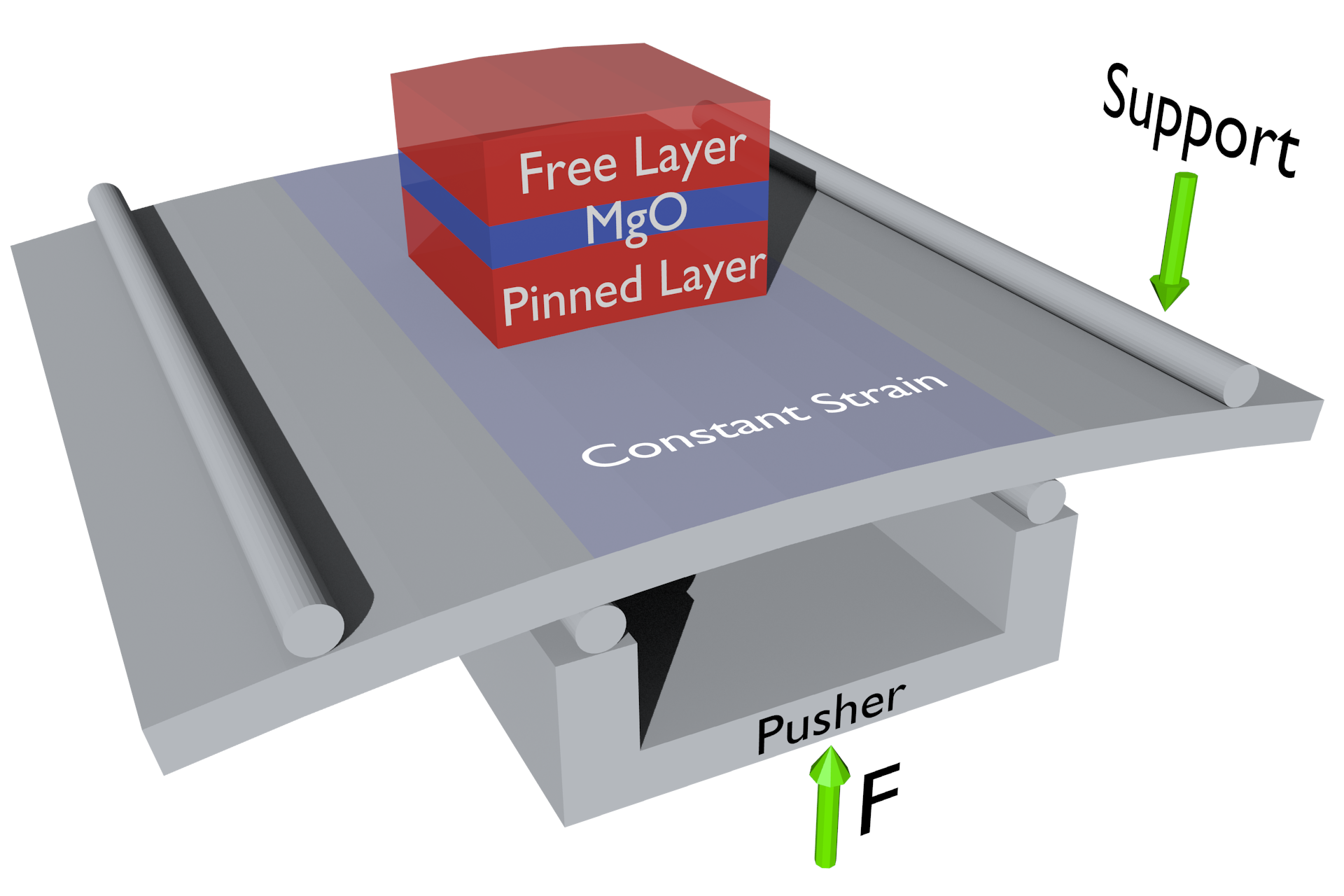
Figure 1 shows a sketch of our 4-point bending setup. Two ceramic rods support the wafer from the top while a force is applied from the bottom to bend the wafer. The strain in the center region between the two supporting rods is constant. This strain is related to the bending curvature as , where is the distance to the neutral plane, i.e the wafer thickness divided by 2.
The MTJs under investigation in this study are deposited on top of a thick silicon wafer with thermal oxide. The MTJ stack consists of a synthetic antiferromagnet, i.e. layered ferromagnets with antiferromagnetic coupling, serving as a reference (pinned) layer, and a CoFeB-based free layer separated by a MgO tunnel barrier. Both layers have perpendicular magnetic anisotropy. Tunnel junction devices are patterned, using conventional ion milling technique, into circles with diameter from . All measurements of the electrical resistance are performed in a two terminal geometry with the contact resistance taken into account.
To protect our samples from damage due to uncontrolled shattering we first examine the maximum strain that can be applied to the wafer before a catastrophic breakage event occurs. We find that the average breaking point of the silicon wafers used for this study is at . Assuming the value of for the Young’s modulus of silicon, this corresponds to a stress level of . To prevent wafer breakage, the maximum strain applied in this study is thus limited to .
We first measure -minor loops by sweeping an external magnetic field along the easy axis of the free layer. Figure 2(a) shows two switching events and clearly distinguishable high and low resistance states. The coercive field of the free layer as well as the TMR ratio are extracted from this measurement. A summary of the normalized TMR ratio and as a function of strain is shown on Fig. 2(b). Each value reflects the mean of 46 -loops on 63 different devices. The obtained values for the TMR ratio are remarkably constant over the whole range of strain, with variations less than . The coercive field decreases slightly with increasing strain. This decrease is attributed to the magnetoelastic coupling of the free layer.
Next, the critical current for spin-transfer torque switching is considered. We define the critical current as the current with 50% switching probability. Figure 3(a) shows as a function of the current pulse width . At long current pulses (), the switching process is thermally activated (cyan region) and depends logarithmically on Baril et al. (1999):
Here is the thermal stability, is the intrinsic attempt time and is the intrinsic switching current. The solid lines in Fig. 3(a) are fits to the model above. For short pulses with , precessional switching is observed, where Worledge et al. (2011). The dotted line in the yellow regime in Fig. 3(a) indicates this inverse trend.
The critical current at , , is shown as a function of strain in Fig. 3(b). As in Fig 2(b) we show the average value for 63 tested devices. For both switching directions, decreases with increasing strain. At strain, is reduced by . The decrease in is similar to the reduction in with increasing strain.
The thermal stability is derived from write error rate (WER) measurements. The switching probability is plotted as a function of current pulse amplitude in Fig. 4(a). We chose a pulse length of and measured deep error rates down to . The thermal stability is calculated according to Butler et al. (2012):
where is the extrapolated switching probability at .
Figure 4(b) shows , averaged for 63 devices, as a function of strain. is constant for all strain values tested. It should be noted that the noise in this measurement is on the order of of the mean value. Thus, if the change in is of the same order of magnitude as the change in or , it will not be detectable by this method.
In conclusion, we have measured MTJ performance parameters under the application of mechanical strain. The strain was applied in a 4-point bending geometry, where the strain is constant over a large substrate area. It is found that the TMR ratio as well as the thermal stability in the devices under test do not change as a function of strain within the measurement accuracy. The coercive field and the switching current decrease by approximately over the whole range of applied strain. A thinner free layer in our devices with PMA might contribute to the quantitative difference in the strain dependence of the TMR seen in previous work Loong et al. (2015, 2016). The result reported here has significant implications for the manufacturability of STT-MRAM, as strain is often the result of device encapsulation or CMOS passivation processes that are determined by BEOL requirements.
We thank Robert Beach and Volodymyr Voznyuk for fruitful discussions.
References
- Kang (2014) S. H. Kang, in 2014 Symposium on VLSI Technology (IEEE, 2014) pp. 1–2.
- Shum et al. (2017) D. Shum, D. Houssameddine, S. T. Woo, Y. S. You, J. Wong, K. W. Wong, C. C. Wang, K. H. Lee, K. Yamane, V. B. Naik, C. S. Seet, T. Tahmasebi, C. Hai, H. W. Yang, N. Thiyagarajah, R. Chao, J. W. Ting, N. L. Chung, T. Ling, T. H. Chan, S. Y. Siah, R. Nair, S. Deshpande, R. Whig, K. Nagel, S. Aggarwal, M. DeHerrera, J. Janesky, M. Lin, H.-J. Chia, M. Hossain, H. Lu, S. Ikegawa, F. B. Mancoff, G. Shimon, J. M. Slaughter, J. J. Sun, M. Tran, S. M. Alam, and T. Andre, in 2017 Symposium on VLSI Technology (IEEE, 2017) pp. T208–T209.
- Song et al. (2016) Y. J. Song, J. H. Lee, H. C. Shin, K. H. Lee, K. Suh, J. R. Kang, S. S. Pyo, H. T. Jung, S. H. Hwang, G. H. Koh, S. C. Oh, S. O. Park, J. K. Kim, J. C. Park, J. Kim, K. H. Hwang, G. T. Jeong, K. P. Lee, and E. S. Jung, in 2016 IEEE International Electron Devices Meeting (IEEE, 2016) pp. 27.2.1–27.2.4.
- Apalkov et al. (2016) D. Apalkov, B. Dieny, and J. M. Slaughter, Proceedings of the IEEE 104, 1796 (2016).
- Kawahara et al. (2012) T. Kawahara, K. Ito, R. Takemura, and H. Ohno, Microelectronics Reliability 52, 613 (2012).
- Julliere (1975) M. Julliere, Physics Letters A 54, 225 (1975).
- Moodera et al. (1995) J. S. Moodera, L. R. Kinder, T. M. Wong, and R. Meservey, Physical Review Letters 74, 3273 (1995).
- Berger (1996) L. Berger, Phys. Rev. B 54, 9353 (1996).
- Slonczewski (1996) J. C. Slonczewski, Journal of Magnetism and Magnetic Materials 159, L1 (1996).
- Loong et al. (2016) L. M. Loong, W. Lee, X. Qiu, P. Yang, H. Kawai, M. Saeys, J.-H. Ahn, and H. Yang, Advanced Materials 28, 4983 (2016).
- Loong et al. (2015) L. M. Loong, X. Qiu, Z. P. Neo, P. Deorani, Y. Wu, C. S. Bhatia, M. Saeys, and H. Yang, Scientific Reports 4, 6505 (2015).
- Löhndorf et al. (2002) M. Löhndorf, T. Duenas, M. Tewes, E. Quandt, M. Rührig, and J. Wecker, Applied Physics Letters 81, 313 (2002).
- Tavassolizadeh et al. (2015) A. Tavassolizadeh, P. Hayes, K. Rott, G. Reiss, E. Quandt, and D. Meyners, Journal of Magnetism and Magnetic Materials 384, 308 (2015).
- Tavassolizadeh et al. (2016) A. Tavassolizadeh, K. Rott, T. Meier, E. Quandt, H. Hölscher, G. Reiss, and D. Meyners, Sensors 16, 1902 (2016).
- Meyners et al. (2009) D. Meyners, T. von Hofe, M. Vieth, M. Rührig, S. Schmitt, and E. Quandt, Journal of Applied Physics 105, 07C914 (2009).
- Sun (2000) J. Z. Sun, Physical Review B 62, 570 (2000).
- Worledge et al. (2011) D. C. Worledge, G. Hu, D. W. Abraham, J. Z. Sun, P. L. Trouilloud, J. Nowak, S. Brown, M. C. Gaidis, E. J. O’Sullivan, and R. P. Robertazzi, Applied Physics Letters 98, 022501 (2011).
- Nowak et al. (2011) J. J. Nowak, R. P. Robertazzi, J. Z. Sun, G. Hu, D. W. Abraham, P. L. Trouilloud, S. Brown, M. C. Gaidis, E. J. O’Sullivan, W. J. Gallagher, and D. C. Worledge, IEEE Magnetics Letters 2, 3000204 (2011).
- Sato et al. (2013) H. Sato, M. Yamanouchi, S. Ikeda, S. Fukami, F. Matsukura, and H. Ohno, IEEE Transactions on Magnetics 49, 4437 (2013).
- Baril et al. (1999) L. Baril, B. Gurney, D. Wilhoit, and V. Speriosu, Journal of Applied Physics 85, 5139 (1999).
- Butler et al. (2012) W. H. Butler, T. Mewes, C. K. A. Mewes, P. B. Visscher, W. H. Rippard, S. E. Russek, and R. Heindl, IEEE Transactions on Magnetics 48, 4684 (2012).