Enhanced single photon emission from carbon nanotube dopant states coupled to silicon microcavities
Abstract
Single-walled carbon nanotubes are a promising material as quantum light sources at room temperature and as nanoscale light sources for integrated photonic circuits on silicon. Here we show that integration of dopant states in carbon nanotubes and silicon microcavities can provide bright and high-purity single photon emitters on silicon photonics platform at room temperature. We perform photoluminescence spectroscopy and observe enhancement of emission from the dopant states by a factor of 100, and cavity-enhanced radiative decay is confirmed using time-resolved measurements, where 30% decrease of emission lifetime is observed. Statistics of photons emitted from the cavity-coupled dopant states are investigated by photon correlation measurements, and high-purity single photon generation is observed. Excitation power dependence of photon emission statistics shows that the degree of photon antibunching can be kept low even when the excitation power increases, while single photon emission rate can be increased up to Hz.
Single photon emitters are a fundamental element for quantum information technologies O’Brien et al. (2009), and a wide range of materials has been explored to obtain ideal single photon emitting devices Aharonovich et al. (2016). In particular, semiconducting carbon nanotubes (CNTs) are regarded as a promising material for such an application because they are a nanoscale light emitting material Avouris et al. (2008) having stable excitonic states which arise from the one-dimensional structure of CNTs Wang et al. (2005); Maultzsch et al. (2005). Under cryogenic temperatures, excitons in CNTs are localized and behave as quantum-dot-like states Hofmann et al. (2016), exhibiting a quantum light signature Högele et al. (2008); Hofmann et al. (2013). At room temperature, single photon generation using CNTs has already been accomplished by two approaches Endo et al. (2015); Ma et al. (2015a); He et al. (2017); Ma et al. (2015b); Ishii et al. (2017). The first is where exciton trapping sites are created to localize excitons Ma et al. (2015a); He et al. (2017), and the second is where efficient exciton-exciton annihilation process is used to reduce the number of mobile excitons to unity Ma et al. (2015b); Ishii et al. (2017). The approach using exciton trapping sites allows for high purity single photon generation, use of chirality sorted CNTs, and direct deposition on various types of substrates. Furthermore, trapping sites protect excitons from quenching sites in CNTs, and optically-allowed defect states appear below the dark states of excitons, resulting in significant brightening of photoluminescence Piao et al. (2013); Miyauchi et al. (2013). Recently, aryl defects have received considerable attention because of the wide range of selectability of CNT chiralities, dopant species, and reaction conditions, which allows for tunable emission wavelength and decay lifetime Hartmann et al. (2016). Using this method, single photon generation with a purity of 99% and an emission wavelength of 1550 nm is achieved at room temperature He et al. (2017).
For practical single photon sources, not only single photon purity and operating temperature, but also emission wavelength, linewidth, brightness, and photon extraction efficiency are important. From this aspect, cavity structures are widely used to improve performances of single photon emitters Strauf et al. (2007); Englund et al. (2010); Kaupp et al. (2016). As for CNT single photon emitters, photonic Walden-Newman et al. (2012); Jeantet et al. (2016) and plasmonic Luo et al. (2017) cavity configurations have been used to enhance the brightness of single photon emission at low temperature. Further development is expected by integrating single photon emitters into silicon photonics because it can lead to on-chip integrated quantum devices Harris Nicholas et al. (2016), and CNTs have a potential for such an application due to their emission wavelengths having low transmission losses in silicon. Microcavities on silicon substrates have been used to enhance photoluminescence (PL) Watahiki et al. (2012); Noury et al. (2015) and Raman Sumikura et al. (2013) signal, and efficient coupling even to a single carbon nanotube has also been achieved Imamura et al. (2013); Miura et al. (2014); Machiya et al. (2018), demonstrating that CNTs are suitable for integration with silicon photonics.
Here we report on integration of CNT dopant state emitters with silicon microcavities. Emission from aryl defect states in CNTs coupled to two-dimensional photonic crystal microcavities is characterized by PL microscopy, and significant enhancement of PL intensity is observed. Time-resolved PL measurements on the same device show a direct evidence of enhanced emission decay rates by the Purcell effect, and we confirm single photon emission from the device by performing photon correlation measurements. The zero-delay second-order autocorrelation is as low as 0.1, showing high-purity single photon generation, and the value is stable even at high power excitation, which allows for single photon emission rates as high as Hz.
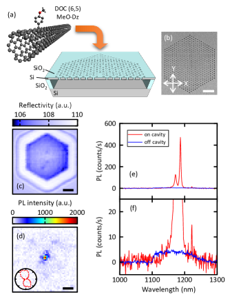
We start sample preparation by fabrication of photonic crystal microcavities on a silicon-on-insulator substrate [Fig. 1(a)]. Electron beam lithography defines the photonic crystal pattern with shift-L3 cavities Akahane et al. (2003), and the 200-nm-thick top Si layer is etched through by dry etching. The buried SiO2 layer with a thickness of 1000 nm is then etched by 20 wt% hydrofluoric acid, and thermal oxidation is performed at 900∘C for an hour to form a 10-nm-thick SiO2 layer on the top Si layer. A scanning electron micrograph of a typical device is shown in Fig. 1(b). Doped carbon nanotubes are prepared from chirality-enriched (6,5) CNTs encapsulated in a sodium deoxycholate (DOC) surfactant. Aryl functionalization is done using a diazonium dopant (4-methoxybenzenediazonium (MeO-Dz)), where the details are described in the literature Hartmann et al. (2015). We dilute the doped CNT solution with water to avoid bundling or piling up of CNTs on a substrate, and finally the solution is drop casted on the devices using a glass micropipette.
PL measurements are performed with a homebuilt sample-scanning confocal microscopy system Ishii et al. (2017). We use a Ti:sapphire laser where the output can be switched between continuous-wave (CW) and 100-fs pulses with a repetition rate of 76 MHz. We use an excitation wavelength of 855 nm, which matches the phonon side-band absorption for (6,5) CNTs Vora et al. (2010). The excitation laser beam with a power is focused onto the sample by an objective lens with a numerical aperture of 0.85. PL and the reflected beam are collected by the same objective lens and separated by a dichroic filter. A Si photodiode detects the reflected beam for imaging, while a translating mirror is used to switch between PL spectroscopy and time-resolved PL measurements. PL spectra are measured with an InGaAs photodiode array attached to a spectrometer. For time-resolved measurements, emission at around 1000 nm is filtered out by a wavelength-tunable band-pass filter with a transmission window of 10 nm or a long-pass filter with a cut-on wavelength of 1100 nm. Fiber-coupled two-channel superconducting single photon detector (SSPD) connected to a 50:50 signal-splitting fiber is used to perform PL decay and photon correlation measurements. All measurements are conducted at room temperature in a nitrogen-purged environment.
We perform automated collection of PL spectra Ishii et al. (2015) at all cavity positions to find devices with good optical coupling. For a device where a significant enhancement of the dopant state () emission Hartmann et al. (2016) is observed, reflectivity and PL images are taken [Figs. 1(c) and (d)]. The enhanced PL is localized at the center of the cavity, as expected from PL enhancement due to coupling with the resonance modes of the cavity. In Figs. 1(e) and (f), PL spectra on and off the cavity are shown, where the off-cavity signal is taken on the photonic crystal pattern. PL spectrum on the cavity shows multiple modes coupled to the dopant state emitters, while a broad emission peak from the dopant state is observed at the off-cavity position. In the on-cavity spectrum, the peak showing the highest intensity at an emission wavelength of 1187 nm has a full-width at half-maximum of 3.9 nm, corresponding to a quality factor . We assign the highest intensity peak to the 2nd mode of the L3 cavity Liu et al. (2015). By comparing the peak height of the on-cavity and off-cavity PL spectra, we obtain a PL enhancement factor of 100.
The PL enhancement can become large as there are other cavity-induced effects in addition to the Purcell effect. In our devices, it is known that localized guided modes can increase the excitation by more than a factor of 50 Liu et al. (2015), and coupling to such an absorption resonance can explain the strong excitation polarization dependence (inset of Fig. 1(d)). Furthermore, the directionality of the cavity radiation can improve the PL collection efficiency by as much as a factor of 4 Fujita et al. (2005). Combined with the Purcell effect, these cavity effects can significantly brighten the nanotube emitters, and thus the obtained enhancement factor of 100 would be a reasonable result.
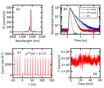
In order to investigate the Purcell enhancement of the radiative decay rate, we perform time-resolved PL measurements on the same device shown in Figs. 1(c-f). For on-cavity PL, a single peak is spectrally filtered by tuning the transmission wavelength of the band-pass filter [Fig. 2(a)], while the long-pass filter is used instead for off-cavity PL. In Fig. 2(b), PL decay curves taken at the on-cavity and off-cavity positions are shown, and fits are performed using a mono-exponential decay function convoluted with a Gaussian profile representing the instrument response function (IRF) of the system. Although PL decay of doped CNTs typically exhibits a bi-exponential curve Hartmann et al. (2016); He et al. (2017), here we use a mono-exponential decay for simplicity. From the fits, we obtain the on-cavity PL lifetime ps and the off-cavity PL lifetime ps. If we assume the radiative quantum efficiency of 2.4%, which is estimated by the unaffected quantum efficiency of 11% for MeO-Dz doped (6,5) CNTs in water Piao et al. (2013) and PL quenching by a factor of 4.5 caused by an interaction with the SiO2 substrate He et al. (2017), the 30% reduction of the emission lifetime corresponds to a Purcell factor , a coupling factor , and an enhanced radiative quantum efficiency of 31%.
We perform such lifetime measurements on ten other devices and obtain an average lifetime of 131.243.8 ps. The lifetime varies on different devices, suggesting that coupling is affected by some uncontrolled factors. Coupling efficiency is in general affected by spectral overlap, spatial overlap, and polarization overlap between the emitters and cavity modes. Moreover, CNT density fluctuations may have a significant effect in our samples. We note that variations in the cavity quality factors are not the main reason because of dopant state emission is much lower than that of the cavity peak.
Next we measure photon correlation for the same cavity peak shown in Figs. 2(a) and (b), and clear photon antibunching is observed as shown in Fig. 2(c). We evaluate the normalized second-order autocorrelation at zero time delay from the autocorrelation histogram by subtracting the dark counts and binning each peak with a binning width of 2 ns. We note that the histogram is taken within a time window from 60 to 300 ns, and side peaks after ns are used for normalization to avoid underestimation due to photon bunching. For the data shown in Fig. 2(c), we obtain , indicating high-purity single photon emission.
It is surprising that we obtain such high-purity single photon emission from a sample with drop-casted CNTs, where numerous emitters are expected within the laser spot. One explanation is that cavity coupling and spectral filtering allow selective photon collection from a few number of emitters. In fact, we actually observe higher when the band-pass filter is removed [Supporting Information S1]. It is worth mentioning that we could not measure photon correlation of off-cavity signal as the emission intensity is too low, indicating the advantages of cavity coupling.
During the photon correlation measurements, time traces of the photon detection rate are also recorded [Fig. 2(d)]. The total photon detection rate , defined as the sum of detection rates at the two channels, is obtained from the autocorrelation count rate using the relation
| (1) |
where is the signal splitting ratio between the two channels, and ns is the effective time window for the 27 peaks which are included in the correlation histograms [Supporting Information S2]. In Fig. 2(d), the PL intensity shows a relatively large fluctuation over time, whose standard deviation is 23 times larger than that of shot-noise limited fluctuation. We observe such intensity fluctuation of the cavity-coupled peak for all devices we have measured, which may be caused by the influence of the substrate Walden-Newman et al. (2012).
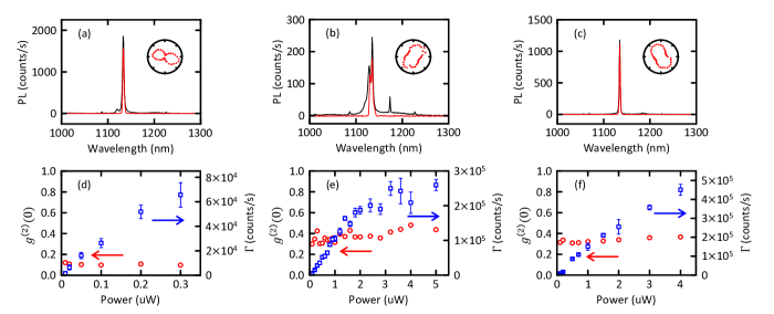
Finally, we investigate excitation power dependence of photon emission statistics on three other devices. The PL spectra on the cavities with and without the band-pass filter are shown in Figs. 3(a-c). For these spectrally filtered peaks, we measure and [Figs. 3(d-f)] while increasing until shows a rapid drop, which indicates deterioration of the devices. As increases, increases linearly while remains almost constant, except for the high power region in Fig. 3(e), where saturates and slightly increases. In all devices, remains lower than 0.5 throughout the range of , indicating the robustness of the quantum light signature. This behavior parallels the previous report He et al. (2017) where defect states for CNTs on a polymer film can also show excellent values even at relatively high pump powers. At W in Fig. 3(f), we obtain the highest of counts/s. We note that clear bunching is observed when is high [Supporting Information S3], which may be caused by an increase of background signals from CNTs which are not coupled to the cavity mode.
In the four devices for which we have measured the photon statistics, we find a positive correlation between single-photon purity and the degree of polarization , which is defined by
| (2) |
where and are the highest and lowest PL intensity, respectively, obtained by fitting the excitation polarization dependence to a sine function [insets of Fig. 1(d) and Figs 3(a-c)]. For the two devices whose are shown in Fig. 2(c) and Fig. 3(d), we obtain and , while and are obtained for the other two devices. This correlation is reasonable, because low implies that the CNT axis and the localized guided mode polarization do not match or that multiple CNTs with different orientations are coupling to the same mode of the cavity. This observation suggests that controlling the CNT density and orientation on the cavities is a key factor to obtain high quality single photon emitting devices.
The obtained values of can be converted to actual photon emission rates at the devices using the total photon collection efficiency in our optical system, which is estimated to be 2.6% [Supporting Information S4]. For the highest photon detection rate counts/s in our measurements, we obtain the corresponding photon emission rate of photons/s. By considering the laser pulse repetition rate of Hz, the photon emission rate corresponds to the single photon emission efficiency of 22%, which is consistent with the estimated quantum efficiency by the lifetime shortening observed in time-resolved measurements. Compared to the previously reported value for similar aryl-functionalized CNTs but wrapped by PFO-bpy and deposited onto a Au-deposited substrate with a separation layer of 160-nm-thick polystyrene He et al. (2017), the single photon emission efficiency is almost two times higher.
For achieving further improvement of our devices, optimization of CNT concentration is a key factor as mentioned above. Lowering the CNT density down to an individual CNT level will produce an ideal situation for cavity coupling, but such low density of CNTs results in extremely low yield of cavity-coupled devices. Once appropriate conditions for CNT deposition are determined, spin-coating can be used to obtain more uniform and reproducible deposition of CNTs on cavities Watahiki et al. (2012), which enables fabrication of integrated quantum light emitters on silicon chips. As another approach, position-controlled limited-area deposition using a micropipette or nano-droplet Galliker et al. (2012); Kress et al. (2014) may yield better results because it does not degrade the cavity quality, although such small-volume CNT deposition only at the cavity positions is challenging in practice. Improvement of cavity-coupling efficiency by avoiding quenching from substrates may be possible by using a thinner and more efficient separation layer, like hexagonal boron nitride thin films Kim et al. (2012). In addition, the relationship between coupling efficiency and cavity modes is worth investigating, where quality factor and mode profile are different depending on the mode order Chalcraft et al. (2007); Fujita et al. (2008). Larger mode volumes are beneficial for obtaining coupling to CNTs on the substrate but results in a lower Purcell effect at the same time. Finally we comment on the tunability of our devices. The emission wavelength of aryl functionalized CNTs can be tuned by selecting chiralities and dopant species Hartmann et al. (2016); He et al. (2017), and photonic crystal microcavities have a high flexibility both for absorption and emission resonances Liu et al. (2015). Our approach should therefore lead to bright single photon emitters at 1550 nm. In principle, it should also be possible to obtain indistinguishable single photon sources at room temperature by using higher quality cavities.
In summary, we demonstrate integration of carbon nanotube dopant state emitters with silicon microcavities, and PL characteristics and photon statistics of the devices are investigated. PL intensity enhancement by a factor of 100 is observed from the dopant state emission coupled to the cavity mode, and time-resolved measurements reveal a 30% lifetime shortening by the Purcell effect on the cavity-coupled emission. Photon correlation measurements are performed on the devices, and we confirm that room-temperature single photon emission capability, a key feature of -doped CNTs, is preserved in the cavity-enhanced PL emission. We obtain as low as 0.1 and find that the degree of photon antibunching is stable over a wide range of excitation power. By increasing the excitation power, we obtain a single photon detection rate as high as Hz, which corresponds to a single photon emission rate of Hz and a single photon emission efficiency of 22% per laser pulse. Our results indicate that integration of dopant state emitters in CNTs with silicon microcavities can provide bright and high-purity quantum light sources at room temperature on silicon photonics platform, raising expectations toward integrated quantum photonic devices.
Supporting Information
See supporting information for autocorrelation histograms taken with and without the band-pass filter, derivation of , excitation power dependence of autocorrelation histograms, and estimation of photon collection efficiency of the system.
Acknowledgements.
Work supported by JSPS (KAKENHI JP16K13613, JP17H07359) and MEXT (Photon Frontier Network Program, Nanotechnology Platform). A.I. acknowledges support from MERIT, and H.M. is supported by RIKEN Junior Research Associate Program. We thank Advanced Manufacturing Support Team at RIKEN for their assistance in machining. This work was conducted in part at the Center for Integrated Nanotechnologies, a US Department of Energy, Office of Science user facility and supported in part by Los Alamos National Laboratory Directed Research and Development funds.References
- O’Brien et al. (2009) J. L. O’Brien, A. Furusawa, and J. Vučkovic, Photonic quantum technologies, Nat. Photon. 3, 687 (2009).
- Aharonovich et al. (2016) I. Aharonovich, D. Englund, and M. Toth, Solid-state single-photon emitters, Nat. Photon. 10, 631 (2016).
- Avouris et al. (2008) P. Avouris, M. Freitag, and V. Perebeinos, Carbon-nanotube photonics and optoelectronics, Nat. Photon. 2, 341 (2008).
- Wang et al. (2005) F. Wang, G. Dukovic, L. E. Brus, and T. F. Heinz, The optical resonances in carbon nanotubes arise from excitons, Science 308, 838 (2005).
- Maultzsch et al. (2005) J. Maultzsch, R. Pomraenke, S. Reich, E. Chang, D. Prezzi, A. Ruini, E. Molinari, M. S. Strano, C. Thomsen, and C. Lienau, Exciton binding energies in carbon nanotubes from two-photon photoluminescence, Phys. Rev. B 72, 241402(R) (2005).
- Hofmann et al. (2016) M. S. Hofmann, J. Noé, A. Kneer, J. J. Crochet, and A. Högele, Ubiquity of exciton localization in cryogenic carbon nanotubes, Nano Lett. 16, 2958 (2016).
- Högele et al. (2008) A. Högele, C. Galland, M. Winger, and A. Imamoğlu, Photon antibunching in the photoluminescence spectra of a single carbon nanotube, Phys. Rev. Lett. 100, 217401 (2008).
- Hofmann et al. (2013) M. S. Hofmann, J. T. Glückert, J. Noé, C. Bourjau, R. Dehmel, and A. Högele, Bright, long-lived and coherent excitons in carbon nanotube quantum dots, Nat. Nanotech. 8, 502 (2013).
- Endo et al. (2015) T. Endo, J. Ishi-Hayase, and H. Maki, Photon antibunching in single-walled carbon nanotubes at telecommunication wavelengths and room temperature, Appl. Phys. Lett. 106, 113106 (2015).
- Ma et al. (2015a) X. Ma, N. F. Hartmann, J. K. S. Baldwin, S. K. Doorn, and H. Htoon, Room-temperature single-photon generation from solitary dopants of carbon nanotubes, Nat. Nanotech. 10, 671 (2015a).
- He et al. (2017) X. He, N. F. Hartmann, X. Ma, Y. Kim, R. Ihly, J. L. Blackburn, W. Gao, J. Kono, Y. Yomogida, A. Hirano, T. Tanaka, H. Kataura, H. Htoon, and S. K. Doorn, Tunable room-temperature single-photon emission at telecom wavelengths from defects in carbon nanotubes, Nat. Photon. 11, 577 (2017).
- Ma et al. (2015b) X. Ma, O. Roslyak, J. G. Duque, X. Pang, S. K. Doorn, A. Piryatinski, D. H. Dunlap, and H. Htoon, Influences of exciton diffusion and exciton-exciton annihilation on photon emission statistics of carbon nanotubes, Phys. Rev. Lett. 115, 017401 (2015b).
- Ishii et al. (2017) A. Ishii, T. Uda, and Y. Kato, Room-temperature single-photon emission from micrometer-long air-suspended carbon nanotubes, Phys. Rev. Applied 8, 054039 (2017).
- Piao et al. (2013) Y. Piao, B. Meany, L. R. Powell, N. Valley, H. Kwon, G. C. Schatz, and Y. Wang, Brightening of carbon nanotube photoluminescence through the incorporation of defects, Nat. Chem. 5, 840 (2013).
- Miyauchi et al. (2013) Y. Miyauchi, M. Iwamura, S. Mouri, T. Kawazoe, M. Ohtsu, and K. Matsuda, Brightening of excitons in carbon nanotubes on dimensionality modification, Nat. Photon. 7, 715 (2013).
- Hartmann et al. (2016) N. F. Hartmann, K. A. Velizhanin, E. H. Haroz, M. Kim, X. Ma, Y. Wang, H. Htoon, and S. K. Doorn, Photoluminescence dynamics of aryl sp3 defect states in single-walled carbon nanotubes, ACS Nano 10, 8355 (2016).
- Strauf et al. (2007) S. Strauf, N. G. Stoltz, M. T. Rakher, L. A. Coldren, P. M. Petroff, and D. Bouwmeester, High-frequency single-photon source with polarization control, Nat. Photon. 1, 704 (2007).
- Englund et al. (2010) D. Englund, B. Shields, K. Rivoire, F. Hatami, J. Vučković, H. Park, and M. D. Lukin, Deterministic coupling of a single nitrogen vacancy center to a photonic crystal cavity, Nano Lett. 10, 3922 (2010).
- Kaupp et al. (2016) H. Kaupp, T. Hümmer, M. Mader, B. Schlederer, J. Benedikter, P. Haeusser, H.-C. Chang, H. Fedder, T. W. Hänsch, and D. Hunger, Purcell-enhanced single-photon emission from nitrogen-vacancy centers coupled to a tunable microcavity, Phys. Rev. Applied 6, 054010 (2016).
- Walden-Newman et al. (2012) W. Walden-Newman, I. Sarpkaya, and S. Strauf, Quantum light signatures and nanosecond spectral diffusion from cavity-embedded carbon nanotubes, Nano Lett. 12, 1934 (2012).
- Jeantet et al. (2016) A. Jeantet, Y. Chassagneux, C. Raynaud, P. Roussignol, J. S. Lauret, B. Besga, J. Estève, J. Reichel, and C. Voisin, Widely tunable single-photon source from a carbon nanotube in the Purcell regime, Phys. Rev. Lett. 116, 247402 (2016).
- Luo et al. (2017) Y. Luo, E. D. Ahmadi, K. Shayan, Y. Ma, K. S. Mistry, C. Zhang, J. Hone, J. L. Blackburn, and S. Strauf, Purcell-enhanced quantum yield from carbon nanotube excitons coupled to plasmonic nanocavities, Nat. Commun. 8, 1413 (2017).
- Harris Nicholas et al. (2016) C. Harris Nicholas, B. Darius, P. Mihir, R. Steinbrecher Greg, M. Jacob, P. Mihika, B.-J. Tom, H. Michael, and E. Dirk, Large-scale quantum photonic circuits in silicon, Nanophotonics 5, 456 (2016).
- Watahiki et al. (2012) R. Watahiki, T. Shimada, P. Zhao, S. Chiashi, S. Iwamoto, Y. Arakawa, S. Maruyama, and Y. K. Kato, Enhancement of carbon nanotube photoluminescence by photonic crystal nanocavities, Appl. Phys. Lett. 101, 141124 (2012).
- Noury et al. (2015) A. Noury, X. L. Roux, L. Vivien, and N. Izard, Enhanced light emission from carbon nanotubes integrated in silicon micro-resonator, Nanotechnology 26, 345201 (2015).
- Sumikura et al. (2013) H. Sumikura, E. Kuramochi, H. Taniyama, and M. Notomi, Cavity-enhanced Raman scattering of single-walled carbon nanotubes, Appl. Phys. Lett. 102, 231110 (2013).
- Imamura et al. (2013) S. Imamura, R. Watahiki, R. Miura, T. Shimada, and Y. K. Kato, Optical control of individual carbon nanotube light emitters by spectral double resonance in silicon microdisk resonators, Appl. Phys. Lett. 102, 161102 (2013).
- Miura et al. (2014) R. Miura, S. Imamura, R. Ohta, A. Ishii, X. Liu, T. Shimada, S. Iwamoto, Y. Arakawa, and Y. K. Kato, Ultralow mode-volume photonic crystal nanobeam cavities for high-efficiency coupling to individual carbon nanotube emitters, Nat. Commun. 5, 5580 (2014).
- Machiya et al. (2018) H. Machiya, T. Uda, A. Ishii, and Y. K. Kato, Spectral tuning of optical coupling between air-mode nanobeam cavities and individual carbon nanotubes, Appl. Phys. Lett. 112, 021101 (2018).
- Akahane et al. (2003) Y. Akahane, T. Asano, B.-S. Song, and S. Noda, High- photonic nanocavity in a two-dimensional photonic crystal, Nature 425, 944 (2003).
- Hartmann et al. (2015) N. F. Hartmann, S. E. Yalcin, L. Adamska, E. H. Haroz, X. Ma, S. Tretiak, H. Htoon, and S. K. Doorn, Photoluminescence imaging of solitary dopant sites in covalently doped single-wall carbon nanotubes, Nanoscale 7, 20521 (2015).
- Vora et al. (2010) P. M. Vora, X. Tu, E. J. Mele, M. Zheng, and J. M. Kikkawa, Chirality dependence of the -momentum dark excitons in carbon nanotubes, Phys. Rev. B 81, 155123 (2010).
- Ishii et al. (2015) A. Ishii, M. Yoshida, and Y. K. Kato, Exciton diffusion, end quenching, and exciton-exciton annihilation in individual air-suspended carbon nanotubes, Phys. Rev. B 91, 125427 (2015).
- Liu et al. (2015) X. Liu, T. Shimada, R. Miura, S. Iwamoto, Y. Arakawa, and Y. K. Kato, Localized guided-mode and cavity-mode double resonance in photonic crystal nanocavities, Phys. Rev. Applied 3, 014006 (2015).
- Fujita et al. (2005) M. Fujita, S. Takahashi, Y. Tanaka, T. Asano, and S. Noda, Simultaneous inhibition and redistribution of spontaneous light emission in photonic crystals, Science 308, 1296 (2005).
- Galliker et al. (2012) P. Galliker, J. Schneider, H. Eghlidi, S. Kress, V. Sandoghdar, and D. Poulikakos, Direct printing of nanostructures by electrostatic autofocussing of ink nanodroplets, Nat. Commun. 3, 890 (2012).
- Kress et al. (2014) S. J. P. Kress, P. Richner, S. V. Jayanti, P. Galliker, D. K. Kim, D. Poulikakos, and D. J. Norris, Near-field light design with colloidal quantum dots for photonics and plasmonics, Nano Lett. 14, 5827 (2014).
- Kim et al. (2012) K. K. Kim, A. Hsu, X. Jia, S. M. Kim, Y. Shi, M. Dresselhaus, T. Palacios, and J. Kong, Synthesis and characterization of hexagonal boron nitride film as a dielectric layer for graphene devices, ACS Nano 6, 8583 (2012).
- Chalcraft et al. (2007) A. R. A. Chalcraft, S. Lam, D. O’Brien, T. F. Krauss, M. Sahin, D. Szymanski, D. Sanvitto, R. Oulton, M. S. Skolnick, A. M. Fox, D. M. Whittaker, H.-Y. Liu, and M. Hopkinson, Mode structure of the L3 photonic crystal cavity, Appl. Phys. Lett. 90, 241117 (2007).
- Fujita et al. (2008) M. Fujita, Y. Tanaka, and S. Noda, Light emission from silicon in photonic crystal nanocavity, IEEE J. Sel. Top. Quantum Electron. 14, 1090 (2008).