Topological Aspect of Graphene Patchwork with Regular Arrays of Nano Holes
Abstract
Triangular and honeycomb lattices are dual to each other – if we puncture holes into a featureless plane in a regular triangular alignment, the remaining body looks like a honeycomb lattice, and vice versa, if the holes are in a regular honeycomb alignment, the remaining body has a feature of triangular lattice. In this work, we reveal that the electronic states in graphene sheets with nano-sized holes in triangular and honeycomb alignments are also dual to each other in a topological sense. Namely, a regular hole array perforated in graphene can open a band gap in the energy-momentum dispersion of relativistic electrons in the pristine graphene, and the insulating states induced by triangular and honeycomb hole arrays are distinct in topology. In a graphene patchwork with regions of these two hole arrays put side by side counterpropagating topological currents emerge at the domain wall. This observation indicates that the cerebrated atomically thin sheet is where topological physics and nanotechnology meet.
Electrons behave as waves in microscopic world, and a regular array of scattering centers causes quantum interference, i.e., Bragg reflection, which governs the electron propagation in terms of energy and momentum. This explains band gaps and band insulators in crystals where ions are regularly aligned. The same principle is effective even if we zoom out a little bit: starting from Bloch waves, with which angstrom-scale structures of the underlying crystal are already taken into account, superstructures in micro- or meso-scopic scales can induce new band gaps and modify the electron propagation. The first example is the superlattice invented by Leo Esaki in order to control properties of semiconductors Esaki and Tsu (1970).
In this regard, graphene – mono atomic sheet of carbon atoms in honeycomb structure Novoselov et al. (2005) – is a promising playground. First, the honeycomb array of scattering centers is responsible for the most striking feature of graphene, emergent relativistic fermion Geim and Novoselov (2007); Castro Neto et al. (2009) appearing as an isolated gap closing point associated with linear dispersion (Dirac cone) in the band structure. Secondly, graphene is amiable to nano structuring Park et al. (2008a, b); Guinea et al. (2010). One idea is to introduce a regular array of holes, also known as antidot lattice, into graphene, with the remaining body dubbed as graphene nanomesh Shima and Aoki (1993); Pedersen et al. (2008); Sinitskii and Tour (2010); Bai et al. (2010); Zhu et al. (2014); Liu et al. (2014); Kazemi et al. (2015); Sandner et al. (2015); Gao et al. (2017). Depending on the hole alignment, the band structure of superstructured graphene can be either gapless or gapped, and in gapped cases the gap size is tunable Shima and Aoki (1993); Pedersen et al. (2008); Fürst et al. (2009); Guinea and Low (2010); Petersen et al. (2011); Baskin and Král (2011); Cui et al. (2011); Oswald and Wu (2012); Liu et al. (2013); Dvorak et al. (2013); Ouyang et al. (2014).
Historically, gap introduction in a honeycomb lattice model, or mass attachment to emergent relativistic electrons, has been cornerstones in discovering new topological phases of matter. For instance, with an appropriate time reversal symmetry (TRS) breaking term, the honeycomb lattice model can derive the quantum anomalous Hall state Haldane (1988), which is a typical topological state characterized by the Chern number Weng et al. (2015). When the spin-orbit coupling (SOC) is considered in a honeycomb lattice model, one obtains the quantum spin Hall (QSH) insulator Kane and Mele (2005a, b), which is also known as a topological insulator specified by a index. Recently, it is recognized that detuning the nearest-neighbor hopping integrals in the tight-binding model in honeycomb lattice also achieves a topological state characterized by mirror winding numbers Wu and Hu (2016); Kariyado and Hu (2017), i.e., a topological state protected by crystalline symmetry Fu (2011); Chiu et al. (2016). Yet, it is a challenging issue to have sizable topological gap in this scheme, since it involves angstrom scale manipulation in the hopping integrals.
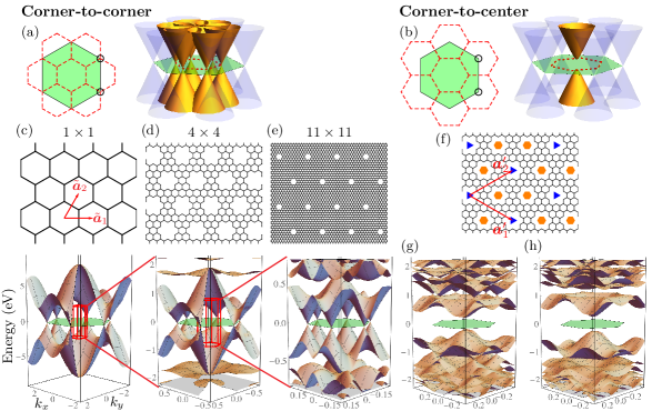
Here we propose a new strategy to realize topological states in graphene. Our recipe is divided into two steps, scaling and gap-opening. In the scaling step, a superstructure preserving the Dirac cones at the Brillouin zone (BZ) corner is introduced by puncturing triangular array of nano-sized holes into graphene [See Fig. 1(a)]. This process generates an electronic band structure similar to that of pristine graphene but with different length and energy scales, which permits one to work on an experimentally feasible length scale. In the next gap-opening step, we modify the triangular hole array by filling a subset of holes such that the Dirac cones at the BZ corners are brought to the zone center [See Fig. 1(b)] and gapped out. There are two kinds of superstructure in the second step, namely a triangular hole array and a honeycomb hole array. We reveal that graphene sheets with these two hole arrays are distinct in topology, and putting them side by side, which we call graphene patchwork, induces counterpropagating topological states at the domain wall. Noticing that to create nontrivial topology in electronic systems in terms of implanting nanostructures is attracting considerable current interests Sushkov and Castro Neto (2013); Wang et al. (2017); Jin et al. (2017); Cao et al. (2017), our new finding adds a new facet in this promising derection that intertwines topological physics and nanotechnology.
Model
For simplicity, we describe the electronic property of both the pristine
graphene and that with nano-sized holes in terms of a tight-binding
model on the honeycomb lattice where only the nearest neighbor hopping
eV is taken into account Castro Neto and Guinea (2007). Later, this
simplification is justified by band calculations based on density
functional theory (DFT). We start with the hexagonal hole where six
carbon atoms are removed from graphene as shown in
Figs. 1(d) and 1(e), and other
nano-sized holes will be discussed in the latter part of this paper. We
define in Fig. 1(c) as the unit
vectors for the pristine graphene, and the holes are arranged into a
triangular lattice with unit vectors
.
Realizing Topologically Distinct States
It is noticed that the integer defining lattice
constant of hole array influences the
low-energy electronic structure significantly
Liu et al. (2009); Ouyang et al. (2011); Lee et al. (2013). The
system is gapless for with integer , where the band
structures of the pristine graphene and the superstructured one are
related to each other by a corner-to-corner folding of the
Brillouin zone
Guinea and Low (2010); Dvorak et al. (2013) [See Fig. 1(a).] These
superstructures serve a good candidate for the first scaling
step, where the low-energy band structure is similar to the band
structure of pristine graphene with certain energy-scale
renormalization, and specifically Dirac cones at the Brillouin zone (BZ)
corners are preserved, as confirmed in Figs. 1(c), (d)
and (e), for pristine graphene, and graphene with hole arrays of
and respectively. The energy scale is
roughly proportional to the inverse of the superstructure length-scale,
reflecting the linear relation between energy and momentum of the Dirac
cone.
In order to implement the second gap-opening step, we selectively fill (i) the holes marked with (blue) triangles in Fig. 1(f) leaving a honeycomb array of holes, or (ii) the ones with (orange) hexagons leaving a triangular array of holes. With new unit vectors and , this operation corresponds to a length scaling of in addition to the one, which induces a corner-to-center BZ folding as shown in Fig. 1(b). This operation generates an energy gap of 0.45 eV and 0.52 eV for the honeycomb and triangular hole arrays, respectively [See Figs. 1(g) and 1(h)].
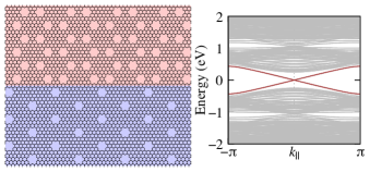
Now we show that the two insulating states induced by the honeycomb and triangular hole arrays are distinct in topology by means of the interface states. We prepare a “patchworked” graphene sheet having two regions with the honeycomb and triangular hole arrays side by side as schematically illustrated in Fig. 2, and calculate the band structure as a function of the momentum parallel to the interface . Figure 2 clearly shows cross-shape interface states (brown lines) in the energy range of the bulk gap. This emergent dispersive and counterpropagating interface states resemble the helical edge state in QSH effect.
Characterization of the Bulk Bands
The topological nature of the states under consideration
becomes clearer if we inspect the Bloch wave functions of the
bulk states in terms of the crystalline symmetries, especially
the point group symmetries Po et al. (2017); Bradlyn et al. (2017); Kruthoff et al. . Since
the two superstructures (honeycomb and triangle) share the same
symmetry, their band topology can be specified by the numbers of states
with even parity () and odd parity () against rotation
(equivalent to two-dimensional spatial inversion) Noh et al. .
As summarized in Table 1, for the honeycomb hole array
one finds in the valence bands at both
and M points, specifying a topologically trivial state. In contrary,
for the triangular array they are given by at
point different from that at M point ,
indicating a topological state. As will be discussed later, this result
can be understood in a simple way that the order of the parity even and
odd states at point is exchanged between the honeycomb and
triangular hole arrays, which reverse the sign of mass attached to the
relativistic fermion in the pristine graphene.
| structure | honeycomb | triangular |
|---|---|---|
| 21,21;21,21 | 24,21;22,23 | |
| 36,33;34,35 | 36,36;36,36 |
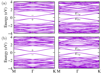
So far, the simple tight-binding model has been employed in our analysis. In order to confirm its validity, we also perform DFT calculations, where the perimeters of holes are terminated by hydrogen atoms Tang et al. (2017), and band structures are evaluated after structural optimization. For a direct comparison, the band structures obtained by the tight-binding model and DFT calculations are displayed on the left and right column of Fig. 3, respectively. Overall they agree well with each other, with the band gaps obtained by DFT calculations for both the honeycomb hole array (upper panels) and the triangular hole array (lower panels) being slightly larger than that evaluated by the tight-binding model. Deviations in detailed band structures are found away from the band gap at zero energy, which are unimportant for topological properties. The agreement between the two approaches is satisfactory considering that lattice deformations around holes correctly captured in DFT calculations are neglected in the simple tight-binding model where the hopping integral is presumed uniform in the whole system. Within DFT calculation, we also inspect the parity of wave functions. As is shown explicitly in the right column of Fig. 3, the order of the and states are exchanged between the honeycomb [Fig. 3(a)] and triangular [Fig. 3(b)] hole arrays, in agreement with the results derived with the tight-binding model as shown in the left column. Note that the symmetry operations in DFT calculations are 3D, and the states near the Fermi energy stem from -orbitals. Consequently, the even/odd parity state corresponds to an odd/even parity state against the rotation. From these comparisons, we conclude that the simple tight-binding model successfully captures the essence of gap opening in the superstructured graphene systems, and the topological interface states obtained within this model as shown in Fig. 2 are reliable.
Discussions
In order to see the interface states, we have used the interface along the direction of zigzag edge, for which the mirror winding
number can be assigned with the mirror plane perpendicular to the
interface Kariyado and Hu (2017). For interfaces
along the direction of armchair edge, a mini energy gap may open in
the interface modes, since the mirror operation mixes the two
sublattices of graphene Kariyado and Hu (2017).
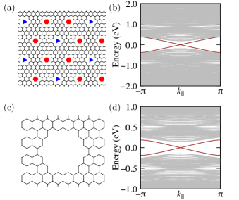
One can choose length scales for generating graphene patchwork with topological interface states. For instance, let us investigate the case of for the scaling process [Fig. 4(a)]. In the second gap-opening step, one obtains two superstructures with honeycomb and triangular hole arrays where band gaps are open at point. As can be read from Table 1, in valence bands one has for honeycomb hole array at point, whereas at M point, characterizing a topological state, while for triangular hole array at both and M points, specifying a trivial state. Because the superstructures of honeycomb and triangular hole arrays are distinct in topology, the graphene patchwork composed from them carry topological interface states as displayed explicitly in Fig. 4(b). We also investigate other holes for superstructuring, noticing that more types of hole are available for choice when large unit cells are considered, and hole shapes may affect electronic states Yu et al. (2008). As an example, we consider the case where in order to form a hole 24 carbon atoms are removed [see Fig. 4(c)]. Figures 4(d) shows the band structure of the corresponding graphene patchwork with counterpropagating interface modes. All these observations demonstrate the power of the scaling & gap-opening strategy.
Triangular hole arrays of with induce a corner-to-center BZ folding from the pristine graphene, and open a band gap at point. For the case of , we find in valence bands at point, whereas at M point. However, this choice of cannot be used for implementing graphene patchwork, since honeycomb and triangular hole arrays are not topologically distinct, i.e., the former has at point and at M point, while the latter has at point, and at M point and thus no interface state is topologically guaranteed.
The scaling & gap-opening strategy allows us to design the topological phase in a large variety of length scale. A smaller superstructure yields a larger topological gap, which is advantageous in stability of the topological phase. However, one should keep it in mind that as the superstructure gets smaller, experimental implementations become more difficult. The small structures might be fabricated by bottom up methods, i.e., polymerizing appropriate molecules, but in practice, one has to figure out an optimal length scale to fabricate the graphene patchwork, and to compose a device utilizing the interface currents with topological protection.
To summarize, we have demonstrated the generation of topological currents at the domain wall between two regions of graphene with different types of hole arrays, i.e., honeycomb and triangular. We have proposed a theoretical framework, scaling & gap-opening strategy to show the essence of the underlying physics, which can work as a guideline for exploration of new material phases by nano-structuring. While we have concentrated on perforation in graphene, chemical doping and passivation achieve the same goal. With the geometry effect playing the crucial role in our approach, the present idea applies for bosonic systems, such as photons and phonons, as well as other wave systems. The combination of topological physics and nanotechnology is expected to open a new era of fundamental and applied material science.
Acknowledgments
Acknowledgements.
TK and XH thank H. Aoki and F. Liu for useful comments and discussions. This work was supported partially by the WPI Initiative on Materials Nanoarchitectonics, Ministry of Education, Cultures, Sports, Science and Technology, Japan, and partially by JSPS KAKENHI Grant Numbers JP17K14358 and JP17H02913. TK thanks the Supercomputer Center, the Institute for Solid State Physics, the University of Tokyo for the use of the facilities.Appendix
Band structures such as those shown in Fig. 2, the left column in Fig. 3 and Fig. 4 are obtained by diagonalizing numerically the hamiltonian based on the tight-binding model. For the right panel of Fig. 2, stripes of infinite length in direction are put periodically in direction with width for both regions of honeycomb and triangular hole arrays. For Fig. 4(b) and (d), the width is taken as and , respectively. Reflecting the symmetry of the system under consideration, the eigen wave functions at and M points in the Brillouin zone can be classified by even or odd parity against the 2D spatial inversion, or equivalently rotation, with the rotation center at the blue (triangle) mark in Fig. 1(f), which are used to specify the band topology.
DFT calculations for band structures shown in Fig. 3 are performed using Vienna ab initio simulation package (VASP) Kresse and Hafner (1993, 1994); Kresse and Furthmüller (1996, 1996) with Perdew-Becke-Erzenhof (PBE) type generalized gradient approximation (GGA) for exchange correlation potential Perdew et al. (1996). The kinetic cutoff energies for the plane wave basis set used to expand the Kohn-Sham orbitals are 520 eV for the self-consistent energy calculations. 881 -point meshes are used, which is sufficient to ensure good convergence in the total energy differences. The structural relaxations are performed ensuring that the Hellmann-Feynman forces acting on ions were less than 10-3 eV/Å.
References
- Esaki and Tsu (1970) L. Esaki and R. Tsu, IBM J. Res. Dev. 14, 61 (1970).
- Novoselov et al. (2005) K. S. Novoselov, A. K. Geim, S. V. Morozov, D. Jiang, M. I. Katsnelson, I. V. Grigorieva, S. V. Dubonos, and A. A. Firsov, Nature 438, 197 (2005).
- Geim and Novoselov (2007) A. K. Geim and K. S. Novoselov, Nat Mater 6, 183 (2007).
- Castro Neto et al. (2009) A. H. Castro Neto, F. Guinea, N. M. R. Peres, K. S. Novoselov, and A. K. Geim, Rev. Mod. Phys. 81, 109 (2009).
- Park et al. (2008a) C.-H. Park, L. Yang, Y.-W. Son, M. L. Cohen, and S. G. Louie, Nature Physics 4, 213 EP (2008a).
- Park et al. (2008b) C.-H. Park, L. Yang, Y.-W. Son, M. L. Cohen, and S. G. Louie, Phys. Rev. Lett. 101, 126804 (2008b).
- Guinea et al. (2010) F. Guinea, M. I. Katsnelson, and A. K. Geim, Nat. Phys. 6, 30 (2010).
- Shima and Aoki (1993) N. Shima and H. Aoki, Phys. Rev. Lett. 71, 4389 (1993).
- Pedersen et al. (2008) T. G. Pedersen, C. Flindt, J. Pedersen, N. A. Mortensen, A.-P. Jauho, and K. Pedersen, Phys. Rev. Lett. 100, 136804 (2008).
- Sinitskii and Tour (2010) A. Sinitskii and J. M. Tour, J. Am. Chem. Soc. 132, 14730 (2010).
- Bai et al. (2010) J. Bai, X. Zhong, S. Jiang, Y. Huang, and X. Duan, Nat Nano 5, 190 (2010).
- Zhu et al. (2014) X. Zhu, W. Wang, W. Yan, M. B. Larsen, P. Bøggild, T. G. Pedersen, S. Xiao, J. Zi, and N. A. Mortensen, Nano Letters 14, 2907 (2014).
- Liu et al. (2014) L. Liu, S. Tian, Y. Long, W. Li, H. Yang, J. Li, and C. Gu, Vacuum 105, 21 (2014).
- Kazemi et al. (2015) A. Kazemi, X. He, S. Alaie, J. Ghasemi, N. M. Dawson, F. Cavallo, T. G. Habteyes, S. R. J. Brueck, and S. Krishna, Sci. Rep. 5, 11463 EP (2015).
- Sandner et al. (2015) A. Sandner, T. Preis, C. Schell, P. Giudici, K. Watanabe, T. Taniguchi, D. Weiss, and J. Eroms, Nano Letters 15, 8402 (2015).
- Gao et al. (2017) F. Gao, F. Liu, Z. Ye, C. Sui, B. Yan, P. Cai, B. Lv, Y. Li, N. Chen, Y. Zheng, and Y. Shi, Nanotechnology 28, 045304 (2017).
- Fürst et al. (2009) J. A. Fürst, J. G. Pedersen, C. Flindt, N. A. Mortensen, M. Brandbyge, T. G. Pedersen, and A.-P. Jauho, New J. Phys. 11, 095020 (2009).
- Guinea and Low (2010) F. Guinea and T. Low, Philosophical Transactions of the Royal Society of London A: Mathematical, Physical and Engineering Sciences 368, 5391 (2010).
- Petersen et al. (2011) R. Petersen, T. G. Pedersen, and A.-P. Jauho, ACS Nano 5, 523 (2011).
- Baskin and Král (2011) A. Baskin and P. Král, Sci. Rep. 1, 36 EP (2011).
- Cui et al. (2011) X. Y. Cui, R. K. Zheng, Z. W. Liu, L. Li, B. Delley, C. Stampfl, and S. P. Ringer, Phys. Rev. B 84, 125410 (2011).
- Oswald and Wu (2012) W. Oswald and Z. Wu, Phys. Rev. B 85, 115431 (2012).
- Liu et al. (2013) X. Liu, Z. Zhang, and W. Guo, Small 9, 1405 (2013).
- Dvorak et al. (2013) M. Dvorak, W. Oswald, and Z. Wu, Sci. Rep. 3, 2289 EP (2013).
- Ouyang et al. (2014) F. Ouyang, S. Peng, Z. Yang, Y. Chen, H. Zou, and X. Xiong, Phys. Chem. Chem. Phys. 16, 20524 (2014).
- Haldane (1988) F. D. M. Haldane, Phys. Rev. Lett. 61, 2015 (1988).
- Weng et al. (2015) H. Weng, R. Yu, X. Hu, X. Dai, and Z. Fang, Adv. Phys. 64, 227 (2015).
- Kane and Mele (2005a) C. L. Kane and E. J. Mele, Phys. Rev. Lett. 95, 146802 (2005a).
- Kane and Mele (2005b) C. L. Kane and E. J. Mele, Phys. Rev. Lett. 95, 226801 (2005b).
- Wu and Hu (2016) L.-H. Wu and X. Hu, Sci. Rep. 6, 24347 (2016).
- Kariyado and Hu (2017) T. Kariyado and X. Hu, Sci. Rep. 7, 16515 (2017).
- Fu (2011) L. Fu, Phys. Rev. Lett. 106, 106802 (2011).
- Chiu et al. (2016) C.-K. Chiu, J. C. Y. Teo, A. P. Schnyder, and S. Ryu, Rev. Mod. Phys. 88, 035005 (2016).
- Sushkov and Castro Neto (2013) O. P. Sushkov and A. H. Castro Neto, Phys. Rev. Lett. 110, 186601 (2013).
- Wang et al. (2017) S. Wang, D. Scarabelli, L. Du, Y. Y. Kuznetsova, L. N. Pfeiffer, K. W. West, G. C. Gardner, M. J. Manfra, V. Pellegrini, S. J. Wind, and A. Pinczuk, Nature Nanotechnology (2017), 10.1038/s41565-017-0006-x.
- Jin et al. (2017) K.-H. Jin, S.-H. Jhi, and F. Liu, Nanoscale 9, 16638 (2017).
- Cao et al. (2017) T. Cao, F. Zhao, and S. G. Louie, Phys. Rev. Lett. 119, 076401 (2017).
- Castro Neto and Guinea (2007) A. H. Castro Neto and F. Guinea, Phys. Rev. B 75, 045404 (2007).
- Liu et al. (2009) W. Liu, Z. F. Wang, Q. W. Shi, J. Yang, and F. Liu, Phys. Rev. B 80, 233405 (2009).
- Ouyang et al. (2011) F. Ouyang, S. Peng, Z. Liu, and Z. Liu, ACS Nano 5, 4023 (2011).
- Lee et al. (2013) J. Lee, A. K. Roy, J. L. Wohlwend, V. Varshney, J. B. Ferguson, W. C. Mitchel, and B. L. Farmer, Appl. Phys. Lett. 102, 203107 (2013).
- Po et al. (2017) H. C. Po, A. Vishwanath, and H. Watanabe, Nature Commun. 8, 50 (2017).
- Bradlyn et al. (2017) B. Bradlyn, L. Elcoro, J. Cano, M. G. Vergniory, Z. Wang, C. Felser, M. I. Aroyo, and B. A. Bernevig, Nature 547, 298 (2017).
- (44) J. Kruthoff, J. de Boer, J. van Wezel, C. L. Kane, and R.-J. Slager, arXiv:1612.02007 .
- (45) J. Noh, W. A. Benalcazar, S. Huang, M. J. Collins, K. Chen, T. L. Hughes, and M. C. Rechtsman, arXiv:1611.02373 .
- Tang et al. (2017) G. P. Tang, Z. H. Zhang, X. Q. Deng, Z. Q. Fan, H. Zhang, and L. Sun, RSC Adv. 7, 8927 (2017).
- Yu et al. (2008) D. Yu, E. M. Lupton, M. Liu, W. Liu, and F. Liu, Nano Research 1, 56 (2008).
- Kresse and Hafner (1993) G. Kresse and J. Hafner, Phys. Rev. B 47, 558 (1993).
- Kresse and Hafner (1994) G. Kresse and J. Hafner, Phys. Rev. B 49, 14251 (1994).
- Kresse and Furthmüller (1996) G. Kresse and J. Furthmüller, Computational Materials Science 6, 15 (1996).
- Kresse and Furthmüller (1996) G. Kresse and J. Furthmüller, Phys. Rev. B 54, 11169 (1996).
- Perdew et al. (1996) J. P. Perdew, K. Burke, and M. Ernzerhof, Phys. Rev. Lett. 77, 3865 (1996).