Electrically tunable exchange splitting in bilayer graphene on monolayer Cr2X2Te6 with X=Ge, Si, and Sn.
Abstract
We investigate the electronic band structure and the proximity exchange effect in bilayer graphene on a family of ferromagnetic multilayers Cr2X2Te6, X=Ge, Si, and Sn, with first principles methods. In each case the intrinsic electric field of the heterostructure induces an orbital gap on the order of 10 meV in the graphene bilayer. The proximity exchange is strongly band dependent. For example, in the case of Cr2Ge2Te6, the low-energy valence band of bilayer graphene has exchange splitting of 8 meV, while the low energy conduction band’s splitting is 30 times less (0.3 meV). This striking discrepancy stems from the layer-dependent hybridization with the ferromagnetic substrate. Remarkably, applying a vertical electric field of a few V/nm reverses the exchange, allowing us to effectively turn ON and OFF proximity magnetism in bilayer graphene. Such a field-effect should be generic for van der Waals bilayers on ferromagnetic insulators, opening new possibilities for spin-based devices.
Keywords: spintronics, graphene, heterostructures, proximity exchange
1 Introduction
The properties of two-dimensional materials can be strongly altered by proximity effects in van der Waals heterostructures. One prominent example is graphene, which experiences strong proximity spin-orbit coupling (SOC) effects when placed on transition metal dichalcogenides (TMDC) [1, 2], and a giant field-effect SOC when bilayer graphene is used [3]. Typical experimental structures like graphene/hBN/ferromagnet, showing very efficient spin injection [4, 5, 6, 7, 8], also feature significant proximity exchange [9, 10]. These heterostructures are presently used in optospintronic devices [1, 11, 12] and also for spin transport [5, 8, 4, 7, 6] in graphene spintronics [13]. However, when it comes to device realizations, bilayer graphene (BLG) offers many advantages, due to the possibility of having an electrically tunable band gap [14, 15], as well as the more precise control of the chemical potential [16, 17].
Graphene is a diamagnet. Can we make it “ferromagnetic” so that it could be used for spintronics applications [18, 19]? It turns out that an effective way to achieve this is to place graphene on a ferromagnetic substrate (insulator or semiconductor, to preserve the Dirac character of the bands and avoid substrate transport). Graphene then experiences proximity exchange coupling, typically in the range of meV [9, 10, 20, 21, 22, 23, 24, 25, 26, 27, 28, 29], sometimes reaching even higher values [30, 31, 32, 33]. Exchange proximity effects in graphene were observed by quantum anomalous Hall effect [20], magnetoresistance [22] and nonlocal spin transport experiments [21], as has been confirmed theoretically [26, 27, 28, 29, 30, 33].
Several ferromagnetic insulators (FMI), like EuO and Yttrium-Iron-Garnet, have been considered in the context of graphene spintronics [31, 22, 33, 32, 34]. However transition-metal trichalcogenides Cr2Si2Te6, Cr2Ge2Te6 (CGT), and transition-metal trihalides CrI3, and their monolayers are now extensively discussed in literature as promising materials for low-dimensional spintronics because of their FMI ground state properties [35, 36, 37, 38, 39, 40, 41, 42, 43, 44, 45, 46, 47, 48, 49, 50, 51, 52, 53]. These materials have attracted attention as substrates for topological insulators (TI) [49, 50] and graphene [27], because ferromagnetic coupling is present. For example, CGT seems to be a nice platform for large scale epitaxial growth of TIs with high quality interfaces, where the interaction of TI surface states and ferromagnetism can be studied [49, 50]. Moreover, first principles calculations show that monolayer graphene on CGT [27] features exchange splitting of about meV. It is then natural to try to use them for proximity effects in BLG.
For device operations, it is desirable to have electric control of the band structure and spin properties. We already know that BLG on a substrate can open a gap (similarly to having a vertical electric field applied). Could we also control exchange coupling in a similar way, simply applying an electric field? One naturally expects that the proximity effect is strongest in the BLG layer adjacent to the ferromagnetic substrate. Orbitals from this layer form, say, the valence band, which will exhibit strong exchange splitting. The conduction band, on the other hand, would have no or only weak splitting. If an electric field is applied, the situation can be reversed, and now it would be the conduction band that has the largest exchange splitting. It has also been shown in model calculations, that BLG on a FMI can be a platform for field-effect magnetic or spin devices [54, 55, 56, 57, 58]. The combination of exchange and electric field leads to the control of the spin-dependent gap of the carriers and perfect switching of the spin polarization is predicted [56, 57]. How realistic is such an electrical control of proximity exchange splitting in BLG on real magnetic substrates? We answer this question by performing DFT calculations of BLG on monolayer Cr2Si2Te6, CGT, and Cr2Sn2Te6. Indeed, we show that the exchange splitting in a given band can be switched ON and OFF by a relatively modest vertical electric field. This opens venues for investigating magnetotransport in BLG, as well as for controlling the synthetic magnetism by gates. The analogy with spin-orbit valve effect [3] is certainly there. But the exchange valve is fundamentally different, in that it generates a magnetic moment in BLG, splits the two valleys equally, and opens up a new platform for magnetotransport phenomena and spin filtering. There are now recent experiments demonstrating an electric field control of ferromagnetism in 2D ferromagnets (such as CrI3 [59] and CGT [60]). Controlling “synthetic” magnetism in BLG on such materials would be a great achievement.
In this paper we investigate, by performing first principles calculations, the proximity induced exchange coupling in BLG on monolayer CGT, as well as on Cr2Si2Te6 and Cr2Sn2Te6 (the last has been theoretically predicted [61] but not yet prepared experimentally). We find that the low energy bands of BLG show an indirect band gap of roughly meV, which can be efficiently tuned by experimentally accessible electric fields of a few V/nm. The proximity induced exchange splitting of the valence band is giant, being around meV, -times larger than the exchange splitting in the conduction band. This large difference arises from the fact, that the valence band is formed by non-dimer carbon atoms from the bottom graphene layer directly above CGT, where the proximity effect is strong, while the conduction band is formed by non-dimer carbon atoms from the top graphene layer, where the proximity effect is weak (in BLG with Bernal stacking, one pair of carbon atoms is vertically connected, which we call dimer, the other pair non-dimer). The most interesting result is the switching of the exchange splitting from the valence to the conduction band, via an external electric field that counters the built-in field of the BLG/CGT heterostructure. A proximity exchange valve is realized. We also include a brief discussion on possible device geometries based on the field-effect proximity exchange.
2 Computational details and geometry
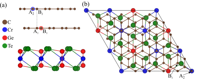
The heterostructure of BLG on CGT is shown in Fig. 1, where a supercell of BLG is placed on a CGT supercell. The considered heterostructure model contains 130 atoms in the unit cell. We keep the lattice constant of graphene unchanged at Å and stretch the lattice constant of CGT by roughly 4% from Å [36] to Å. Theoretical calculations predict that the tensile strain leaves the ferromagnetic ground state unchanged, but enhances the band gap and the Curie temperature of CGT [46, 43]. In Fig. 1(a) the side view of the structure shows the Bernal stacking of BLG, with an average distance relaxed to Å between the graphene layers, in good agreement with experiment [62]. The average distance between the lower graphene layer and CGT was relaxed to Å, consistent with literature [27].
Previous calculations show that the relative alignment of graphene on CGT does not influence the electronic bands much, see Ref. [27], and we will only consider the supercell with stacking as in Fig. 1. We will also not consider SOC in the calculation, since it was shown that proximity induced exchange in graphene, caused by CGT, is one order of magnitude larger than proximity SOC [27]. The electronic structure calculations and structural relaxation of BLG on CGT were performed by means of density functional theory (DFT) [63] within Quantum ESPRESSO [64]. Self-consistent calculations were performed with the -point sampling of to get converged results for the proximity exchange splittings. We have performed open shell calculations that provide the spin polarized ground state with a collinear magnetization. Theory and experiment predict that CGT is a FMI with magnetic anisotropy favoring a magnetization perpendicular to the CGT-plane [40, 37, 61, 35, 36, 38, 50, 39]. A Hubbard parameter of eV was used for Cr -orbitals, being in the range of proposed values especially for this compound [39]. The value results from comparison of DFT and experiment on the magnetic ground state of bulk CGT. Other theoretical calculations report, that their results are qualitatively independent from the used values [46, 45]. We used an energy cutoff for charge density of Ry, and the kinetic energy cutoff for wavefunctions was Ry for the scalar relativistic pseudopotential with the projector augmented wave method [65] with the Perdew-Burke-Ernzerhof exchange correlation functional [66]. For the relaxation of the heterostructures, we added van-der-Waals corrections [67, 68] and used quasi-newton algorithm based on trust radius procedure. In order to simulate quasi-2D systems the vacuum of Å was used to avoid interactions between periodic images in our slab geometry. Dipole corrections [69] were also included to get correct band offsets and internal electric fields. To determine the interlayer distances, the atoms of BLG were allowed to relax only in their positions (vertical to the layers), and the atoms of CGT were allowed to move in all directions, until all components of all forces were reduced below [Ry/], where is the Bohr radius.
3 Electronic band structure of BLG on CGT.
The electronic structure of bare BLG contains four parabolic bands near the Fermi energy [70, 71]. Two low energy bands close to the charge neutrality point are formed by () orbitals of non-dimer atoms B1 and A2, see Fig. 1. In addition, there are two higher lying bands formed by the orbitals of dimer atoms A1 and B2, see Fig. 1. Since the dimer atoms are connected by direct interlayer hopping, the bands are shifted roughly 400 meV from the Fermi level, such that they can be ignored for transport.
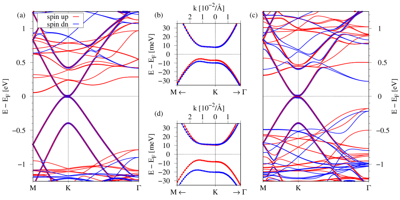
In Fig. 2(a) we show the calculated electronic band structure of BLG on monolayer CGT along high symmetry lines. The bands near the Fermi level resemble closely the bands from bare BLG [70, 71], even though the high energy conduction band of BLG is located within the conduction bands of CGT. Very important for transport is that the low energy bands of BLG are located within the band gap of CGT. The offset between the conduction band of BLG at K and the bottom of conduction band minimum of CGT is roughly meV.
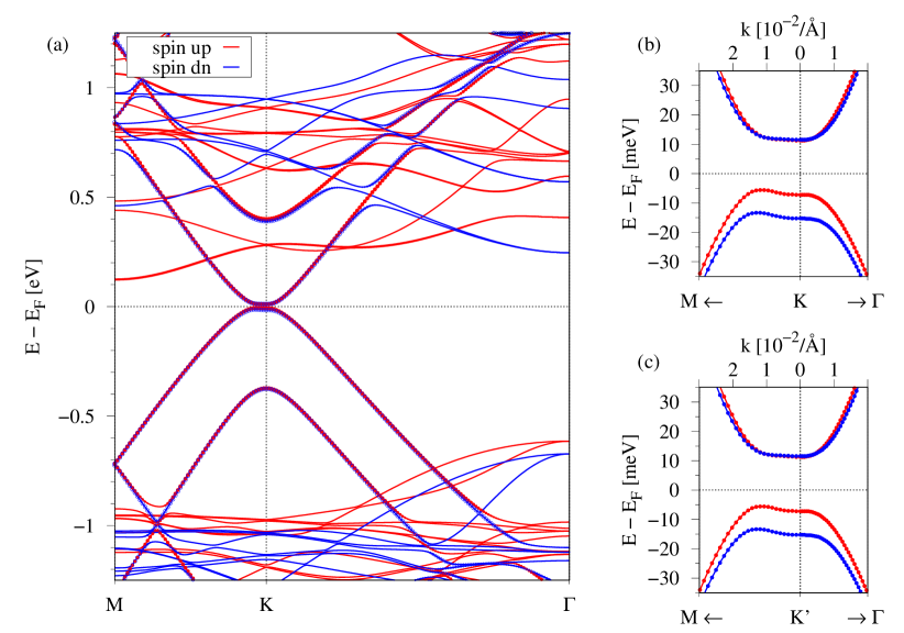
However, there are two important differences compared to bare BLG. First, the heterostructure possesses an intrinsic dipole (vertical to the sheets) and thus the two graphene layers are at a different potential energy resulting in a small indirect orbital gap of roughly meV, see Fig. 2(b). The dipole of Debye points from CGT towards BLG and therefore B1 (A2) electrons have lower (higher) energy forming the valence (conduction) states. Second, the ferromagnetic CGT substrate interacts mainly with the lower graphene layer and, by proximity exchange, splits the low energy bands originating from this graphene layer by meV, see Fig. 2(b). The upper graphene layer is far away and experiences almost no proximity effect, resulting in a comparatively small spin splitting of the corresponding bands. The calculated magnetic moment of the Cr-atoms is positive and roughly , but the Te-atoms and consequently the C-atoms are polarized with a small negative magnetic moment. Thus the BLG low energy valence band is spin split, with spin down states being lower in energy, see Fig. 2(b). We would also like to emphasize, that due to the ferromagnetic substrate we break time-reversal symmetry. Thus the band structure and also the splitting is the same for K and K’ point, see Fig. 2(b,c). This is in contrast to proximity SOC in BLG on WSe2 [3], where K and K’ point are connected by time-reversal symmetry.
4 Proximity exchange valve
In order to design devices for spintronics it is desirable if one can electrically control both spin and orbital properties. Such a control should be highly efficient in our heterostructures. In Fig. 3 we show the low energy band structures of BLG, in the presence of a vertical electric field. At zero field strength, see Fig. 3(c), the situation is as explained above; the hole band formed by -orbitals of B1 is strongly split by proximity exchange, while the electron band, formed by -orbitals of A2 is much less split. The reason is simply because the atoms B1 are closer to the ferromagnetic substrate experiencing a stronger proximity effect than atoms A2. The ordering of the bands is determined by the built-in electric field, pointing from CGT towards BLG, and thus B1 electrons are at lower energy.
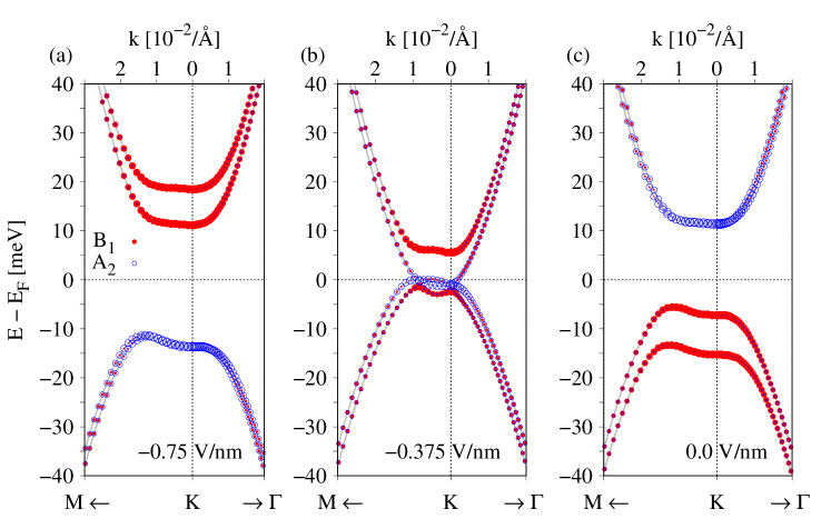
Now, if we apply a positive external electric field, it adds to the internal field, opening the orbital gap further, keeping the band-dependent exchange splitting unchanged. But when the applied field is negative and strong enough to compensate the built-in electric field, the orbital gap closes, see Fig. 3(b). This compensation happens at roughly V/nm and the states from atoms B1 and A2 are almost at the same potential energy, closing the gap.
A further increase of the negative field leads to the reopening of the band gap, see Fig. 3(a), but with a switched character of the bands. Now, the conduction band is formed by atoms B1, which still experience the stronger proximity effect, while the valence band is formed by atoms A2, which are far from the ferromagnetic substrate. The switching of the band character happens, because the total (external and built-in) field is pointing now from BLG towards CGT, opposite to the zero-field case. Thus, atoms B1 experience a higher potential than atoms A2. We get a proximity exchange valve.
Are the relevant BLG low-energy bands still within the orbital band gap of CGT? In Fig. 4(a), we see that the calculated dipole depends linearly on the applied electric field. The built-in dipole is roughly compensated by an external field of V/nm; the amplitude of the intrinsic field is V/nm. Figure 4(a) also shows that the energy offset between the BLG conduction band at K and the bottom of the conduction band minimum of CGT also changes with electric field. However, it is important to note that the low energy states of BLG are located within the band gap of CGT for electric fields that allow to observe the proximity exchange switching of the states. For fields larger than V/nm, the conduction band of BLG at K is shifted above the bottom of the conduction band minimum of CGT and BLG gets hole doped.
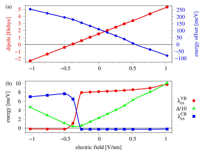
In Fig. 4(b), we show the evolution of the exchange splittings and the orbital gap as a function of the applied electric field. For this we define the orbital gap , as the average of the spin up () and spin down () orbital gaps, at the K point. The exchange splitting is defined as the energy difference between spin up and spin down band, , at the K point for conduction band (CB) and valence band (VB) respectively. The orbital gap, which is a measure for the strength of the intrinsic dipole across the junction, is consistent with our dipole values. In Fig. 4(b), we see that the gap has its minimum value, when the applied field compensates the intrinsic dipole, at around V/nm. If we look at the two splitting parameters and , we can see that there is a very nice switching behavior around V/nm, where the gap has its minimum. The conduction band splitting is around meV for fields smaller than V/nm and then drops to a small negative value when applying a larger field strength. The opposite behavior is observed for the valence band splitting , which has a large magnitude for fields larger than V/nm, see Fig. 4(b). We find that the switching happens within a few hundred millivolts per nanometer, and most important at experimentally accessible field strengths.
5 BLG on Cr2Si2Te6 and Cr2Sn2Te6
We predict similar scenarios for X=Si and Sn. In Fig. 5 we show the band structure of BLG on Cr2Si2Te6 and Cr2Sn2Te6. Very similar to the bands of BLG on CGT, we see proximity spin splitting in the low energy valence band, much larger than in the conduction band. Here we would like to mention that the compounds with Si and Ge have been identified in experiments [35, 36], whereas the compound with Sn atoms has been only predicted theoretically [61] so far.
In the Si (Sn) case, proximity induced exchange is smaller (larger), as the valence band spin splitting is about meV ( meV) at the K point and the indirect gap is roughly meV ( meV). The energy offset between the conduction band of BLG at K and the bottom of conduction band minimum of Cr2Si2Te6 (Cr2Sn2Te6) is roughly meV ( meV). The intrinsic dipole is weaker (stronger), about () Debye, which in the end leads to slightly different electric fields to observe the switching of the band character, as shown for BLG on CGT. The average distance between the lower graphene layer and Cr2Si2Te6 (Cr2Sn2Te6) was relaxed to () Å. From the minimal difference in distance, we conclude that the spin splitting strongly depends on the material itself, whereas in Ref. [27], it was already shown that proximity induced exchange splitting strongly depends on the distance between graphene and the CGT substrate.
For model transport calculations it is useful to have realistic parameters in order to estimate the conductance through BLG in this heterostructures. In Tab. 1 we summarize the most relevant parameters for bilayer graphene on all three considered substrates, for zero applied external field. The exchange splitting of the valence band is always roughly times larger than the splitting of the conduction band, independent of the material. Note that has the opposite sign of , see Tab. 1, meaning that the order of the spin bands for conduction band is different from the valence band, at the K point.
6 Bilayer graphene device
The electrical switching of the exchange splitting is a nice platform to realize novel spintronics devices, particularly since high spin-polarization can be achieved. Indeed, without any applied field, the chemical potential can be tuned close to the maximum of the valence band where states are 100% spin polarized. The same would hold for the conduction band in an applied negative field. Based on theoretical model calculations — on magnetoresistance in BLG [72] and spin transport in graphene [29, 73], both being subject to proximity exchange — model transport calculations in FMI/BLG were performed [54, 55]. It was found that the proximity induced spin splitting allows BLG to act as a spin filter and spin rotator, being electrically controllable.
In Fig. 6 we show the structure of a spin filter, where BLG is deposited on an insulating substrate. On top of BLG we have two regions where CGT is placed, but in principle also other FMIs (YIG, EuO, CrI3) are possible candidates to realize the following devices. On top of the regions with the FMIs, gate voltages and can be applied. The magnetization directions of the two FMIs are opposite.
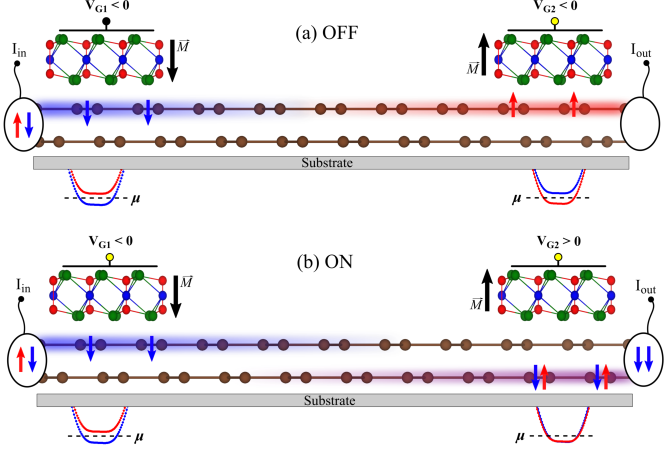
Suppose the gate voltage is negative, then the low energy conduction bands of BLG below that first FMI are formed by the upper graphene layer and are strongly spin split, see Fig. 6(a). A spin unpolarized current is injected from the left and enters the first heterostructure. If the chemical potential is between the two spin split electron bands, one spin component is filtered. In the central part we have just bare BLG where, due to small intrinsic SOC, the spin keeps its direction aligned until it enters the second heterostructure. Depending on the gate voltage , we can have a ON or an OFF state. Since the magnetization of the second FMI is opposite to the first one the electrons cannot travel on in the upper layer if is also negative, because only the opposite spin channel is open, see Fig. 6(a). However, if is positive, the conduction bands are formed by the lower graphene layer, having almost no proximity exchange, and the electrons have both spin channels open, see Fig. 6(b).
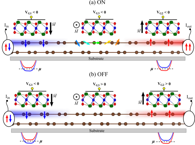
A different approach is based on the spin rotation, see Fig. 7. Similar to the spin filter, we polarize first a spin unpolarized current injected from the left, which is then analyzed in the right heterostructure. The difference is that there is an additional FMI able to control the carrier spins via gate voltage . The magnetization directions of the FMIs from left to right are and spin rotation happens below the central FMI. Depending on the gate voltage , carriers will flip their spin in the central region and the channel on the right is open, see Fig. 7(a), or closed, see Fig. 7(b). The origin of spin rotation and the efficiency of this device has been discussed in Refs. [54, 55], and is based on wave function localization and short ranged proximity exchange.
Above are but a few examples of spin devices based on the field-effect exchange coupling concepts. BLG on ferromagnetic insulating substrates could be employed to build bipolar spintronics elements, such as spin diodes and spin transistors [74] or spin logic devices [75], which require exchange coupling (but non necessarily magnetic moments) to make their electronic bands spin dependent.
7 Summary and Conclusion
In conclusion, we have studied from first principles the electronic structure of bilayer graphene on Cr2Ge2Te6. We have shown that we can efficiently, and most important fully electrically, switch the exchange interaction by one order of magnitude, of electrons and holes. At low enough energy the electronic states can be 100% spin polarized, which can lead to interesting new device concepts. We also expect that our DFT-derived parameters will be useful in model transport calculations involving exchange proximitized BLG.
Acknowledgments
This work was supported by DFG SPP 1666, SFB 689, SFB 1277 (A09 and B07), and by the European
Unions Horizon 2020 research and innovation
programme under Grant agreement No. 696656.
The authors gratefully acknowledge the Gauss Center for Supercomputing e.V.
for providing computational resources on the GCS Supercomputer SuperMUC at Leibniz Supercomputing Center.
References
References
- [1] Gmitra M and Fabian J 2015 Phys. Rev. B 92(15) 155403 URL https://link.aps.org/doi/10.1103/PhysRevB.92.155403
- [2] Gmitra M, Kochan D, Högl P and Fabian J 2016 Phys. Rev. B 93(15) 155104 URL https://link.aps.org/doi/10.1103/PhysRevB.93.155104
- [3] Gmitra M and Fabian J 2017 Phys. Rev. Lett. 119(14) 146401 URL https://link.aps.org/doi/10.1103/PhysRevLett.119.146401
- [4] Gurram M, Omar S and van Wees B J 2017 Nat. Commun. 8 248 URL http://www.nature.com/articles/s41467-017-00317-w
- [5] Kamalakar M V, Dankert A, Bergsten J, Ive T and Dash S P 2014 Sci. Rep. 4 6146 URL https://www.nature.com/articles/srep06146
- [6] Yamaguchi T, Inoue Y, Masubuchi S, Morikawa S, Onuki M, Watanabe K, Taniguchi T, Moriya R and Machida T 2013 Appl. Phys. Express 6 073001 URL http://iopscience.iop.org/article/10.7567/APEX.6.073001/meta
- [7] Kamalakar M V, Dankert A, Kelly P J and Dash S P 2016 Sci. Rep. 6 21168 URL https://www.nature.com/articles/srep21168
- [8] Fu W, Makk P, Maurand R, Bräuninger M and Schönenberger C 2014 J. Appl. Phys. 116 074306 URL http://aip.scitation.org/doi/10.1063/1.4893578
- [9] Zollner K, Gmitra M, Frank T and Fabian J 2016 Phys. Rev. B 94(15) 155441 URL https://link.aps.org/doi/10.1103/PhysRevB.94.155441
- [10] Lazić P, Belashchenko K D and Žutić I 2016 Phys. Rev. B 93(24) 241401 URL https://link.aps.org/doi/10.1103/PhysRevB.93.241401
- [11] Avsar A, Unuchek D, Liu J, Sanchez O L, Watanabe K, Taniguchi T, Özyilmaz B and Kis A 2017 ACS Nano 11 11678–11686 ISSN 1936-0851 URL http://arxiv.org/abs/1705.10267http://pubs.acs.org/doi/10.1021/acsnano.7b06800
- [12] Luo Y K, Xu J, Zhu T, Wu G, McCormick E J, Zhan W, Neupane M R and Kawakami R K 2017 Nano Lett. 17 3877–3883
- [13] Han W, Kawakami R K, Gmitra M and Fabian J 2014 Nat. Nano. 9 794–807 URL http://dx.doi.org/10.1038/nnano.2014.214
- [14] Zhang Y, Tang T T, Girit C, Hao Z, Martin M C, Zettl A, Crommie M F, Shen Y R and Wang F 2009 Nature 459 820–823 ISSN 0028-0836 URL http://www.nature.com/doifinder/10.1038/nature08105
- [15] Oostinga J B, Heersche H B, Liu X, Morpurgo A F and Vandersypen L M K 2008 Nat. Mater. 7 151–157 URL http://www.nature.com/doifinder/10.1038/nmat2082
- [16] Martin J, Akerman N, Ulbricht G, Lohmann T, Smet J H, von Klitzing K and Yacoby A 2008 Nat. Phys. 4 144–148 ISSN 1745-2473 URL http://dx.doi.org/10.1038/nphys781
- [17] Rutter G M, Jung S, Klimov N N, Newell D B, Zhitenev N B and Stroscio J A 2011 Nat. Phys. 7 649–655 ISSN 1745-2473 URL http://dx.doi.org/10.1038/nphys1988
- [18] Žutić I, Fabian J and Das Sarma S 2004 Rev. Mod. Phys. 76(2) 323–410 URL https://link.aps.org/doi/10.1103/RevModPhys.76.323
- [19] Fabian J, Matos-Abiague A, Ertler C, Stano P and Žutić I 2007 Acta Phys. Slov. 57 342 URL http://arxiv.org/abs/0711.1461
- [20] Wang Z, Tang C, Sachs R, Barlas Y and Shi J 2015 Phys. Rev. Lett. 114(1) 016603 URL https://link.aps.org/doi/10.1103/PhysRevLett.114.016603
- [21] Leutenantsmeyer J C, Kaverzin A A, Wojtaszek M and van Wees B J 2016 2D Mater. 4 014001 URL http://iopscience.iop.org/article/10.1088/2053-1583/4/1/014001
- [22] Mendes J B S, Alves Santos O, Meireles L M, Lacerda R G, Vilela-Leão L H, Machado F L A, Rodríguez-Suárez R L, Azevedo A and Rezende S M 2015 Phys. Rev. Lett. 115 226601 ISSN 0031-9007 URL https://link.aps.org/doi/10.1103/PhysRevLett.115.226601
- [23] Sakai S, Majumdar S, Popov Z I, Avramov P V, Entani S, Hasegawa Y, Yamada Y, Huhtinen H, Naramoto H, Sorokin P B and Yamauchi Y 2016 ACS Nano 10 7532–7541
- [24] Swartz A G, Odenthal P M, Hao Y, Ruoff R S and Kawakami R K 2012 ACS Nano 6 10063–10069
- [25] Wei P, Lee S, Lemaitre F, Pinel L, Cutaia D, Cha W, Katmis F, Zhu Y, Heiman D, Hone J, Moodera J S and Chen C T 2016 Nat. Mater. 15 711–716 URL http://www.nature.com/doifinder/10.1038/nmat4603
- [26] Dyrdał A and Barnaś J 2017 2D Materials 4 034003 ISSN 20531583 URL http://arxiv.org/abs/1705.03220
- [27] Zhang J, Zhao B, Yao Y and Yang Z 2015 Phys. Rev. B 92(16) 165418 URL https://link.aps.org/doi/10.1103/PhysRevB.92.165418
- [28] Song Y 2018 J. Phys. D: Appl. Phys. 51 025002 ISSN 0022-3727 URL http://iopscience.iop.org/article/10.1088/1361-6463/aa9b5e
- [29] Haugen H, Huertas-Hernando D and Brataas A 2008 Phys. Rev. B 77 115406 URL http://link.aps.org/doi/10.1103/PhysRevB.77.115406
- [30] Zhang J, Zhao B, Yao Y and Yang Z 2015 Sci. Rep. 5 10629 URL http://www.nature.com/articles/srep10629
- [31] Yang H X, Hallal A, Terrade D, Waintal X, Roche S and Chshiev M 2013 Phys. Rev. Lett. 110(4) 046603 URL https://link.aps.org/doi/10.1103/PhysRevLett.110.046603
- [32] Hallal A, Ibrahim F, Yang H, Roche S and Chshiev M 2017 2D Mater. 4 025074 URL http://iopscience.iop.org/article/10.1088/2053-1583/aa6663
- [33] Su S, Barlas Y, Li J, Shi J and Lake R K 2017 Phys. Rev. B 95(7) 075418 URL https://link.aps.org/doi/10.1103/PhysRevB.95.075418
- [34] Singh S, Katoch J, Zhu T, Meng K Y, Liu T, Brangham J T, Yang F, Flatté M E and Kawakami R K 2017 Phys. Rev. Lett. 118(18) 187201 URL https://link.aps.org/doi/10.1103/PhysRevLett.118.187201
- [35] Carteaux V, Ouvrard G, Grenier J C and Laligant Y 1991 J. Magn. Magn. Mater. 94 127–133
- [36] Carteaux V, Brunet D, Ouvrard G and Andre G 1995 J. Phys.: Condens. Mat. 7 69–87 URL http://stacks.iop.org/0953-8984/7/i=1/a=008
- [37] Williams T J, Aczel A A, Lumsden M D, Nagler S E, Stone M B, Yan J Q and Mandrus D 2015 Phys. Rev. B 92(14) 144404 URL https://link.aps.org/doi/10.1103/PhysRevB.92.144404
- [38] Casto L D, Clune A J, Yokosuk M O, Musfeldt J L, Williams T J, Zhuang H L, Lin M W, Xiao K, Hennig R G, Sales B C, Yan J Q and Mandrus D 2015 APL Materials 3 041515 ISSN 2166-532X URL https://doi.org/10.1063/1.4914134
- [39] Gong C, Li L, Li Z, Ji H, Stern A, Xia Y, Cao T, Bao W, Wang C, Wang Y, Qiu Z Q, Cava R J, Louie S G, Xia J and Zhang X 2017 Nature 546 265–269 URL http://www.nature.com/doifinder/10.1038/nature22060
- [40] Zhang X, Zhao Y, Song Q, Jia S, Shi J and Han W 2016 Jpn. J. Appl. Phys. 55 033001 URL http://iopscience.iop.org/article/10.7567/JJAP.55.033001/meta
- [41] Siberchicot B, Jobic S, Carteaux V, Gressier P and Ouvrard G 1996 J. Phys. Chem. 100 5863–5867 URL http://pubs.acs.org/doi/abs/10.1021/jp952188s
- [42] Lin M W, Zhuang H L, Yan J, Ward T Z, Puretzky A A, Rouleau C M, Gai Z, Liang L, Meunier V, Sumpter B G, Ganesh P, Kent P R C, Geohegan D B, Mandrus D G and Xiao K 2016 J. Mater. Chem. C 4 315–322 URL http://xlink.rsc.org/?DOI=C5TC03463A
- [43] Chen X, Qi J and Shi D 2015 Phys. Lett. A 379 60–63 URL http://dx.doi.org/10.1016/j.physleta.2014.10.042
- [44] Liu Y and Petrovic C 2017 Phys. Rev. B 96 054406 URL http://link.aps.org/doi/10.1103/PhysRevB.96.054406
- [45] Sivadas N, Daniels M W, Swendsen R H, Okamoto S and Xiao D 2015 Phys. Rev. B 91(23) 235425 URL https://link.aps.org/doi/10.1103/PhysRevB.91.235425
- [46] Li X and Yang J 2014 Journal of Materials Chemistry C 2 7071 ISSN 2050-7526 URL http://xlink.rsc.org/?DOI=C4TC01193G
- [47] Lin G T, Zhuang H L, Luo X, Liu B J, Chen F C, Yan J, Sun Y, Zhou J, Lu W J, Tong P, Sheng Z G, Qu Z, Song W H, Zhu X B and Sun Y P 2017 Phys. Rev. B 95(24) 245212 URL https://link.aps.org/doi/10.1103/PhysRevB.95.245212
- [48] Xing W, Chen Y, Odenthal P M, Zhang X, Yuan W, Su T, Song Q, Wang T, Zhong J, Jia S, Xie X C, Li Y and Han W 2017 2D Mater. 4 024009 URL http://iopscience.iop.org/article/10.1088/2053-1583/aa7034/meta
- [49] Alegria L D, Ji H, Yao N, Clarke J J, Cava R J and Petta J R 2014 Appl. Phys. Lett. 105 053512 URL http://aip.scitation.org/doi/10.1063/1.4892353
- [50] Ji H, Stokes R A, Alegria L D, Blomberg E C, Tanatar M A, Reijnders A, Schoop L M, Liang T, Prozorov R, Burch K S, Ong N P, Petta J R and Cava R J 2013 J. Appl. Phys. 114 114907 URL http://aip.scitation.org/doi/10.1063/1.4822092
- [51] Huang B, Clark G, Navarro-Moratalla E, Klein D R, Cheng R, Seyler K L, Zhong D, Schmidgall E, McGuire M A, Cobden D H, Yao W, Xiao D, Jarillo-Herrero P and Xu X 2017 Nature 546 270–273 ISSN 0028-0836 URL http://www.nature.com/doifinder/10.1038/nature22391
- [52] Liu J, Sun Q, Kawazoe Y and Jena P 2016 Phys. Chem. Chem. Phys. 18 8777–8784 ISSN 1463-9076 URL http://xlink.rsc.org/?DOI=C5CP04835D
- [53] McGuire M 2017 Crystals 7 121 ISSN 2073-4352 URL http://dx.doi.org/10.3390/cryst7050121
- [54] Michetti P, Recher P and Iannaccone G 2010 Nano Lett. 10 4463–4469
- [55] Michetti P and Recher P 2011 Phys. Rev. B 84(12) 125438 URL https://link.aps.org/doi/10.1103/PhysRevB.84.125438
- [56] Jatiyanon K, Tang I M and Soodchomshom B 2016 Chin. Phys. B 25 078104 URL http://iopscience.iop.org/article/10.1088/1674-1056/25/7/078104/meta
- [57] Yu Y, Liang Q and Dong J 2011 Phys. Lett. A 375 2858–2862 URL http://dx.doi.org/10.1016/j.physleta.2011.06.023
- [58] Rashidian Z, Mojarabian F M, Bayati P, Rashedi G, Ueda a and Yokoyama T 2014 J. Phys.: Condens. Matter 26 255302 URL http://www.ncbi.nlm.nih.gov/pubmed/24891499
- [59] Jiang S, Li L, Wang Z, Mak K F and Shan J 2018 arXiv :1802.07355 (Preprint 1802.07355) URL http://arxiv.org/abs/1802.07355
- [60] Wang Z, Zhang T Y, Ding M, Dong B, Li Y X, Chen M L, Li X X, Li Y, Li D, Jia C K, Sun L D, Guo H, Sun D M, Chen Y S, Yang T, Zhang J, Ono S, Han Z V and Zhang Z D 2018 1–8 (Preprint 1802.06255) URL http://arxiv.org/abs/1802.06255
- [61] Zhuang H L, Xie Y, Kent P R C and Ganesh P 2015 Phys. Rev. B 92 035407 URL https://link.aps.org/doi/10.1103/PhysRevB.92.035407
- [62] Baskin Y and Meyer L 1955 Phys. Rev. 100(2) 544–544 URL https://link.aps.org/doi/10.1103/PhysRev.100.544
- [63] Hohenberg P and Kohn W 1964 Phys. Rev. 136(3B) B864–B871 URL https://link.aps.org/doi/10.1103/PhysRev.136.B864
- [64] Giannozzi P, Baroni S, Bonini N, Calandra M, Car R, Cavazzoni C, Ceresoli D, Chiarotti G L, Cococcioni M, Dabo I, Corso A D, Fabris S, Fratesi G, de Gironcoli S, Gebauer R, Gerstmann U, Gougoussis C, Kokalj A, Lazzeri M, Martin-Samos L, Marzari N, Mauri F, Mazzarello R, Paolini S, Pasquarello A, Paulatto L, Sbraccia C, Scandolo S, Sclauzero G, Seitsonen A P, Smogunov A, Umari P and Wentzcovitch R M 2009 J. Phys.: Condens. Mat. 21 395502 URL http://stacks.iop.org/0953-8984/21/i=39/a=395502
- [65] Kresse G and Joubert D 1999 Phys. Rev. B 59(3) 1758–1775 URL https://link.aps.org/doi/10.1103/PhysRevB.59.1758
- [66] Perdew J P, Burke K and Ernzerhof M 1996 Phys. Rev. Lett. 77(18) 3865–3868 URL https://link.aps.org/doi/10.1103/PhysRevLett.77.3865
- [67] Grimme S 2006 J. Comput. Chem. 27 1787–1799 ISSN 1096-987X URL http://dx.doi.org/10.1002/jcc.20495
- [68] Barone V, Casarin M, Forrer D, Pavone M, Sambi M and Vittadini A 2009 J. Comput. Chem. 30 934–939 ISSN 1096-987X URL http://dx.doi.org/10.1002/jcc.21112
- [69] Bengtsson L 1999 Phys. Rev. B 59(19) 12301–12304 URL https://link.aps.org/doi/10.1103/PhysRevB.59.12301
- [70] Nilsson J, Castro Neto A H, Guinea F and Peres N M R 2008 Phys. Rev. B 78(4) 045405 URL https://link.aps.org/doi/10.1103/PhysRevB.78.045405
- [71] McCann E and Koshino M 2013 Rep. Prog. Phys. 76 056503 URL http://stacks.iop.org/0034-4885/76/i=5/a=056503
- [72] Semenov Y G, Zavada J M and Kim K W 2008 Phys. Rev. B 77 235415 URL https://link.aps.org/doi/10.1103/PhysRevB.77.235415
- [73] Semenov Y G, Zavada J M and Kim K W 2010 J. Appl. Phys. 107 064507 URL http://aip.scitation.org/doi/10.1063/1.3354066
- [74] Zutic I, Fabian J and Erwin S C 2006 IBM J. Res. Dev. 50 121–139 ISSN 0018-8646
- [75] Behin-Aein B, Datta D, Salahuddin S and Datta S 2010 Nat. Nano. 5 266–270 ISSN 1748-3387 URL http://dx.doi.org/10.1038/nnano.2010.31