Electric-field control of magnetism in few-layered van der Waals magnet
††* These authors contribute equally.†††Corresponding to: yuansen.chen@googlemail.com, yangteng@imr.ac.cn, and vitto.han@gmail.comManipulating quantum state via electrostatic gating has been intriguing for many model systems in nanoelectronics. When it comes to the question of controlling the electron spins, more specifically, the magnetism of a system, tuning with electric field has been proven to be elusive. Recently, magnetic layered semiconductors have attracted much attention due to their emerging new physical phenomena. However, challenges still remain in the demonstration of a gate controllable magnetism based on them. Here, we show that, via ionic gating, strong field effect can be observed in few-layered semiconducting Cr2Ge2Te6 devices. At different gate doping, micro-area Kerr measurements in the studied devices demonstrate tunable magnetization loops below the Curie temperature, which is tentatively attributed to the moment re-balance in the spin-polarized band structure. Our findings of electric-field controlled magnetism in van der Waals magnets pave the way for potential applications in new generation magnetic memory storage, sensors, and spintronics.
I Introduction
The family of two-dimensional (2D) van der Waals (vdW) materials hold great promise for both fundamental physics and future applications.Geim_Roadmap ; Neto_Science One of the major characteristics of vdW materials is that, by diminishing the dimensionality into a 2D limit, Coulomb screening reduces significantly, which allows the constructions of new concept nano-electronic transistors or sensors via gate-tuning the Fermi levels of the resulted intrinsic semi-metals or semiconductors.Cory_NatNano ; SpinValve_PRL ; Duan_review ; Iwasa_Science .
Among the variety of vdW materials, layered magnetic compounds are of particular interest thanks to the enriched spin-related physics in the system.Sachs_PRB_2013 ; McGuire_CM_2015 ; Tian_2DM_2016 ; Sivadas_PRB_2015 ; McGuire_Crystals_2017 ; Lee_APLMater_2016 ; May_PRB_2016 ; Liu_SciRep_2016 ; Kurumaji_PRL_2011 ; PRL_Prediction ; NatNano_Prediction For example, the long-standing Mermin-Wagner restriction MW_Theorem has been recently lifted in the monolayer limit in CrI3, which shows Ising ferromagnetism despite of the zero out-of-plane dimensionalityXD_Xu_Nature ; Xiang_Nature . Previous studies on few-layered vdW magnets have also manifested much promising physical phenomena, including the observation of spin-resolved Raman modes,FePS_Raman_NanoLett ; FePS_Raman_2DMat the spin waves measured by neutron scattering,SpinWave_CrSiTe potential applications in spinvlaves,APL_SpinValve as well as the synthesis of new magnetic semiconductors by doping non-magnetic vdW crystals.ZhongmingWei_NC ; Fluorided_BN Recent advances in the peculiar tunnelling magneto-resistance in CrI3 further reveals that atomically thin vdW magnetic materials may serve as potential magnetic sensors.Morpurgo_CrI3 ; Pablo_CrI3 ; XiaodongXu_CrI3
However, albeit most of the vdW magnets behave as semiconductors, very few reports have been conducted on field effect transistors (FETs) based on them.CrSiTe_JMCC ; HanWei_2DMat Especially, studies that utilize the electric field as a knob to effectively tune their magnetism is thus far missing. It is known that electric-field control of magnetization is key for future applications in spintronics, e.g., spin transistors.Spin_transistor ; HideoOhno_Review To date, to reach this goal, multiple approaches have been developed, including multiferroic heterostructures, Cherifi_NM2014 thin metals,Chiba_NM2011 ; Weisheit_Science_2007 multilayered magnetic thin films,WeigangWang_NM2012 ; Maruyama_NN2009 ; SongCheng_AM2015 and diluted magnetic semiconductors.Hideo_Nature_DMS2000 ; Chiba_Science2003
In this work, we show that few-layered semiconducting Cr2Ge2Te6 devices can remain conducting and gate tunable below their ferromagnetic Curie temperature. Micro-area Kerr measurements at low temperatures were then carried out on the basis of those Cr2Ge2Te6 transistors with ionic liquid gating, which enabled tunable magnetization loops at different gate doping. The observed behavior of gate-tuned magnetism in few-layered Cr2Ge2Te6 paves the way for future spintronic applications using vdW magnet as a platform.
II Results
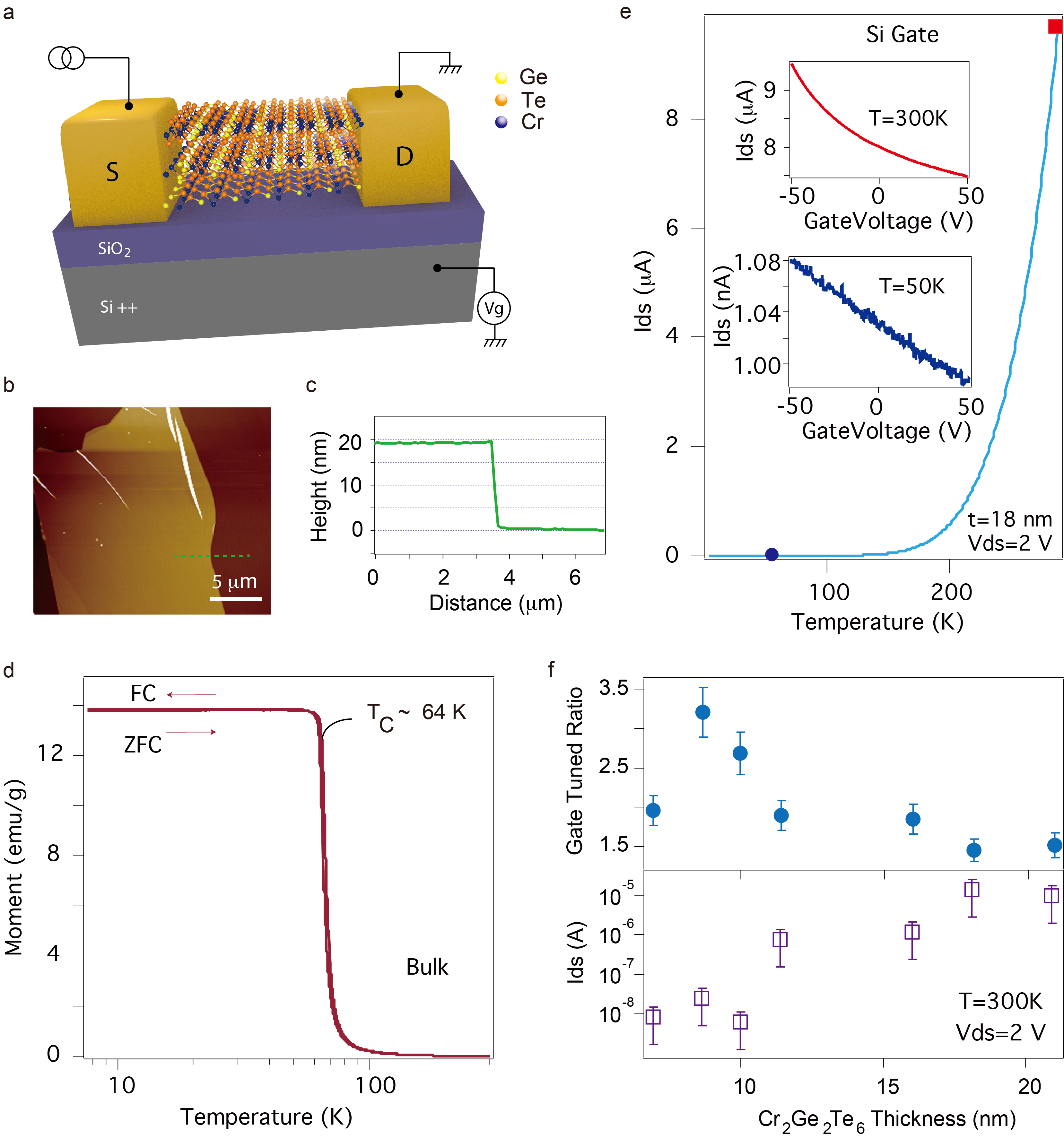
Fabrication of few-layered Cr2Ge2Te6 FETs. Single crystal Cr2Ge2Te6 was prepared via the Te self-flux method and was confirmed via x-ray diffraction (see Methods and Fig.S1 in the Suppl. Info.). We then applied the scotch tape method to exfoliate the bulk and deposited few-layered Cr2Ge2Te6 onto 285 nm thick silicon oxide grown on heavily doped silicon wafers for further FET fabrications (Fig. 1a). Atomic Force Microscope (AFM) scan of such typical flakes is shown in Figure 1 (b)–(c). Before measuring few-layered Cr2Ge2Te6, we performed zero-field-cooled (ZFC) and field-cooled (FC) thermal magnetization curves of its bulk. As shown in Fig.1d, the Curie temperature is determined to be around 64 K with a 1000 Gauss magnetic field applied perpendicular to the plane of the bulk crystal (Fig.S2).
First, we characterize the Cr2Ge2Te6 FETs with Cr/Au (5nm/50nm) electrodes. For a device with thickness 18 nm, with the source-drain voltage = 2V, one obtains source-drain current at the order of a few A. as a function of temperature is recorded in Fig. 1e with a constant of 2V. It is seen that drastically decrease with lowering the temperature, which follows a law (Fig. S3). Moreover, IV characteristics of the devices show an Ohmic to Semiconducting transition with lowering the temperature, as shown in Fig. S4. These behaviours are of a typical semiconductor, agree with previously reported HanWei_2DMat ; Morpurgo_CrI3 . Field effect curves of the devices show typical p-type FET behavior. As shown in the inset of Fig. 1e, the gate tuned ratio (defined as the ratio of between gate voltage =-50 V and +50 V) decrease from about 1.5 to 1.08 at 300 K and 50 K, respectively, indicating a weakened gate efficiency at low temperatures.
It is noticed that, even at room temperature, few-layered thin vdW magnetic materials often already exhibit faint current (at the order of nA) with a few volts applied between source and drain electrodes.Morpurgo_CrI3 ; HanWei_2DMat ; CrSiTe_JMCC It therefore indicates that a rather insulating state will be expected at low temperature, giving rise to difficulties for transport measurements below the Curie temperatures. For example, we found that the Cr2Ge2Te6 device with 8 nm thickness turned into insulator below 150 K (Fig.S5), which is yet much higher than its Curie Temperature (TC).
To retain the gate tunability of Cr2Ge2Te6 transistors at low temperatures, we investigated a statistics on a series of devices to meet the trade off between the layer thickness and electrical conductivity. Figure S6-S8 shows the optical image of the measured devices and their field effect curves at room temperature. It is seen that the devices exhibit linear IV characteristics at all gate voltages at room temperature. However, as summarized in Fig. 1f, clear increase of resistance (drop of ) is seen with decreasing the layer thickness. At a fixed , The device with 20 nm thickness exhibited 10 A, which is 4 orders of magnitudes higher than that of those with 6-10 nm thickness. Meanwhile, along with the augmented , an reduced gate tuned ratio is observed in thicker devices (1.5 for 20 nm device as compared to 3.5 for 8 nm device). It is noteworthy that Cr2Ge2Te6 flakes thinner than 6 nm start to show poorer gate tunability, which may be caused by the air instability as often seen in other 2D crystals.WLLiu_2DM As a result, in order to obtain conducting and gate-tunable few-layered Cr2Ge2Te6 below TC, it is favourable to study the devices with thickness . In the following context, we will focus on typical devices with = 18-20 nm.
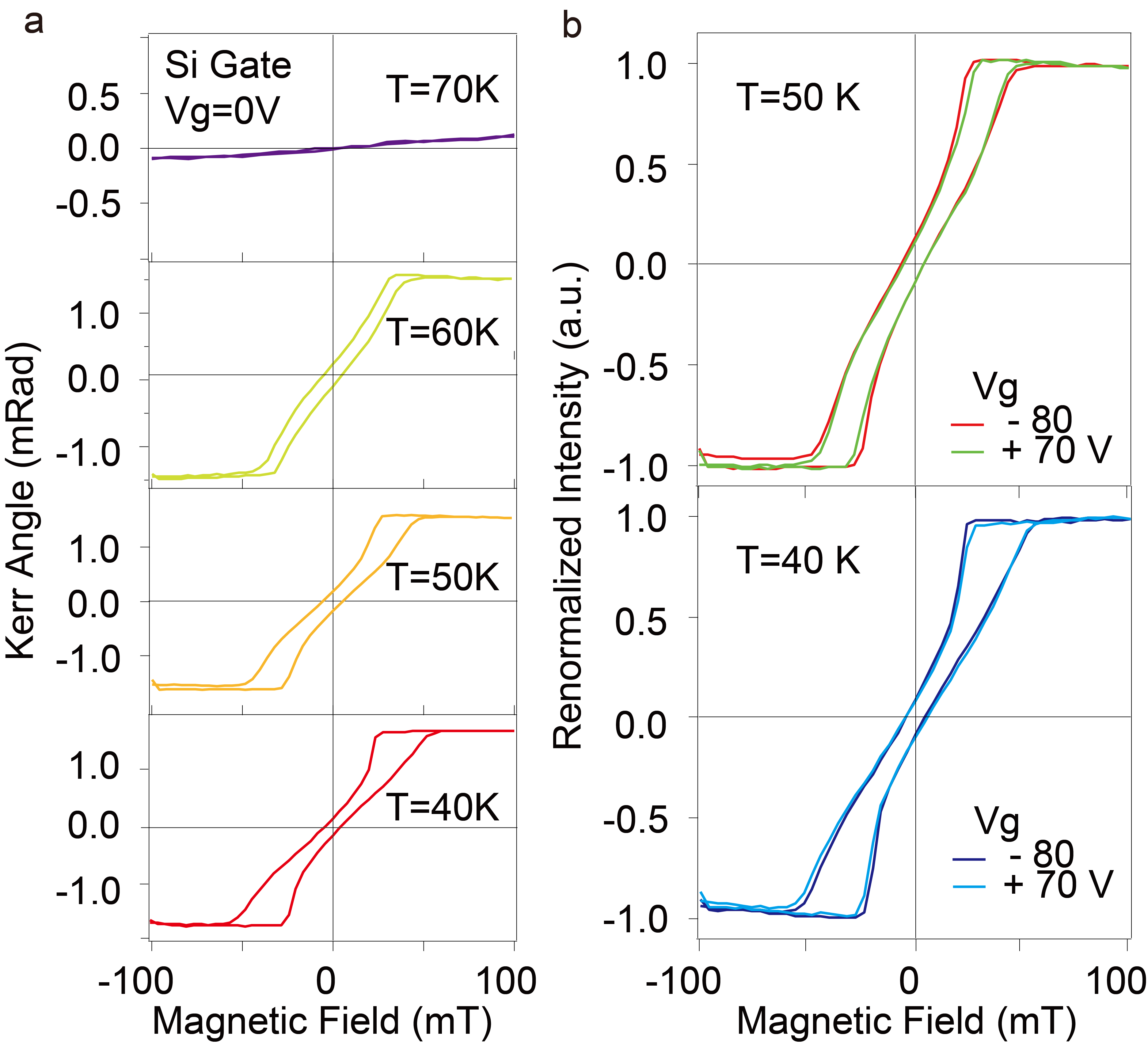
Kerr characterization of Cr2Ge2Te6 FETs with Si gate. Magneto-optic Kerr effect is known as an method to probe the magnet moment according to the changes to light reflected from a magnetized surface. It has been widely used for surface science, including the recently thrived 2D vdW magnetic materials.Morpurgo_CrI3 ; HanWei_2DMat ; XD_Xu_Nature ; Xiang_Nature Here, we use an ultra-high sensitivity Kerr setup with a low temperature vacuum cryostat to investigate the magnetization of few-layered Cr2Ge2Te6 transsitors, while monitoring their electrical transport . The optical diagram and the measuring protocols are described in the Suppl. Info. By using an objective close to sample surface, spot size of about 1 m diameter is achieved in the incident laser with a wavelength of 800 nm. Figure 2a shows a micro-area Kerr measurements at different temperatures of a Cr2Ge2Te6 device with thickness of about 19 nm. It is seen that at T=70 K, the sample behaves as paramagnetic, in good agreement with the ZFC-FC characterization of it bulk form. When decreasing temperature below 60 K, it shows ferromagnetic loops, with enhanced saturation field at lower temperature (Fig. S10).
To investigate the possible solid gate tuning of the Kerr signal, we carried out field effect measurement of the studied device, as shown in Fig. S11. A maximum gate range was determined from -80 V to +70 V, to the limit which keeps gate leakage negligible. According to the model of capacitive coupling of a Si gate with a SiO2 dielectric layer (285 nm used here), the charge carrier concentration induced per unit area, per unit Volt, is about 7.6 cm-2V-1.Yuanbo_QHE2005 Therefore, the total charge doping that took effect was at the order of 1013cm-2. However, even with the largest possible gate voltages applied in the Cr2Ge2Te6 transistors, no obvious tuning of Kerr signal was observed at TTC, as shown in Fig. 2b.
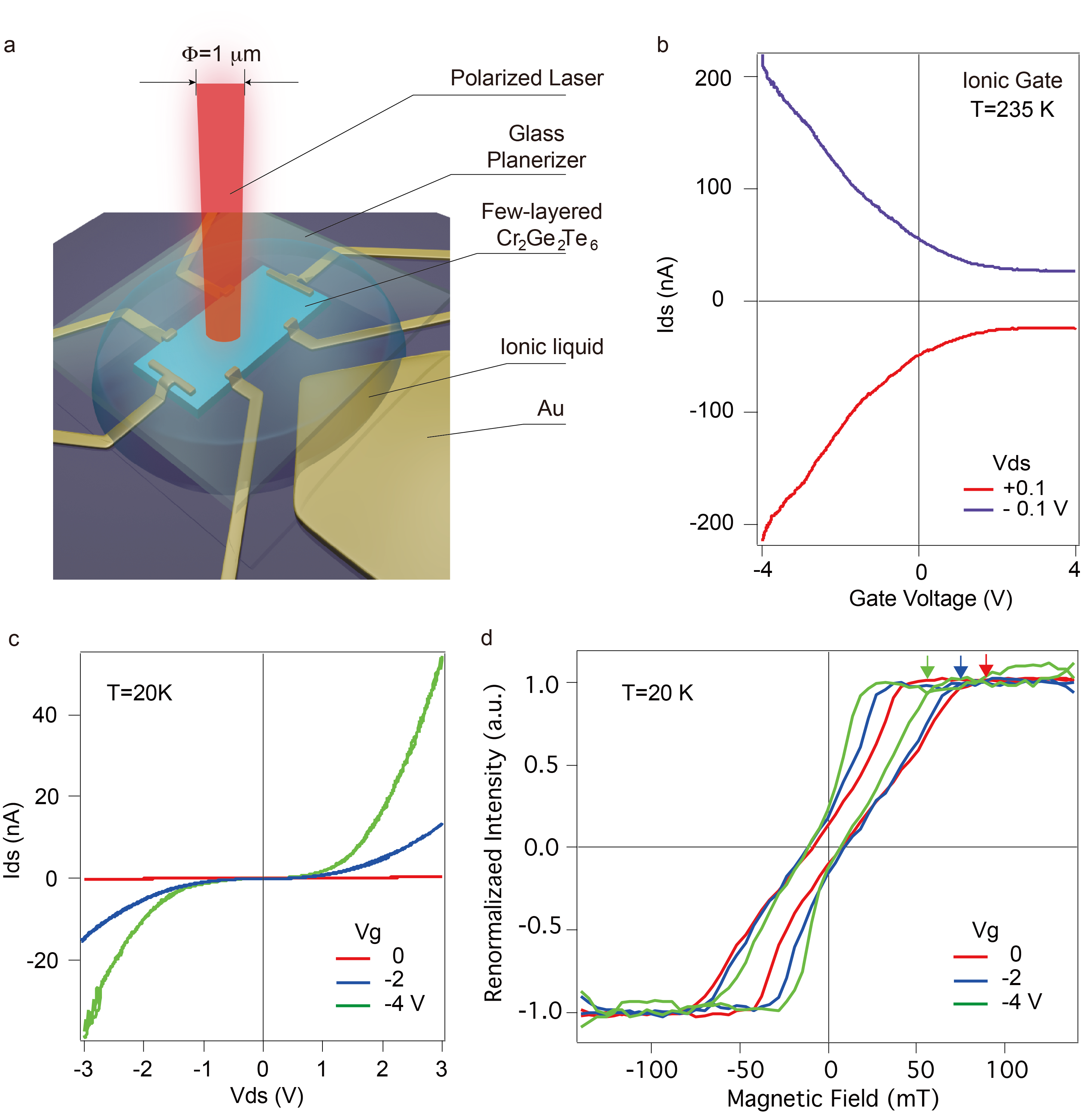
Kerr characterization of Cr2Ge2Te6 FETs with ionic gate. In the following, we discuss the measurement of Cr2Ge2Te6 FETs using an ionic liquid as gate dielectric. Ionic liquid such as are often used in gate tuning semiconductor conducting channels, because of the molecular in the liquid can form an electric double-layer (EDL) that significantly reduces the thickness as compared to conventional solid dielectric materials.Iwasa_NM2010 ; Hongtao_JACS2010 ; Morpurgo_NanoLett2015 It is therefore also referred to as EDL transistors.
Figure 3a shows a schematic image of a 20 nm thick Cr2Ge2Te6 flake on a Si/SiO2 substrate contacted by a Cr/Au (5/50 nm) electrodes. Together with the contacts, a large area pad acting as gate was defined close to the sample. To form the ionic-gated FET, a small droplet of ionic liquid DEME-TFSI was placed onto the device and the gate pad, followed by a glass cap that covers the whole area. Only this way it will then allow the incident of laser for further Kerr measurement. Before starting cooling, the device was left in vacuum at room temperature at a pressure of mbar for a few hours. It was then cooled down to 235 K (above the freezing point of DEME-TFSI Iwasa_NanoLett2012 ) first to test the field effect curves.
As shown in Fig. 3b, within a chemical window of 4 V (see more details in the Suppl. Info.), the sample is stable and a strong field effect can be obtained, with a gate tuned ratio of about 10 (defined as the ratio of between gate voltage =-4 V and +4 V). IV characteristics show linear behaviors at all gate voltages at 235 K, as shown in Fig. S13. Notice that the field effect curve is stabilized after several thermal cycles (Suppl. Info.) as there is a surface potential reconfiguration process until a stable state is reached.Morpurgo_NanoLett2015 Once the field effect curve is stabilized, we started cool down the sample below TC for Kerr measurements. Figure 3c shows IV characteristics of the same device with fixed ionic gate voltages of 0, -2 and -4V, that is measured at 20 K, respectively. A semiconducting output curve is seen at low temperature, but with a much higher compared with those obtained in the Si gated devices for similar Cr2Ge2Te6 flake thickness.
Strikingly, unlike the Si gated Cr2Ge2Te6 FETs (Fig. 2b), renormalized magnetization loop of the devices gated by ionic liquid can be largely tuned as shown in Fig. 3d. Take the -4Vg loop for example, the saturation field Hs, indicated by gray and black arrows in Fig. 3d, can be modified by a factor of 2 compared to the values of the loop measured at Vg=0V. For the ionic liquid DEME-TFSI used here, the gate induced carrier density has been widely studied before, which reaches about 1.0 and 0.75 cm-2 for electrons and holes at = 3 V, respectively, which are usually about 100 times higher per volt than that found in solid-state FETs with 285 nm oxides.Morpurgo_NanoLett2015 ; Iwasa_NanoLett2012
III Discussion
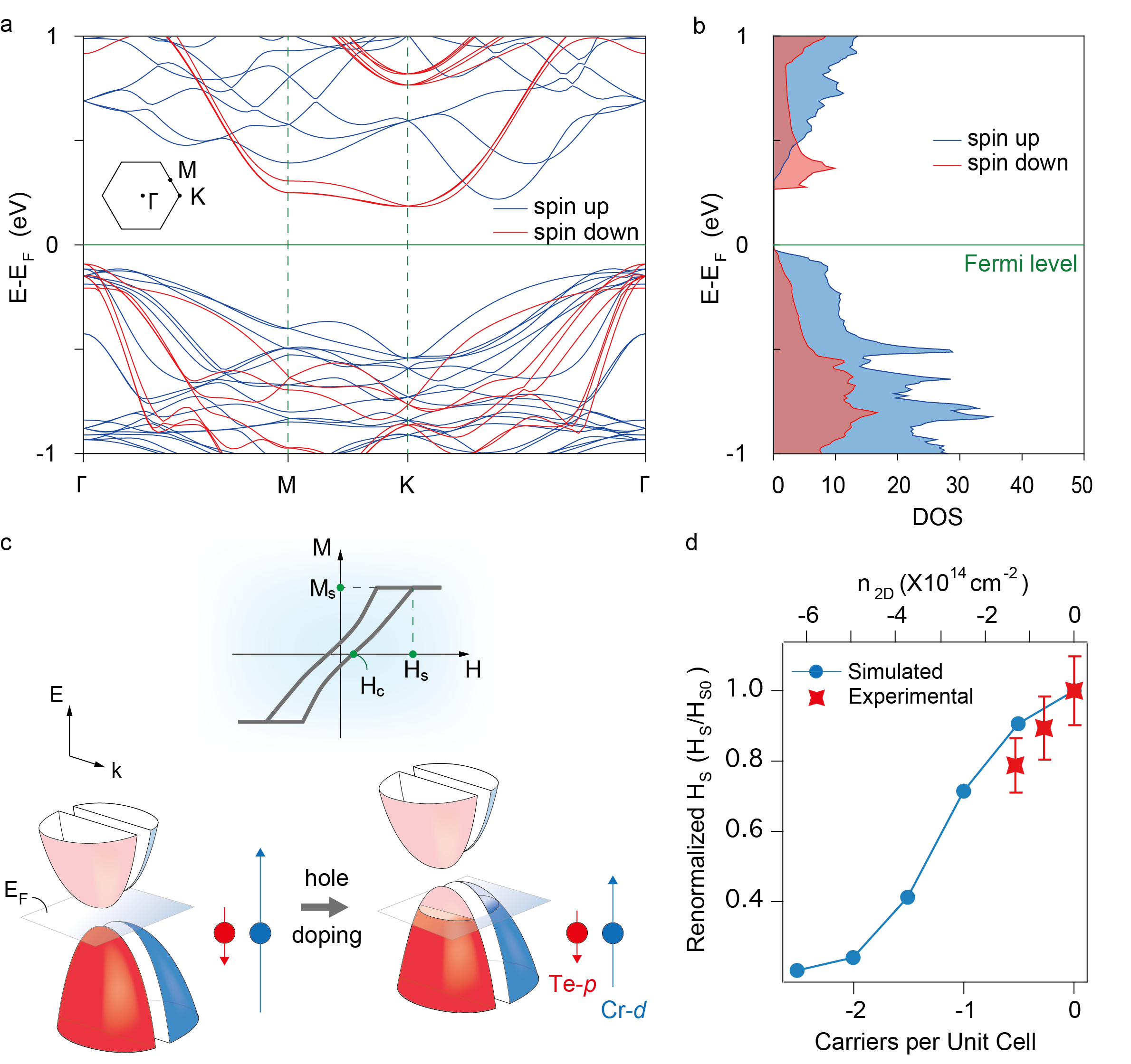
In the following, we compare the measured data with first-principles simulations. Given that our experimental Cr2Ge2Te6 flakes are more than 18 nm in their thicknesses, we here invoke a 3-layer bulk phase of Cr2Ge2Te6 for computational simplicity. The lattice parameters are drawn from the Rietveld refinement of our X-ray diffraction data and are consistent with the Springer Materials database.SMdatabase In Fig. 4a,b, we show electron band structure and density of states (DOS). Cr2Ge2Te6 is a ferromagnetic semiconductor, and its spin majority bands are mainly contributed by orbital of Cr atoms and spin minority bands from the orbital of Te atoms in both valence and conduction bands near the band gap, as seen from projected DOS in Fig.S15. Hole doping (electron doping) by electrostatic gating will shift the Fermi level into valence (conduction) band by depleting (filling) more Cr- orbitals than Te- orbitals, which leads to a reduced net magnetic moment and saturated moment under magnetic field, as indicated in the schematic picture in Fig. 4c.
In order to see how coercivity field Hc and saturation field Hs changes with electrostatic doping, we calculate the dependence of energy on both net spin moment and doping level by combining the density function theory and the fixed spin moment methodMoruzzi86 . As shown in Fig.S16, for all studied hole doping level from 0.0 to 1.5 carriers/unit cell, energy profile exhibits a bi-stable electronic ground state at mgs 0, exhibiting a typical ferromagnetism. As mentioned earlier, mgs decreases with increasing the doping level. Meanwhile, both coercivity field (Hc) and saturation field (Hs) are extracted from the calculated energy profile, namely Hc,s = (definitions of Hs and Hc are indicated in the upper panel of Fig.4c). More details will be given in the methods part.
Weisheit et al. reported that magnetocrystalline anisotropy KU of FePt and FePd 2 nm thin films can be reversibly modified by an applied electric field with the EDL technique.Weisheit_Science_2007 In their case, the measurable that changes with ionic gate doping is mainly the coercivity that differs for around 3 (compared to 50 Hs obtained in this work). They assumed the Hc to be directly proportional to the KU, and can be evaluated with respect to KU energies derived from electronic structure calculations.Weisheit_Ref9 Here, the obtained in the few-layered Cr2Ge2Te6 devices are very weak and the trend of modification is below the detection sensitivity of our set-up. We therefore will mainly focus on the electric-field modification of Hs, as well as the amplitude of Kerr angle (, the saturated magnetization, Ms) recorded at different gate doping.
In Fig. 4d, we show the carrier density dependence of the saturation field Hs (normalized by the zero-doping Hs(0)) in blue solid line. Hs goes down along with the increasing hole carrier concentration, which agrees well with the experimental data shown in red star. In contrary, the coercivity field Hc has a very weak doping level dependence, as shown in Fig. S17. Meanwhile, shown in Fig. S18, experimentally a reduced Ms is observed with increasing hole doping, which is in qualitative agreement with the simulated result in Fig. S17. The doping-induced effect can be comprehended as follows. From the schematic picture in Fig. 4c, saturation field Hs needed for reversing the minority spin is expected to go down with increased hole concentration. While the coercivity field Hs is strongly relevant to magneto-crystalline anisotropy energy (MAE). Our calculation shows that MAE between in-plane and out-of-plane magnetization direction is quite small (at least one order of magnitude smaller than soft iron.) and MAE has no obvious dependence on doping level of interest here.
In conclusion, we have demonstrated that few-layered semiconducting Cr2Ge2Te6 devices can serve as transistors that exhibit a gate-tuned modification of magnetism, which is obtained from the micro-area Kerr measurements below the ferromagnetic Curie temperature with ionic liquid gating. The observed behavior of gate-tuned magnetism in few-layered Cr2Ge2Te6 may be attributed to a re-balance of spin polarized band structure while tuning its Fermi level. Our findings therefore prove that vdW magnet can be a promising platform that may open further opportunities for future applications in spin-transistors.
IV Methods
Single crystal Cr2Ge2Te6 was prepared via the Te self-flux method. Raw material powders with stoichiometric ratio of Cr (purity 99.9): Ge (purity 99.9):Te (purity 99.99)=1:4:20 were mixed and kept at 950 oC for 6 h. The mixture was then cooled at the rate of 2 oC h-1, followed by a centrifuge at 500 oC.
As depicted in the Suppl. Info., Kerr rotation was performed to monitor the electrically tunable out-of-plane magnetization of the sample investigated. A cw Ti-Sapphire laser of 100 kHz bandwidth was used to generate linearly-polarized light and the probe energy was fixed at 1.550 eV for all measurements. By means of a lens with a numerical aperture of 0.50, the Gaussian beam was tightly focused with a sigma width of 1.5 m on the sample surface. A balanced photo diode bridge is adopted to sensitively monitor the polarization change of the probe beam due to the polar magneto-optic Kerr effect (MOKE). The sample was mounted strain-free in Faraday geometry in a helium-free cryostat, , both the external magnetic field applied and the light propagation vector are along the out-of-plane direction of the sample. The sample can be moved by an x-y-z piezo stage with an accuracy of 200 nm, and the sample temperature can be set from 4.0 K to 350 K. To characterize the coercive field and saturation magnetization of the sample, MOKE loop measurements were performed continuously by scanning longitudinal magnetic field from a negative to a positive , and backwards to -, which produced the MOKE loops recorded at various experiment conditions.
The simulations in this work are carried out by using the first-principles density functional theory as implemented in the VASP codeVASP . Projector augmented wave (PAW) pseudopotentials PAWPseudo and the Perdew-Burke-Ernzerhof (PBE) PBE functional are respectively used to describe electron-ion interaction and electronic exchange-correlation interaction. The Brillouin zone of the primitive unit cell is sampled by -points Monkhorst-Pack76 . We adopt eV as the electronic kinetic energy cutoff for the plane-wave basis and eV as the criterion for reaching self-consistency. Fixed-spin moment method Moruzzi86 is used to simulate energy-moment behavior. Saturation and coercivity fields are obtained by Hc,s = . Coercivity point are chosen at the inflex m point (maximum of ) between m = 0 and mgs and saturation point chosen at the m point where 20-p valence electrons giving rise to saturated magnetization ms, with p as the doping level. The magneto-crystalline anisotropy energy is calculated by using a more dense k mesh, i.e., -points.
V ACKNOWLEDGEMENT
This work is supported by the National Natural Science Foundation of China (NSFC) with Grant 11504385 and 51627801, and is supported by the National Key RD Program of China (2017YFA0206302). Z.D. Zhang acknowledges supports from the NSFC with grant 51331006 and the CAS under the project KJZD-EW-M05-3. T.Yang acknowledges supports from the Major Program of Aerospace Advanced Manufacturing Technology Research Foundation NSFC and CASC, China (No. U1537204). The work in Shanxi University is financially supported by the NSFC (Grant No. 61574087) and the Fund for Shanxi “1331 Project” Key Subjects Construction (1331KSC).
VI Author contributions
Z.H. and Z.-D.Z. conceived the experiment and supervised the overall project. Z.W. fabricated the samples. Z.W., T.-Y.Z., Y.-X.L., Y.-S.C., and Z.H. carried out experimental measurements; S.O. provided the ionic liquid and advised on the experiment; B.-J.D. and T.Y. conducted the theoretical simulations. The manuscript was written by Z.H., Y.-S.C., and T. Y. with discussion and inputs from all authors.
References
- (1) Novoselov, K. S. et al. A roadmap for graphene. Nature 490, 192–200 (2012).
- (2) Novoselov, K. S., Mishchenko, A., Carvalho, A. & Neto, A. H. C. 2D materials and van der waals heterostructures. Science 353, 461 (2016).
- (3) Dean, C. R. et al. Boron nitride substrates for high-quality graphene electronics. Nature Nanotechnology 5, 722 (2010).
- (4) Guimares, M. H. D. et al. Controlling spin relaxation in hexagonal bn-encapsulated graphene with a transverse electric field. Phys. Rev. Lett. 113, 086602 (2014).
- (5) Liu, Y. et al. Van der waals heterostructures and devices. Nature Rev. Mat. 1, 16042 (2016).
- (6) Ye, J. T. et al. Superconducting dome in a gate-tuned band insulator. Science 338, 1193 (2012).
- (7) Sachs, B., Wehling, T. O., Novoselov, K. S., Lichtenstein, A. I. & Katsnelson, M. I. Ferromagnetic two-dimensional crystals: Single layers of K2CuF4. Phys. Rev. B 88, 201402 (2013).
- (8) McGuire, M. A., Dixit, H., R, C. V. & Sales, B. C. Coupling of crystal structure and magnetism in the layered, ferromagnetic insulator CrI3. Chem. Mater. 27.
- (9) Tian, Y., Gray, M. J., Ji, H., Cava, R. J. & Burch, K. S. Magneto-elastic coupling in a potential ferromagnetic 2D atomic crystal. 2D Mater. 3, 025035 (2016).
- (10) Sivadas, N., Daniels, M. W., Swendsen, R. H., Okamoto, S. & Xiao, D. Magnetic ground state of semiconducting transition-metal trichalcogenide monolayers. Phys. Rev. B 91, 235425 (2015).
- (11) McGuire, M. A. Crystal and magnetic structures in layered, transition metal dihalides and trihalides. Crystals 7, 121 (2017).
- (12) Lee, S., Choi, K. Y., Lee, S., Park, B. H. & Park, J. G. Tunneling transport of mono- and fewlayers magnetic van der Waals MnPS3. Apl Mater. 4, 086108 (2016).
- (13) May, A. F., Calder, S., Cantoni, C., Cao, H. B. & McGuire, M. A. Magnetic structure and phase stability of the van der Waals bonded ferromagnet Fe3-xGeTe2. Phys. Rev. B 93, 014411 (2016).
- (14) Liu, B. J. et al. Critical behavior of the quasi-two-dimensional semiconducting ferromagnet CrSiTe3. Scientific Reports 6, 33873 (2016).
- (15) Kurumaji, T. et al. Magnetic-field induced competition of two multiferroic orders in a triangular-lattice helimagnet MnI2. Phys. Rev. Lett. 106, 167206 (2011).
- (16) Ashton, M., Paul, J., Sinnott, S. B. & Hennig, R. G. Topology-scaling identification of layered solids and stable exfoliated 2D materials. Phys. Rev. Lett. 118, ‘06101 (2017).
- (17) Mounet, N. et al. Two-dimensional materials from high-throughput computational exfoliation of experimentally known compounds. Nature Nanotechnol. doi:10.1038/s41565–017–0035–5 (2018).
- (18) Mermin, N. D. & Wagner, H. Absence of ferromagnetism or antiferromagnetism in one- or two-dimensional isotropic heisenberg models. Phys. Rev. Lett. 17, 1133–1136 (1966).
- (19) Huang, B. et al. Layer-dependent ferromagnetism in a van der waals crystal down to the monolayer limit. Nature 546, 270–273 (2017).
- (20) Gong, C. et al. Discovery of intrinsic ferromagnetism in two-dimensional van der waals crystals. Nature 546, 265–269 (2017).
- (21) Lee, J. U. et al. Ising-type magnetic ordering in atomically thin FePS3. Nano Lett. 16, 7433–7438 (2016).
- (22) Wang, X. et al. Raman spectroscopy of atomically thin two-dimensional magnetic iron phosphorus trisulfide (FePS3) crystals. 2D Mater. 3, 031009 (2016).
- (23) Williams, T. J. et al. Magnetic correlations in the quasi-two-dimensional semiconducting ferromagnet CrSiTe3. Phys. Rev. B 92, 144404 (2015).
- (24) Arai, M. et al. Construction of van der waals magnetic tunnel junction using ferromagnetic layered dichalcogenide. Appl. Phys. Lett. 107, 103107 (2015).
- (25) Li, B. et al. A two-dimensional Fe-doped SnS2 magnetic semiconductor. Nat. Commun. 8, 1958 (2017).
- (26) Radhakrishnan, S. et al. Fluorinated h-BN as a magnetic semiconductor. Science Advances 3, e1700842 (2017).
- (27) Wang, Z. et al. Very large tunneling magnetoresistance in layered magnetic semiconductor CrI3. arXiv 1801.08188 (2018).
- (28) Klein, D. R. et al. Probing magnetism in 2D van der waals crystalline insulators via electron tunneling. arXiv 1801.10075 (2018).
- (29) Song, T. C. et al. Giant tunneling magnetoresistance in spin-filter van der waals heterostructures. arXiv 1801.08679 (2018).
- (30) Lin, M. W. et al. Ultrathin nanosheets of CrSiTe3: a semiconducting two-dimensional ferromagnetic material. J. Mater. Chem. C 4, 315 (2016).
- (31) Xing, W. et al. Electric field effect in multilayer Cr2Ge2Te6 : a ferromagnetic 2d material. 2D Mater. 4, 024009 (2017).
- (32) Chappert, C., Fert, A. & Nguyen Van Dau, F. The emergence of spin electronics in data storage. Nature Mater. 6, 813–823 (2007).
- (33) Matsukura, F., Tokura, Y. & Ohno, H. Control of magnetism by electric fields. Nature Nanotechnol. 10, 209 (2015).
- (34) Cherifi, R. O. et al. Electric-field control of magnetic order above room temperature. Nature Materials 13, 345–351 (2014).
- (35) Chiba, D. et al. Electrical control of the ferromagnetic phase transition in cobalt at room temperature. Nature Materials 10, 853 (2011).
- (36) Weisheit, M. et al. Electric field-induced modification of magnetism in thin-film ferromagnets. Science 315, 349–351 (2007).
- (37) Wang, W. G., Li, M., Hageman, S. & Chien, C. L. Electric-field-assisted switching in magnetic tunnel junctions. Nature Materials 11, 64 (2012).
- (38) Maruyama, T. et al. Large voltage-induced magnetic anisotropy change in a few atomic layers of iron. Nature Nanotechnol. 4, 158 (2009).
- (39) Wang, Y. Y. et al. Electrical control of the exchange spring in antiferromagnetic metals. Adv. Mater. 27, 3196–3201 (2015).
- (40) Ohno, H. et al. Electric-field control of ferromagnetism. Nature 408, 944 (2000).
- (41) Chiba, D., Yamanouchi, M., Matsukura, F. & Ohno, H. Electrical manipulation of magnetization reversal in a ferromagnetic semiconductor. Science 301, 943 (2003).
- (42) Liu, W. L. et al. Effect of aging-induced disorder on the quantum transport properties of few-layer WTe2. 2D Mater. 4, 011011 (2017).
- (43) Zhang, Y. B., Tan, Y. W., Stormer, H. L. & Kim, P. Experimental observation of the quantum hall effect and Berry’s phase in graphene. Nature 438, 201–204 (2005).
- (44) Ye, J. T. et al. Liquid-gated interface superconductivity on an atomically flat film. Nature Materials 9, 125 (2010).
- (45) Yuan, H. T. et al. Hydrogenation-induced surface polarity recognition and proton memory behavior at protic-ionic-liquid/oxide electric-double-layer interfaces. J. Am. Chem. Soc. 132, 6672–6678 (2010).
- (46) Jo, S., Costanzo, D., Berger, H. & Morpurgo, A. F. Electrostatically induced superconductivity at the surface of WS2. Nano Letters 15, 11997–1202 (2015).
- (47) Zhang, Y. J., Ye, J. T., Matsuhashi, Y. & Iwasa, Y. Ambipolar mos2 thin flake transistors. Nano Letters 12, 1136–1140 (2012).
- (48) Springer Materials database .
- (49) Moruzzi, V. L., Marcus, P. M., Schwarz, K. & Mohn, P. Ferromagnetic phases of bcc and fcc fe, co, and ni. Phys. Rev. B 34, 1784–1791 (1986). URL https://link.aps.org/doi/10.1103/PhysRevB.34.1784.
- (50) Daalderop, G. H. O., Kelly, P. J. & Schuurmans, M. F. H. Magnetocrystalline anisotropy and orbital moments in transition-metal compounds. Phys. Rev. B 44, 12054(R) (1991).
- (51) Kresse, G. & Furthmüller, J. Efficient iterative schemes for ab initio total-energy calculations using a plane-wave basis set. Phys. Rev. B 54, 11169–11186 (1996).
- (52) Kresse, G. & Joubert, D. From ultrasoft pseudopotentials to the projector augmented-wave method. Phys. Rev. B 59, 1758–1775 (1999). URL http://link.aps.org/doi/10.1103/PhysRevB.59.1758.
- (53) Perdew, J. P., Burke, K. & Ernzerhof, M. Generalized gradient approximation made simple. Phys. Rev. Lett. 77, 3865–3868 (1996). URL http://link.aps.org/doi/10.1103/PhysRevLett.77.3865.
- (54) Monkhorst, H. J. & Pack, J. D. Special points for brillouin-zone integrations. Phys. Rev. B 13, 5188–5192 (1976).