Temperature-induced topological phase transition in HgTe quantum wells
Abstract
We report a direct observation of temperature-induced topological phase transition between trivial and topological insulator in HgTe quantum well. By using a gated Hall bar device, we measure and represent Landau levels in fan charts at different temperatures and we follow the temperature evolution of a peculiar pair of ”zero-mode” Landau levels, which split from the edge of electron-like and hole-like subbands. Their crossing at critical magnetic field is a characteristic of inverted band structure in the quantum well. By measuring the temperature dependence of , we directly extract the critical temperature , at which the bulk band-gap vanishes and the topological phase transition occurs. Above this critical temperature, the opening of a trivial gap is clearly observed.
pacs:
73.21.Fg, 73.43.Lp, 73.61.Ey, 75.30.Ds, 75.70.Tj, 76.60.-kThe first two-dimensional (2D) system, in which a topological insulator (TI) phase was predicted Bernevig et al. (2006) and then experimentally observed König et al. (2007), was HgTe/CdxHg1-xTe quantum wells (QWs) with inverted band structure. The inversion of electron-like level E1 and hole-like level H1 induces spin-polarized helical edge states König et al. (2007); Roth et al. (2009); Brüne et al. (2012). When E1 and H1 levels cross, the band structure mimics a linear dispersion of massless Dirac fermions Büttner et al. (2011) corresponding to the phase transition between normal band insulator (NI) and TI states.
The QW thickness was earlier employed as a tuning parameter of these different quantum phases of matter. The crossing of the energy bands arising when equals a critical value ( nm for =0.7 and QWs grown on CdTe buffer Büttner et al. (2011)) was measured and identified as a key signature for the topological phase transition König et al. (2007); Büttner et al. (2011). However, in addition to the QW thickness, temperature Sengupta et al. (2013); Wiedmann et al. (2015) and hydrostatic pressure Krishtopenko et al. (2016a) also induces the transition between NI and TI phases across the critical gapless state. The temperature effect on the band ordering in HgTe/CdHgTe QWs is mainly caused by a strong temperature dependence of the energy gap at the point of the Brillouin zone between the and bands in HgCdTe crystals Teppe et al. (2016).
Under magnetic field, a significant way of discriminating the TI phase associated with the helical edge states of the Quantum Spin Hall Effect (QSHE), and the NI phase presenting the chiral edge states of the ordinary Quantum Hall Effect (QHE), is to probe the behavior a particular pair of Landau levels (LLs), called zero-mode LLs König et al. (2007). These zero-mode LLs split with magnetic field from the E1 and H1 subbands and correspond to the lowest LL of the conduction band and the highest LL of the valence band. In the TI phase, these E1 and H1 subbands are inverted and intersect at the sample boundaries to create the helical edge channels of the QSHE. In this case, the corresponding zero-mode LLs cross at a critical magnetic field , above which the inverted band ordering is transformed into the normal one König et al. (2007).
In the NI phase, in which E1 subband lies above H1 subband, the zero-mode LLs never cross. This can be conditionally interpreted as negative values for . Thus, corresponds to a topological phase transition between NI and TI phases. As it is for the band ordering, a critical magnetic field also depends on temperature and pressure, and therefore, can be varied by tuning these external parameters Krishtopenko et al. (2016a).
Recently, Wiedmann et al. Wiedmann et al. (2015), by analyzing magnetotransport data at high and low temperatures, have experimentally shown that the TI phase is destroyed at high temperature. However, due to high values of the critical temperature (more than 200 K) corresponding to the topological phase transition, the presence of critical gapless state was not directly observed. Another work Marcinkiewicz et al. (2017) has reported a temperature evolution of the band-gap observed by far-infrared LL spectroscopy. Although the critical temperature was found to be 90 K, an inadequate position of the Fermi level, combined with the inability to vary the carrier density in the samples, hindered a clear observation of the topological phase transition.
In this work, we report on the first clear observation of topological phase transition induced by temperature. Accurate values of and a temperature phase diagram have been extracted from LL fan charts based on magnetotransport measurements, as firstly performed by Büttner et al. Büttner et al. (2011) for different QW widths at 4.2 K. By following temperature dependence of , we define a critical temperature , at which the gapless state arises. To describe our experimental results, realistic band structure calculations, based on the eight-band Kane Hamiltonian with temperature-dependent parameters Krishtopenko et al. (2016a), have been performed.
The QW studied in this work was grown by molecular beam epitaxy (MBE) on a [013]-oriented semi-insulating GaAs substrate with a relaxed CdTe buffer Dvoretsky et al. (2010). The HgTe QW of 6.5 nm width was embedded in 40-nm Cd0.65Hg0.35Te barriers (critical thickness nm, see also Fig. 4). A 40-nm CdTe cap layer was deposited on top of the structures. The barriers from both sides of the QW were selectively doped with indium resulting in a 2D electron concentration of a few cm-2 at low temperatures. After MBE growth, 100 nm SiO2 and 200 nm Si3N4 dielectric layers were deposited on top of the structure by a plasmochemical method. The gated Hall bar has a total length of 650 m and a total width of 50 m. Magnetotransport measurements have been performed in a variable temperature insert with a base temperature K equipped with a superconducting coil. All the measurements have been done with a current of 1 nA, to avoid heating.
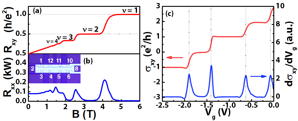
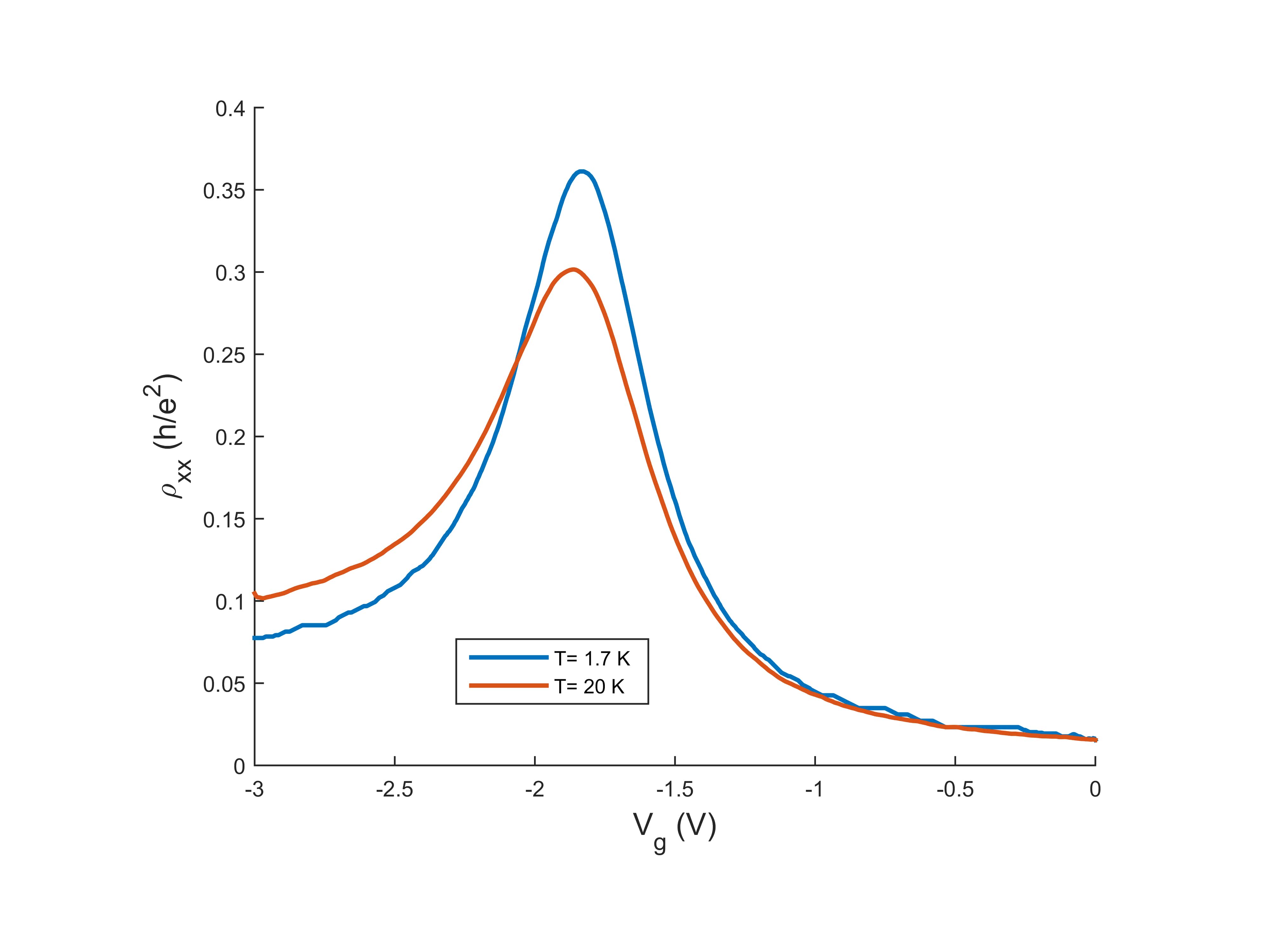
Figure 1(a,b) presents Hall resistance and Shubnikov-de Haas (SdH) oscillations at 1.7 K. The Hall resistance shows pronounced plateaus at both even and odd multiples of . The Hall conductivity as a function of the gate voltage at 1.7 K and magnetic field of 2.4 T, as well as its derivative , are both shown in the panel (c). Each peak corresponds to the crossings of the Fermi level with the given LL. This method allows for a visualization of LLs from E1 and H1 subbands and clear reconstruction of their behaviour in magnetic field.
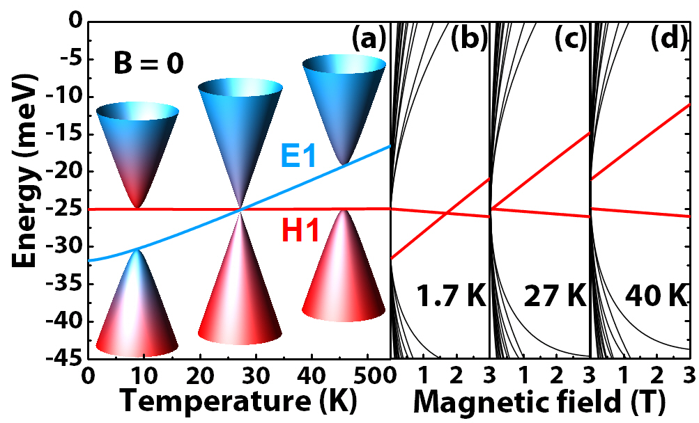
Figure 2(a) provides a temperature evolution of E1 and H1 subbands at zero quasimomentum and Fig. 2(b-d) show the corresponding LL fan charts at three different temperatures, evidencing the position of the zero mode LLs. The upper zero-mode LL level split from the conduction band has a pure heavy-hole character and its energy decreases with . By contrast, the second zero-mode LL starting from valence band has an electron component König et al. (2007) and its energy increases with .
At K, the 1 subband is well below the 1 subband and the two corresponding zero-mode LLs cross at a positive magnetic field value T. This positive characterizes the TI phase. By increasing the temperature, the width of the TI gap decreases, yielding that decreases. At a critical temperature K, the zero-mode LLs intersect at T, which means that the subbands and have the same energy and therefore the topological gap closes. At , the system hosts single-valley massless Dirac fermions Büttner et al. (2011). Above , the crossing of the zero-mode LLs can be extrapolated to a negative value of magnetic field.
To demonstrate experimentally a temperature driven phase transition in our samples, we reconstruct the LL fan chart by means of magnetotransport, measured in a wide range of gate voltages at temperatures from 1.7 K up to 40 K. As mentioned above, the derivative of the Hall conductivity has it maximum values when the Fermi level crosses one of the LLs. Therefore, plotting for each magnetic field values makes possible to visualize LL fan chart Büttner et al. (2011). This allows for accurate extraction of the critical magnetic field , at which the zero-mode LLs cross. Since is related to the changing of band ordering, the measurement of LL fan charts performed by tuning the temperature is an efficient tool to probe a temperature-induced phase transition between NI and TI phases.
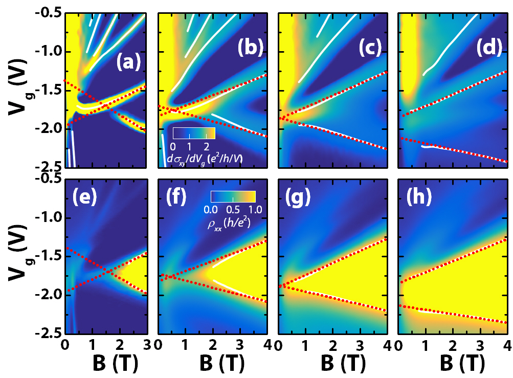
The colormaps in Fig. 3(a-d) were obtained by plotting the derivative as a function of , at different temperatures. The two zero modes LLs are observed separately above T. They seem to emerge from the resistance maximum at V, T. The trace of the zero-mode LL, originating from the H1 subband, obviously broadens and fades out at large , probably due to strong temperature dependence of mobility caused by large effective mass of holes. It becomes hardly distinguishable above 20 K. However, the zero mode LLs also coincide with and (from the semicircle relation ) Shahar et al. (1997a)).
In Fig. 3(a-d), the white curves correspond to , where is an integer. They are clearly defined up to 40 K and underline the LL positions, in agreement with the maxima. The estimated position of the two zero mode LLs do not follow the lines of constant filling factor, which implies that LLs overlap. Numerical simulations SM , performed by taking into account a LL broadening meV evidence that can be estimated from the linear extrapolation of the LL position in the NI gap, toward lower magnetic fields. The linear interpolations of the two curves for T are marked by the red dotted lines. At K, these lines cross at a finite magnetic field and give an estimate T. As increases, the crossing goes to lower magnetic fields and it finally vanishes at K. The crossing of the zero-mode LLs at zero magnetic field gives a direct indication of a critical gapless state Büttner et al. (2011), revealing a topological phase transition at K. At higher temperatures ( K, see Fig. 3(d)), the crossing of the zero-mode LLs can be extrapolated to a negative value of magnetic field, evidencing a NI phase with trivial band ordering.
To check the last point, we also plot the longitudinal resistivity in color-coded graphs as a function of and at temperatures up to 40 K, see the bottom panels in Fig. 3. The whole set of LLs is not seen here as in the top panels, but the traces of both zero-mode LLs are clearly visible at the edges of the main peak. The red dotted lines correspond to the linear fitting of the isolines of in the field range of 2.2–6 T. The crossing of the fitting lines in lower fields gives another estimate of .
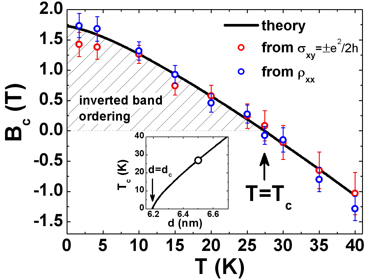
Figure 4 provides a comparison of experimental and theoretical values of critical magnetic field. Details of theoretical calculations can be found elsewhere Krishtopenko et al. (2016a). Additional analysis based on a simplified Dirac-like Hamiltonian shows that temperature evolution of is caused by temperature dependence of the band gap in our sample (see Fig. 2), while temperature effect on the dispersion of the zero-mode LLs is negligibly small SM . Two sets of experimental values have been obtained from analysis of experimental data presented in the top and bottom panels of Fig. 3. For each set, the experimental precision for is the (1) standard deviation given by the and estimates. It is seen that experimental values of from different sets reproduce quantitatively the same temperature dependence of critical magnetic field and are in good agreement with the theoretical values at all the temperatures. The critical magnetic field vanishes at K that corresponds to the formation of gapless states, in which the system mimics massless Dirac fermions Büttner et al. (2011). We formally extend our comparison toward negative values of , which correspond to the formation of the NI state. Note that the error in the determination of from increases with temperature due to broadening of the trace of the zero-mode LL, originating from the H1 subband as it is discussed above. Thus, our results shown in Fig. 4 are eloquent proof of the temperature-induced topological transition in HgTe QWs.
We note that the size of Hall bar in our sample largely exceeds the typical spin relaxation length ( m) Grabecki et al. (2013). Additional four probes resistance measurements (see section E in SM ) evidence that although the edge states exist at Tkachov and Hankiewicz (2010); Chen et al. (2012), they do not contribute significantly to the conductivity of our sample.
Finally, we discuss the role of spin-orbital corrections resulting from bulk inversion asymmetry (BIA) König et al. (2008) of zinc-blend crystals and interface inversion asymmetry (IIA) Durnev and Tarasenko (2016) on the behaviour of zero-mode LLs. Both reasons induce the anticrossing of zero-mode LLs in the vicinity of . So far, fingerprint of such anticrossing was observed only by far-infrared LL spectroscopy Marcinkiewicz et al. (2017); Orlita et al. (2011); Zholudev et al. (2012, 2015) focused on LL transitions involving the zero-mode LLs.
We note that spin-orbital corrections resulting from structure inversion asymmetry (SIA) of the QW profile does not lead to anticrossing behaviour of zero-mode LLs. Moreover, since we do not observe any beatings of SdH oscillations induced by SIA at the gate voltages presented in Fig. 3, we conclude that SIA-induced corrections are small in our sample. The latter is also confirmed by good agreement between our experimental data and calculations performed for the symmetrical QW profile.
The linear dependence of energies of the zero-mode LLs and their experimental traces on magnetic field far from enables us to recalculate the anticrossing gap measured in magnetooptics Orlita et al. (2011); Zholudev et al. (2012, 2015) into the values of gate voltage, expected in our sample. For instance, by using theoretical band-gap of 7 meV at 1.7 K and T (see Fig. 2) and its experimental value V represented in the scale of (see Fig 3(e)), we find that the experimental values of 4-5 meV transform into 0.4–0.5 V, which should be observed for our sample. As it is seen from Fig. 3, the width of experimental traces of zero-mode LLs in the vicinity of , which may be interpreted as a manifestation of the LL anticrossing, is significantly lower than the mentioned values. The latter is also consistent with previous magnetotransport results König et al. (2007); Büttner et al. (2011).
As discussed in Kadykov et al. (2016), a possible explanation of the large anticrossing gap in the vicinity of measured by far-infrared LL spectroscopy can be based on electron-electron interaction effect. The latter may largely influence close energies of LL transitions MacDonald and Kallin (1989); Bychkov and Martinez (2005); Krishtopenko et al. (2015) as we deal with strongly non-parabolic 2D system for which Kohn’s theorem Kohn (1961) does not hold.
On the other hand, both BIA and IIA induces a spin splitting of both electron-like and hole-like states at non-zero in the symmetrical QWs. If the spin splitting is strong enough, it results in the beatings arising in SdH oscillations. However, these beatings have never been observed in symmetrical HgTe QWs at low electron concentration. This is also consistent with the small strength of BIA and IIA terms, evaluated for our sample.
Finally, the presence of BIA and IIA terms induces the optical transitions between two branches of helical edge states Durnev and Tarasenko . If both terms are small only spin-dependent transitions between edge and bulk states are allowed Kaladzhyan et al. (2015). Very recent accurate measurements of a circular photogalvanic current in HgTe QWs Dantscher et al. (2017) have revealed the optical transitions between the edge and bulk states only. The latter also indicates the small effects of BIA and IIA terms in HgTe QWs.
In conclusion, we have directly observed a temperature-induced topological transition between NI and TI phases. By plotting experimental LL fan charts at different temperatures, we have accurately extracted values of critical magnetic field at different temperatures. Following experimental phase diagram, we have determined a critical temperature K, at which vanishes. Our experimental results are in good agreement with realistic band structure and LLs calculations based on the eight-band Kane Hamiltonian with temperature dependent parameters.
Acknowledgements.
The authors gratefully thanks Z. D. Kvon from the Institute of Semiconductor Physics (Siberian Branch, Russian Academy of Sciences) for processing of the samples. Part of this work was supported by the Languedoc-Roussillon region via the ”Gepeto Terahertz platform”, by Era.Net-Rus Plus project ”Terasens”, by the CNRS through ”Emergence project 2016” and LIA ”TeraMIR”, by MIPS department of Montpellier University through the ”Occitanie Terahertz Platform” and the ARPE project ”Terasens”, by and by the French Agence Nationale pour la Recherche (Grant No. ANR-16-CE09-0016 and Dirac3D project). Theoretical calculations were performed in the framework of project 16-12-10317 provided by the Russian Science Foundation. The growth of the samples were supported by the Russian Foundation for Basic Research (grants 15-52-16017, 18-52-16008). S. S. Krishtopenko and A. M. Kadykov acknowledge the Russian Ministry of Education and Science (MK-1136.2017.2 and SP-5051.2018.5).
References
- Bernevig et al. (2006) B. A. Bernevig, T. L. Hughes, and S.-C. Zhang, Science 314, 1757 (2006).
- König et al. (2007) M. König, S. Wiedmann, C. Brüne, A. Roth, H. Buhmann, L. W. Molenkamp, X.-L. Qi, and S.-C. Zhang, Science 318, 766 (2007).
- Roth et al. (2009) A. Roth, C. Brüne, H. Buhmann, L. W. Molenkamp, J. Maciejko, X.-L. Qi, and S.-C. Zhang, Science 325, 294 (2009).
- Brüne et al. (2012) C. Brüne, A. Roth, H. Buhmann, E. Hankiewicz, L. Molenkamp, J. Maciejko, Q. X.-L., and S.-C. Zhang, Nat. Phys. 8, 485 (2012).
- Büttner et al. (2011) B. Büttner, C. Liu, G. Tkachov, E. Novik, C. Brüne, H. Buhmann, E. Hankiewicz, P. Recher, B. Trauzettel, S. Zhang, and L. Molenkamp, Nat. Phys. 7, 418 (2011).
- Sengupta et al. (2013) P. Sengupta, T. Kubis, Y. Tan, M. Povolotskyi, and G. Klimeck, J. Appl. Phys. 114, 043702 (2013).
- Wiedmann et al. (2015) S. Wiedmann, A. Jost, C. Thienel, C. Brüne, P. Leubner, H. Buhmann, L. W. Molenkamp, J. C. Maan, and U. Zeitler, Phys. Rev. B 91, 205311 (2015).
- Krishtopenko et al. (2016a) S. S. Krishtopenko, I. Yahniuk, D. B. But, V. I. Gavrilenko, W. Knap, and F. Teppe, Phys. Rev. B 94, 245402 (2016a).
- Teppe et al. (2016) F. Teppe, M. Marcinkiewicz, S. S. Krishtopenko, S. Ruffenach, C. Consejo, A. M. Kadykov, W. Desrat, D. But, W. Knap, J. Ludwig, S. Moon, D. Smirnov, M. Orlita, Z. Jiang, S. V. Morozov, V. Gavrilenko, N. N. Mikhailov, and S. A. Dvoretskii, Nat. Commun. 7, 12576 (2016).
- Marcinkiewicz et al. (2017) M. Marcinkiewicz, S. Ruffenach, S. S. Krishtopenko, A. M. Kadykov, C. Consejo, D. B. But, W. Desrat, W. Knap, J. Torres, A. V. Ikonnikov, K. E. Spirin, S. V. Morozov, V. I. Gavrilenko, N. N. Mikhailov, S. A. Dvoretskii, and F. Teppe, Phys. Rev. B 96, 035405 (2017).
- Dvoretsky et al. (2010) S. Dvoretsky, N. Mikhailov, Y. Sidorov, V. Shvets, S. Danilov, B. Wittman, and S. Ganichev, J. Electron. Mater. 39, 918 (2010).
- Shahar et al. (1997a) D. Shahar, D. C. Tsui, M. Shayegan, E. Shimshoni, and S. L. Sondhi, Phys. Rev. Lett. 79, 479 (1997a).
- (13) See Supplemental Materials, which also contain Refs. [30-35], for a brief discussion of joint effects of disorder and geometric capacitance of the gated Hall bar on experimental Landau level fan charts. Analysis of temperature dependence of critical magnetic field is also provided therein .
- Grabecki et al. (2013) G. Grabecki, J. Wróbel, M. Czapkiewicz, L. Cywiński, S. Gierałtowska, E. Guziewicz, M. Zholudev, V. Gavrilenko, N. N. Mikhailov, S. A. Dvoretski, F. Teppe, W. Knap, and T. Dietl, Phys. Rev. B 88, 165309 (2013).
- Tkachov and Hankiewicz (2010) G. Tkachov and E. M. Hankiewicz, Phys. Rev. Lett. 104, 166803 (2010).
- Chen et al. (2012) J.-C. Chen, J. Wang, and Q.-f. Sun, Phys. Rev. B 85, 125401 (2012).
- König et al. (2008) M. König, H. Buhmann, L. W. Molenkamp, T. Hughes, C.-X. Liu, X.-L. Qi, and S.-C. Zhang, J. Phys. Soc. Jpn. 77, 031007 (2008).
- Durnev and Tarasenko (2016) M. V. Durnev and S. A. Tarasenko, Phys. Rev. B 93, 075434 (2016).
- Orlita et al. (2011) M. Orlita, K. Masztalerz, C. Faugeras, M. Potemski, E. G. Novik, C. Brüne, H. Buhmann, and L. W. Molenkamp, Phys. Rev. B 83, 115307 (2011).
- Zholudev et al. (2012) M. Zholudev, F. Teppe, M. Orlita, C. Consejo, J. Torres, N. Dyakonova, M. Czapkiewicz, J. Wróbel, G. Grabecki, N. Mikhailov, S. Dvoretskii, A. Ikonnikov, K. Spirin, V. Aleshkin, V. Gavrilenko, and W. Knap, Phys. Rev. B 86, 205420 (2012).
- Zholudev et al. (2015) M. S. Zholudev, F. Teppe, S. V. Morozov, M. Orlita, C. Consejo, S. Ruffenach, W. Knap, V. I. Gavrilenko, S. A. Dvoretskii, and N. N. Mikhailov, JETP Lett. 100, 790 (2015).
- Kadykov et al. (2016) A. M. Kadykov, J. Torres, S. S. Krishtopenko, C. Consejo, S. Ruffenach, M. Marcinkiewicz, D. But, W. Knap, S. V. Morozov, V. I. Gavrilenko, N. N. Mikhailov, S. A. Dvoretsky, and F. Teppe, Appl. Phys. Lett. 108, 262102 (2016).
- MacDonald and Kallin (1989) A. H. MacDonald and C. Kallin, Phys. Rev. B 40, 5795 (1989).
- Bychkov and Martinez (2005) Y. A. Bychkov and G. Martinez, Phys. Rev. B 72, 195328 (2005).
- Krishtopenko et al. (2015) S. S. Krishtopenko, A. V. Ikonnikov, M. Orlita, Y. G. Sadofyev, M. Goiran, F. Teppe, W. Knap, and V. I. Gavrilenko, J. Appl. Phys. 117, 112813 (2015).
- Kohn (1961) W. Kohn, Phys. Rev. 123, 1242 (1961).
- (27) M. V. Durnev and S. A. Tarasenko, (to be published) .
- Kaladzhyan et al. (2015) V. Kaladzhyan, P. P. Aseev, and S. N. Artemenko, Phys. Rev. B 92, 155424 (2015).
- Dantscher et al. (2017) K.-M. Dantscher, D. A. Kozlov, M. T. Scherr, S. Gebert, J. Bärenfänger, M. V. Durnev, S. A. Tarasenko, V. V. Bel’kov, N. N. Mikhailov, S. A. Dvoretsky, Z. D. Kvon, J. Ziegler, D. Weiss, and S. D. Ganichev, Phys. Rev. B 95, 201103 (2017).
- Dykhne and Ruzin (1994) A. M. Dykhne and I. M. Ruzin, Phys. Rev. B 50, 2369 (1994).
- Polyakov and Shklovskii (1993) D. G. Polyakov and B. I. Shklovskii, Phys. Rev. Lett. 70, 3796 (1993).
- Bennaceur et al. (2012) K. Bennaceur, P. Jacques, F. Portier, P. Roche, and D. C. Glattli, Phys. Rev. B 86, 085433 (2012).
- Abrikosov (1998) A. A. Abrikosov, Physical Review B 58, 2788 (1998).
- Krishtopenko et al. (2016b) S. S. Krishtopenko, W. Knap, and F. Teppe, Sci. Rep. 6, 30755 (2016b).
- Shahar et al. (1997b) D. Shahar, D. Tsui, M. Shayegan, E. Shimshoni, and S. Sondhi, Phys. Rev. Lett. 79, 479 (1997b).
Supplemental Materials
.1 A. Hall carrier density vs gate voltage
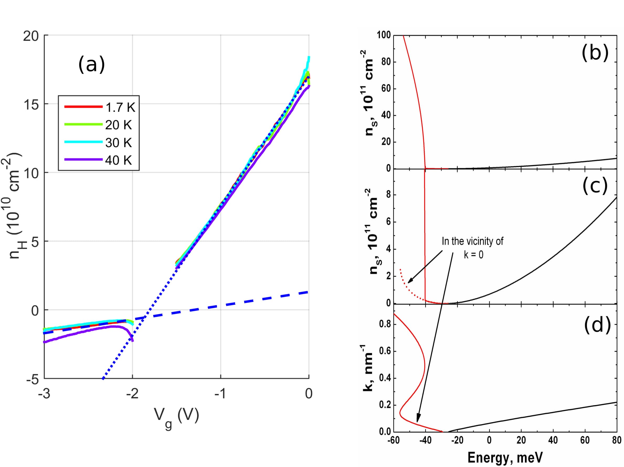
The Hall carrier density was first determined at various temperatures as a function of the gate voltage . No significant difference in the carrier density was found along the Hall bar. Fig. S1a shows estimated from the Hall resistance . The geometric capacitance is theoretically equal to cmeV. It is in good agreement with the observed slope cm-2/V on the electron side.
By contrast, the experimental slope is significantly lower than expected on the hole side, for V. The hole density remains pinned close to 1–2 cm-2. This experimental observation is in good agreement with the band structure calculation. Figure. S1(b-d) shows that on the hole side, 10 meV below the topological band gap, a valence band side maximum is present which can accumulate more than cm-2 holes. By contrast, holes with a small momentum are also present, but with a much smaller density. These holes have a higher velocity and are expected to be much more mobile. The holes trapped in the side maximum have a too small mobility to be detected in the Hall coefficient, which is given only by the contribution of the holes close to . However, the overall large hole density reduces significantly the gate efficiency and pins the Fermi level approximately 10 meV below the band gap.
.2 B. Interpreting data at higher magnetic field
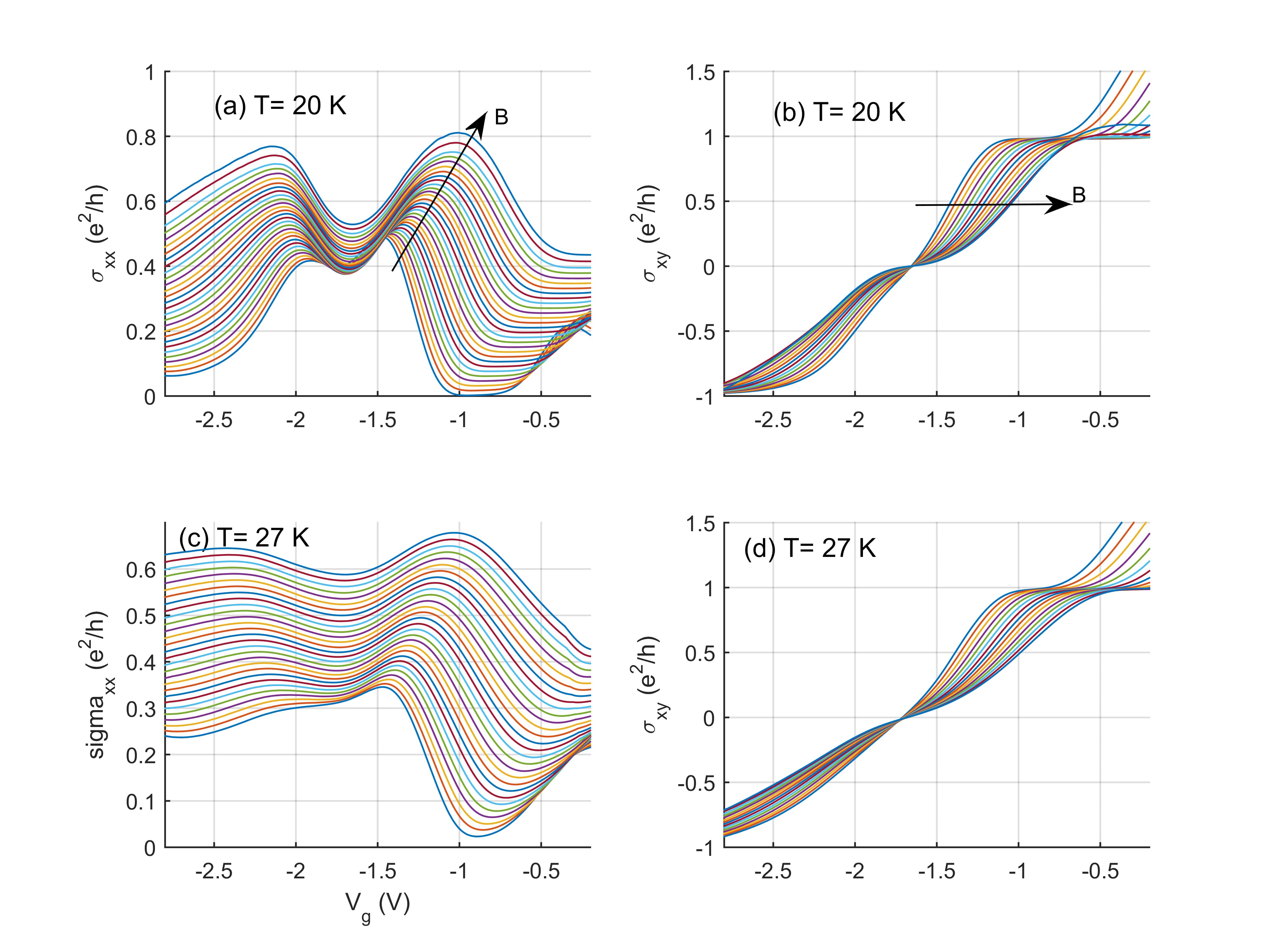
Figure S2 shows the evolution of the conductivities at large magnetic fields, 3.2 – 6 T for two temperatures. Two maxima are clearly distinguishable in the longitudinal conductitivities. When the temperature increases, the voltage difference between the two maxima also increases. This is the key signature of the progressive transformation of the TI gap into a NI gap. Simultaneously, the gate voltage between the two conductivities corresponding to also increases with and , see panels (b) and (d).
Figure 3(e,f) (main text) shows colormaps of the longitudinal magnetoresistance measured at K and K. At T, a resistance maximum is identified around V, which corresponds to the topological gap. In increasing magnetic field, Landau levels are clearly distinguishable on the electron side ( V). On the hole side ( V), LLs are also observed, with a very small dependence on . The carrier density extracted from the periodicity of these LLs is in agreement with the Hall density obtained at low field. Following the above arguments, the LLs observed for V are associated to holes close to , whereas the LLs associated to the hole side maximum of the valence band are not observed.
Remarkably, the resistance shows a clear saddle point around T and V. This saddle point originates from the crossing of the two zero-modes LLs and its observation is possible because of the presence of disorder. To show this, let us assume that the LLs have a Lorentzian broadening . Because the energy difference between adjacent LLs is comparable to , the LLs overlap. At the maximum of the density of states of the LL of index , the filling factor does not correspond to an half-integer. It is given by:
| (1) |
which can be simplified as:
| (2) |
where is the LL index and is the energy of the LL as calculated theoretically. The sign refers to LLs associated either to the conduction or the valence bands respectively. The only fitting parameter is the LL broadening .
The filling factor is directly related to the gate voltage by the geometric capacitance: , where is a constant. The quantum capacitance is negligible in our geometry. From the above equations, the positions of the LLs can be calculated as a function of and . The calculated position of the first LLs of the conduction band are shown in Fig. S3(e-h) in the ) plane as dashed white lines, superposed to , and in Fig. S3(a-d) superposed to the derivative of the experimental transverse conductivity . To obtain a good agreement with data, we have chosen meV.
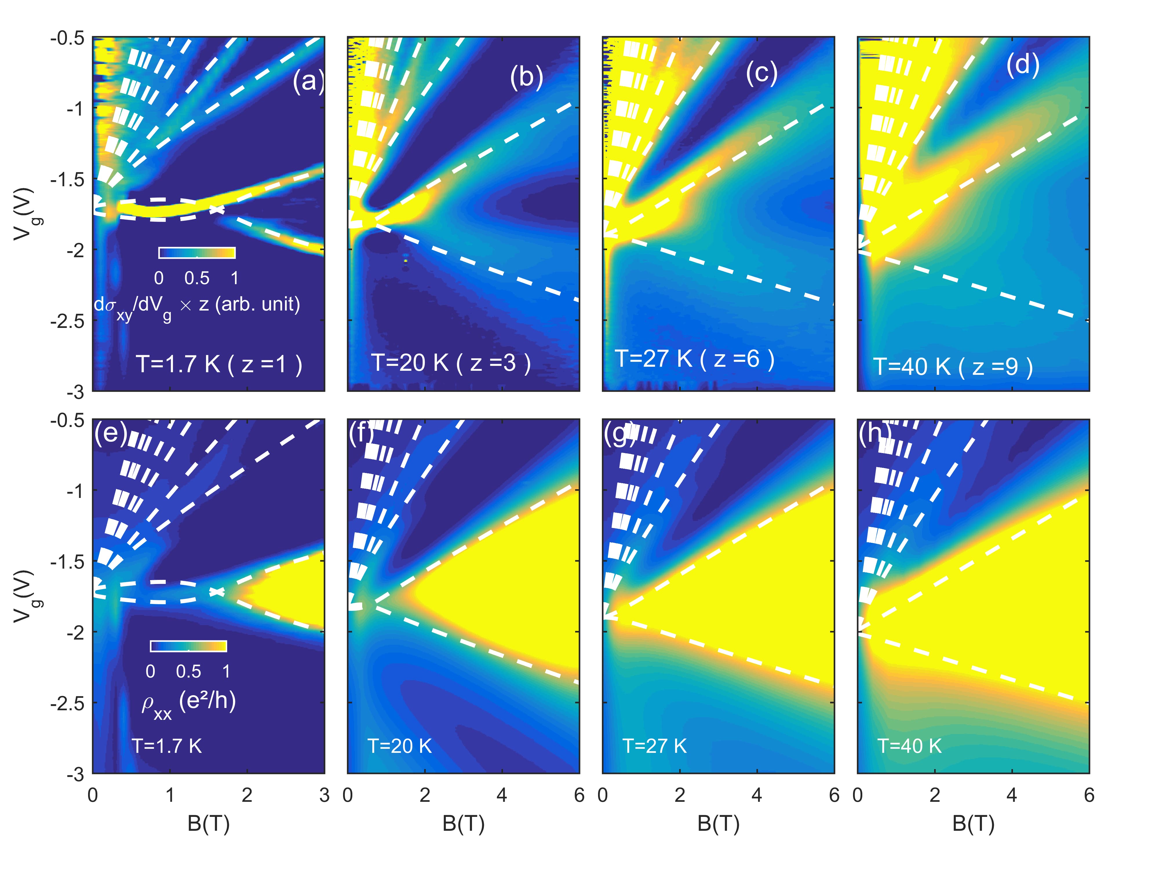
Most of the LLs follow straight lines, as expected if the LL overlap is negligible: the LL position is then given by a constant close to a half-integer. However, the evolution of the two zero mode LLs is much more complex, because these LLs cross at the critical field where . Let us stress that the two zero mode LLs emerge from the and bands, respectively, which are separated by an energy gap of several meV. Nevertheless, from Fig. S3, these two LLs seem to emerge from the same gate voltage at T. The reason for this is that the gate voltage is proportional to the net carrier density. As our model does not include any disorder in the topological gap at T, the two LLs merge at T in the plane.
.3 C. Estimation of
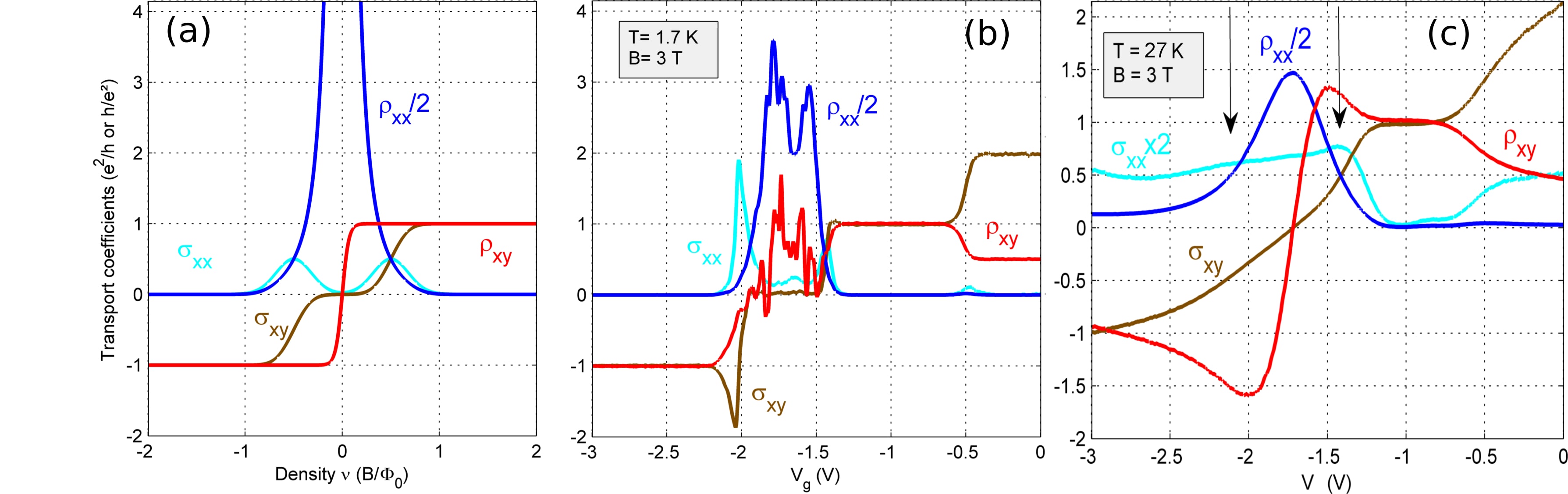
To get an estimate of , the position of the two zero mode LLs must be determined accurately from the data. Fig. S4a sketches the theoretical evolution of both conductivity and resistivity when the filling factor is varied across the normal gap, at high . The LLs at correspond to i) a maximum of the longitudinal conductivity ; ii) a value of the transverse conductivity; iii) a maximum of the derivative ; iv) a value for the longitudinal resistivity , as far as the semicircle relation remains valid Dykhne and Ruzin (1994); Shahar et al. (1997).
Fig. S4b and S4c show the experimental transport coefficients at T, K and K, respectively. The relations (i)-(iv) are indeed satisfied. however, at the highest temperature, the maxima of (indicated by arrows) and almost disappeared, whereas and are still quite close to their expected values. Therefore the conditions ii) and iv) have been used preferentially to find the position of the LLs at magnetic fields above 2.2 T for different temperatures. We have chosen T as a minimal threshold because this is the lowest magnetic field for which we still observe when (with an uncertainty of 3% ).
A linear extrapolation of these isolines and toward low magnetic field gives two estimates of . For each estimate, a mean value and a standard deviation () can be calculated by varying the magnetic field interval on which the linear fit is done.
.4 D. Conductivity mechanisms in the NI gap
Figure S5 shows the maximum of the magnetoresistance around () from T to T, at two temperatures. At K, the resistance dip is rather large (from T to 1.5 T) with a minimum around T. The resistance falls below the expected theoretical value of , possibly because of additional parallel conduction. At higher temperature K, the resistance dip is better defined and appears at T. As the minimum goes to higher when increases, its position cannot be directly related to the crossing of the two zero-mode LLs.
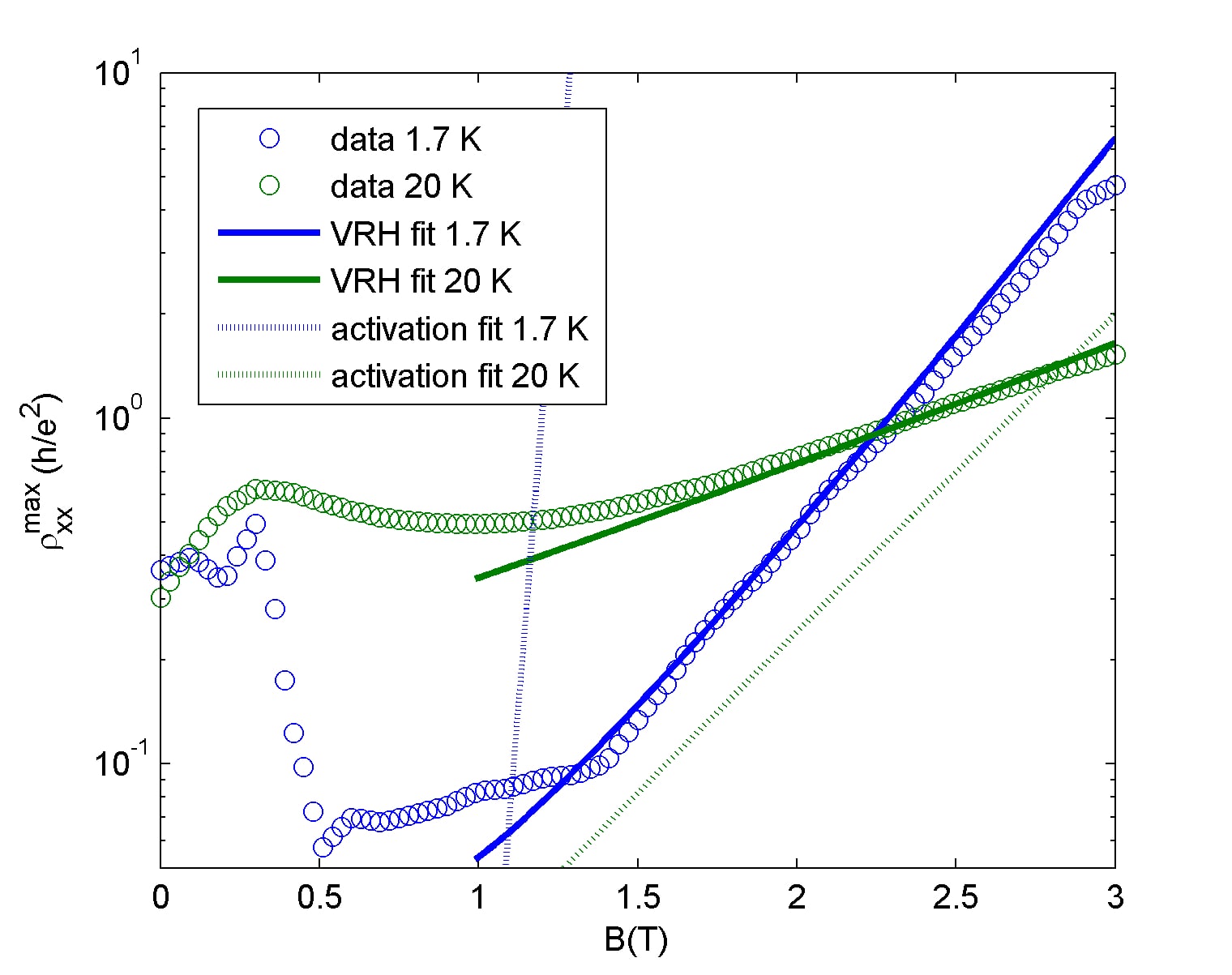
By contrast, the resistivity at T can be easily explained, qualitatively and quantitatively. Above T, the magnetoresistance increases almost exponentially. As the gap is theoretically proportional to , it means that the resistance increases exponentially with the gap.
First, a simple activation law cannot fit satisfactorily the data because the experimental temperature dependence of the resistivity is too small. The dotted lines in Fig. S5 show a tentative fit , where is half the theoretical gap. Obviously, the fit is very poor.
Second, For two-dimensional systems in the quantum Hall regime, variable range hopping (VRH) is often the dominant conduction mechanism. For VRH with a Coulomb gap, in the so-called Efros-Shklovskii VRH, (EF-VRH), the conductivity varies as . Here, is a fit parameter, which depends on the localization length as: where is the vacuum dielectric constant, is the relative dielectric constant, and 6.2 is a constant. From the scaling theory of the QHE, is expected to vary as , where , is the energy separation between the electrochemical potential and the LL delocalized states. Assuming is half the theoretical gap between the two zero mode LLs, EF-VRH can fit satisfactorily both and -dependence of the magnetoresistance, see Fig. S5. From the ES-VRH fit, one can tentatively extract the localization length: nm at T and nm at T.
Our results and our analysis suggest that VRH alone describes the transport not only on the Hall plateaus but also at the plateau transition, as originally suggested by Polyakov-Shklovskii Polyakov and Shklovskii (1993) and as recently observed in graphene Bennaceur et al. (2012). The good understanding of the transport properties around the normal gap allows us to use these data in confidence to get a better estimation of .
.5 E. Conductivity mechanisms in the TI gap
Conductivity mechanisms in the TI gap are more difficult to determine. Fig. S6 shows at T, K and K. A small insulating behavior is visible for the resistance maximum, as expected for bulk conductivity. As most reports point towards a spin relaxation length of 1 m König et al. (2007), it would be very unlikely to observe the conductivity of the topological edge states in our large sample. Let us study here the influence of counter propagating edge states through non local transport measurements. Let us first assume that the bulk conductivity is completely negligible, and that backscattering is forbidden between the edge states because of spin conservation. At each metallic contact, the two counter-propagating states equilibrate. The four-probe resistance is then given by:
| (3) |
where , and are the respective numbers of floating contacts along the upper edge, along the lower edge and between the two (local or non-local) probes located on the lower edge. The exponent indicates that no backscattering takes place along the two edge states in the QW.
If backscattering takes places along the edge states with a typical length , the upper equation becomes:
| (4) |
where , are the lengths of the upper and lower edges and is the distance between the two voltage probes.
When the current is injected between contacts 12 and 4 and voltage measured between contacts 1 and 3 (see Fig. 1 in the main text), =5, =3, =1. This gives and for m. The last estimation for is very large. More realistic values would considerably increase the resistance. Therefore, the two above equations give the minimal value for the non local resistance when the conduction is driven only by edge states. Experimentally, we found at K, T and V (the resistance maximum). This is three orders of magnitude smaller than the previous expectations based on edge states.
By contrast, the classical van der Pauw current spreading also gives non local resistances. For the non- local configuration, this ohmic contribution is given by the formula:
| (5) |
As for this pair of contacts, using in this formula the measured value , we get , which is very close to the value given by the local experimental resistance . We conclude that the resistance is largely dominated by the bulk contribution, in both local and non-local configurations (for completeness, Eqs. 3 and 4 give and .
Finally, a linear magnetoresistance appears at V, around 20–30 K and below T. This gives rise to an apparent dip in the resistance in Fig. 3(g-h) of the main text. We speculate that this behavior is due to a quantum magnetoresistance effect, as proposed for materials with zero bandgap and linear dispersion Abrikosov (1998). In this scenario, the linear magnetoresistance is another signature of the closure of the gap around 20–30 T.
.6 F. Bernevig-Hughes-Zhang Hamiltonian
To describe the band inversion in HgTe/Cd(Hg)Te QWs, in which the first electron-like E1 and hole-like H1 subbands are very close in energy, one can also use the effective Dirac-type Bernevig-Hughes-Zhang (BHZ) Hamiltonian Bernevig et al. (2006), proposed for the electronic states in the vicinity of the point of the Brillouin zone. The latter is derived from the Kane Hamiltonian Krishtopenko et al. (2016a), which includes , , bulk bands with the confinement effect. Within the representation defined by the basis states E1,+, H1,+, E1,-, H1,-, the effective 2D Hamiltonian has the form:
| (6) |
where asterisk stands for complex conjugation, is the momentum in the QW plane, and
| (7) |
,
Here, is a 22 unit matrix, are the Pauli matrices, , , , and . The structure parameters , , , , depend on , Cd concentration in the barrier and external conditions (pressure, temperature, etc.). The sign of mass parameter describes inversion between E1 and H1 subbands: corresponds to a trivial state, while, for a QSHI state, . We note that has a block-diagonal form because the terms, which break inversion symmetry and axial symmetry around the growth direction, are being neglected Krishtopenko et al. (2016a). The latter is a quite good approximation for symmetric HgTe QWs.
To calculate Landau levels (LLs) in the presence of an external magnetic field oriented perpendicular to the QW plane, one should make the Peierls substitution, , where in the Landau gauge . Additionally, we add the Zeeman term in the Hamiltonian
| (8) |
where is the Bohr magneton, and are the effective (out-of-plane) g-factors of the E1 and H1 subbands, respectively.
Solving the eigenvalue problem for the upper block of , the LL energies are found analytically König et al. (2007):
| (9) |
For the lower block upper block of , the LL energies are written as
| (10) |
Here is the magnetic length given by . The LLs with energies and are called the zero-mode LLs König et al. (2007). They split from the edge of E1 and H1 subbands and tend toward conduction and valence band, respectively. The crossing of the zero-mode LLs occurs at a critical magnetic field (see Fig. 2 in the main text), above which the inverted band ordering is transformed into the trivial one König et al. (2007). One can show that for HgTe QWs with inverted band structure ().
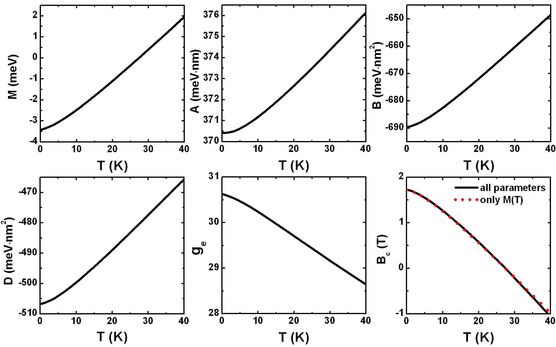
By using the 8-band Kane Hamiltonian, accounting interaction between the , and bands in zinc-blend materials, with temperature-dependent parametersKrishtopenko et al. (2016a) and by applying the procedure, described in Krishtopenko et al. (2016b), we have calculated the values of , , , , , and for our sample at different temperatures (see Fig. S7).
Figure S7 also shows a critical magnetic field as a function of temperature . The solid black curve represents the calculations performed within the Kane Hamiltonian Krishtopenko et al. (2016a). We note that the calculation of based on Eqs. (9) and (10), performed by taking into account temperature dependence of all parameters in the BHZ Hamiltonian, coincides with the values within the Kane model. The dotted red curve corresponds to the calculation of within the BHZ model if we take into account only temperature dependence of the mass parameter . The small difference between the curves means that temperature dependence of is mostly caused by temperature dependence of the band gap in our sample (see also Fig. 2 in the main text), while the temperature effect on the dispersion of the zero-mode LLs is negligible.
References
- Dykhne and Ruzin (1994) A. M. Dykhne and I. M. Ruzin, Phys. Rev. B 50, 2369 (1994).
- Shahar et al. (1997) D. Shahar, D. Tsui, M. Shayegan, E. Shimshoni, and S. Sondhi, Phys. Rev. Lett. 79, 479 (1997).
- Polyakov and Shklovskii (1993) D. G. Polyakov and B. I. Shklovskii, Phys. Rev. Lett. 70, 3796 (1993).
- Bennaceur et al. (2012) K. Bennaceur, P. Jacques, F. Portier, P. Roche, and D. C. Glattli, Phys. Rev. B 86, 085433 (2012).
- König et al. (2007) M. König, S. Wiedmann, C. Brüne, A. Roth, H. Buhmann, L. W. Molenkamp, X.-L. Qi, and S.-C. Zhang, Science 318, 766 (2007).
- Abrikosov (1998) A. Abrikosov, Phys. Rev. B 58, 2788 (1998).
- Bernevig et al. (2006) B. A. Bernevig, T. L. Hughes, and S.-C. Zhang, Science 314, 1757 (2006).
- Krishtopenko et al. (2016a) S. S. Krishtopenko, I. Yahniuk, D. B. But, V. I. Gavrilenko, W. Knap, and F. Teppe, Phys. Rev. B 94, 245402 (2016a).
- Krishtopenko et al. (2016b) S. S. Krishtopenko, W. Knap, and F. Teppe, Sci. Rep. 6, 30755 (2016b).