Experimental search for the origin of low-energy modes in topological materials
Abstract
Point-contact spectroscopy of several non-superconducting topological materials reveals a low-temperature phase transition that is characterized by a Bardeen-Cooper-Schrieffer-type of criticality. We find such a behavior of differential conductance for topological surfaces of non-magnetic and magnetic Pb1-y-xSnyMnxTe. We examine a possible contribution from superconducting nanoparticles, and show to what extend our data are consistent with Brzezicki’s et al. theory [arXiv:1812.02168] assigning the observations to a collective state adjacent to atomic steps at topological surfaces.
Introduction. A series of point-contact experiments has revealed the existence of low-energy modes at junctions of metal tips with topological semiconductors and semimetals Das et al. (2016); Aggarwal et al. (2016); Wang et al. (2016); Aggarwal et al. (2017); Wang et al. (2017, 2018); Naidyuk et al. (2018); Shvetsov et al. (2019); Zhu et al. (2018). Surprisingly, despite the absence of global superconductivity in these systems, the features in d/d decay critically with temperature and the magnetic field in accord with the Bardeen-Cooper-Schrieffer (BCS) theory. It has, therefore, been concluded that the superconductivity results from tip-induced strain. In the case of Cd3As2 this interpretation appears to be supported by the featureless spectrum in the case of a soft point-contact produced by silver paint Wang et al. (2016, 2018). Surprisingly, however, Andreev reflection-type spectra were recently reported for Au/Cd3As2 junctions (with neither a four probe zero-resistance state nor the Meissner effect) Shvetsov et al. (2019), as well as for topological semimetals MoTe2 Naidyuk et al. (2018) and WC Zhu et al. (2018) with hard and soft point-contacts Naidyuk et al. (2018) of various nonmagnetic and magnetic metals Zhu et al. (2018). A timely question then arises about the properties of other materials, such as topological crystalline insulators (TCI) Fu (2011); Hsieh et al. (2012); Dziawa et al. (2012); Tanaka et al. (2012); Xu et al. (2012) in which hard point-contact characteristics reveal zero-bias conductance peaks (ZBCPs) Das et al. (2016).
Here we show, employing a soft point-contact method, that a conductance gap with a broad ZBCP or Andreev-type characteristics develop at junctions of Ag with topological surfaces of diamagnetic, paramagnetic, and ferromagnetic Pb1-y-xSnyMnxTe, where and , in which no signs of superconductivity are found. Nevertheless, the temperature dependence of the gap shows a BCS-like critical behavior as a function of temperature and the magnetic field with up to 4.5 K and up to 3 T independent of the orientation of the magnetic field with respect to the surface plane. This implies the emergence of a collective low-temperature phase whose appearance is insensitive not only to the magnetic state of the metallic part of the junction, as found previously Das et al. (2016); Zhu et al. (2018), but also to the magnetic character of the topological material. In order to elucidate the nature of these striking observations we put forward two models.
First, previous studies of the materials in question revealed superconductivity associated with metal nano-precipitates Darchuk et al. (1998) or misfit dislocations at the heterostructure interfaces Murase et al. (1986); Fogel et al. (2006). Furthermore, studies of Pb/(Pb,Sn)Te junctions point to the presence of Sn diffusion in Pb Buchner et al. (1979), which rises the question on whether such an effect could generate superconducting Pb or Sn at the interface. It might be also anticipated that strain associated with different thermal expansion coefficients of silver paint and the samples or hard tips could generate misfit dislocations or precipitates. However, a series of auxiliary high-sensitivity magnetization and resistance measurements as well as high-resolution structural investigations of our samples have not revealed the presence of superconducting nanoparticles within our experimental resolution.
Second, a possible origin of a local collective phase at topological surfaces has recently been proposed by Brzezicki, Wysokiński, and Hyart (BWH) Brzezicki et al. (2018), who noted that the electronic structure of one-dimensional (1D) states at atomic steps in TCIs, revealed by scanning tunneling microscopy Sessi et al. (2016); Iaia et al. (2018), is significantly richer than anticipated previously Sessi et al. (2016); Iaia et al. (2018); Polley et al. (2018); Rechciński and Buczko (2018). According to BWH, these 1D states may show a low-temperature Peierls-like instability leading to the appearance of low-energy excitations associated with topological states at the domains walls of the collective phase. We discuss to what extent our data are consistent with the BWH model and a possible microscopic nature of the collective phase.
Samples. We investigate here single crystals of rock salt Pb1-ySnyTe and Pb1-y-xSnyMnxTe obtained via the self-selecting vapor growth method Dziawa et al. (2012); Szczerbakow and Durose (2005) and the Bridgman technique Story et al. (1986), respectively. Results of electric, magnetic, x-ray, and electron transmission microscopy characterization of the studied samples are presented in the Supplemental Material SM . We study samples with , and 1, which covers both the topologically trivial and non-trivial range, as the TCI phase occurs for Xu et al. (2012). According to both angle-resolved photoemission Tanaka et al. (2012); Xu et al. (2012); Polley et al. (2016) and magnetotransport investigations Dybko et al. (2017), the surface topological cones coexist with bulk states even for high bulk carrier densities specific to these systems. At the same time, the energetic position of the surface-cone neutrality points with respect to the Fermi level depends on the character of the surface states and the degree of surface oxidation, the question under investigations now Berchenko et al. (2018); Chang et al. . The search for metal precipitates by x-ray diffraction and electron microscopy, also in the vicinity of dislocations, has not revealed the presence of any nanoclustering within the state of the art resolution SM .
According to the results of magnetization measurements SM , carried out by employing a superconducting quantum interference device (SQUID), non-magnetic compounds show a field-independent diamagnetic susceptibility, enhanced by strong interband polarization in the inverted band structure case. The Mn-doped samples contain a Sn concentration corresponding to the TCI phase and a bulk hole density high enough to populate 12 valleys. A large density of states (DOS) associated with these valleys makes hole-mediated exchange coupling between Mn ions sufficiently strong to drive the ferromagnetic ordering Story et al. (1986); Swagten et al. (1988). The Curie temperature , separating the paramagnetic and ferromagnetic phase, is 2.7 and 14 K for the Mn concentration and 0.10, and Sn content and 0.74, respectively SM . These values are consistent with the mean-field – Zener model Dietl et al. (2000); Dietl and Ohno (2014); SM .
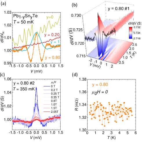
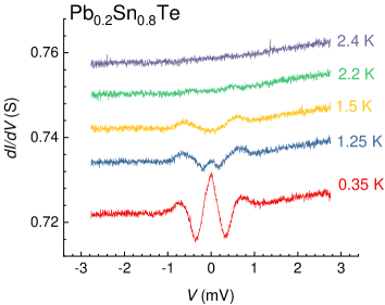
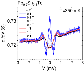
Point-contact spectroscopy. We employ the soft point-contact method Daghero and Gonnelli (2010); Sasaki et al. (2011, 2012), in which a 15 m Au wire is fixed by silver paint. As shown in Fig. 1(a), d/d is featureless in the case of the topologically trivial materials PbTe and Pb0.80Sn0.20Te. However, in the case of the diamagnetic TCI Pb0.20Sn0.80Te we find at low temperatures and magnetic fields maxima (ZBCP) centered at and superimposed on a conductance gap (see also data Ref. SM, ). As observed in other systems Das et al. (2016); Aggarwal et al. (2016); Wang et al. (2016); Aggarwal et al. (2017); Wang et al. (2017, 2018); Shvetsov et al. (2019); Zhu et al. (2018), the spectra form vary from contact to contact SM . In the thermal regime they change over time in a jump way as well as can be modified by current pulses across the point contact SM ; Daghero and Gonnelli (2010).
Within the point-contact theories Daghero and Gonnelli (2010), the enhanced junction conductance at and at , i.e., the presence of ZBCP, can be interpreted in terms of the Andreev reflection (pointing to superconductivity) or to enlarged DOS due to the appearance of, for instance, zero modes at Brzezicki et al. (2018). In either of these scenarios current heating at higher bias voltages may result in side minima Sheet et al. (2004). Within the superconductivity models, such a spectrum is typical for the thermal regime, i.e., when the contact diameter is larger than the inelastic diffusion length Daghero and Gonnelli (2010) [Fig. 1(c)]. In the opposite limit, spectroscopic information is not blurred, and side maxima in d/d, reflecting the DOS enlargement at the gap edges, provide the value of the relevant gap. Within such an approach the data in Fig. 1(b) (see also the data in Ref. SM ), correspond to the spectroscopic regime. An interesting question arises on whether such a phenomenology can be directly applied to other gaped collective states, such as the one proposed by BWH Brzezicki et al. (2018).
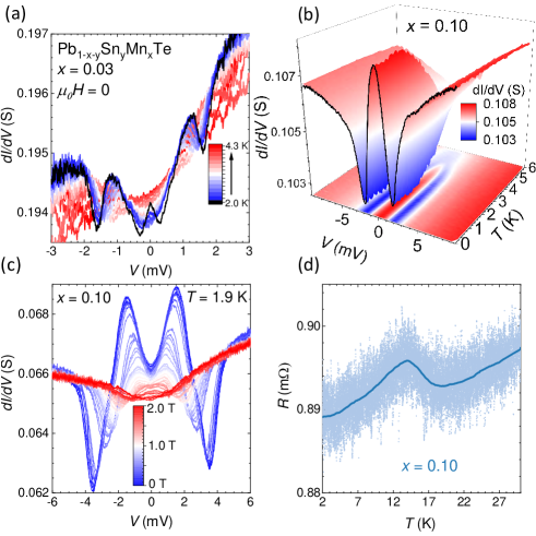
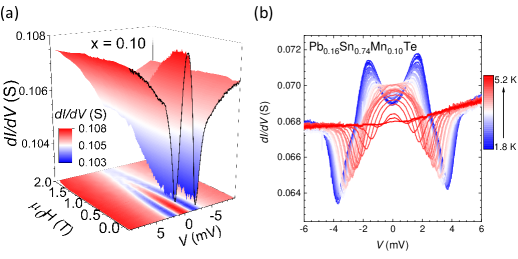
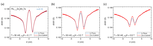
According to Fig. 2, d/d shows clear spectroscopic features in magnetic crystals. The spectrum for Pb0.3Sn0.67Mn0.03Te [Fig. 2(a)] exhibits a gap with a small zero-bias peak vanishing smoothly with increasing temperature. For a cleaved (100) surface of Pb0.16Sn0.74Mn0.10Te, a splitting of ZBCP, resembling Andreev reflection characteristics in the spectroscopic regime and for a non-zero barrier transparency Daghero and Gonnelli (2010) has been detected [Fig. 2(c)].
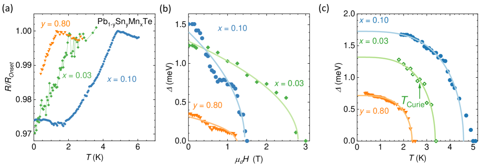
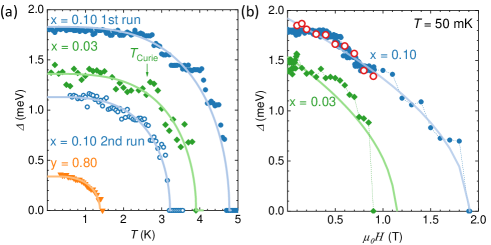
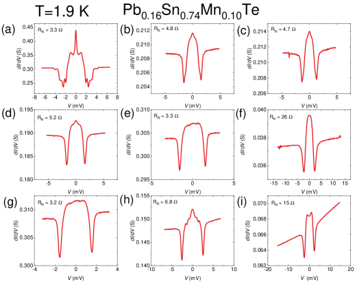
Importantly, temperature and magnetic field ranges in which these spectroscopic features appear are rather enhanced compared to non-magnetic crystals. This is best seen in Fig. 3 that depicts the contact resistance and a half of the energy distance between conductance maxima, for all studied samples with high Sn content. Furthermore, according to Fig. 3, is quite well described by an interpolation formula of the BCS expression, , where in our case is more than twofold greater than the BCS value . Similarly, a reasonable account of data is obtained by using another interpolation formula suitable for type II superconductors, . This description of holds for the diamagnetic Pb0.2Sn0.80Te, ferromagnetic Pb0.16Sn0.74Mn0.10Te, and across the paramagnetic–ferromagnetic phase boundary, the case of Pb0.20Sn0.67Mn0.03Te, in which . The existence of a transition to another phase is also documented by a kink in the temperature dependence of the differential resistance for at , as shown in Fig. 3(a).
The accumulated results demonstrate, therefore, the appearance in junctions of the normal metal with diamagnetic, paramagnetic, and ferromagnetic IV-VI TCIs of another phase below and , which is characterized by an energy gap and excitations residing near its center. The presence of a phase transition rules out the Kondo effect Appelbaum (1966); Anderson (1966); Meir et al. (1993); Pustilnik and Glazman (2001) and the Coulomb gap Efros and Shklovskii (1975); Al’tshuler and Aronov (1979) as the mechanisms accounting for the observed features. Similarly, the absence of the global superconductivity without metal layers [Figs. 1(d) and 2(d) as well as data in Ref. SM, ] indicate that unconventional 2D superconductivity associated with surface topological states Kundu and Tripathi (2017) or dislocation arrays Tang and Fu (2014) in TCIs does not appear under our experimental conditions. The absence of 2D superconductivity is also documented by similar values of for the magnetic field perpendicular and parallel to the surface SM .
Role of superconducting precipitates. According to comprehensive structural and SQUID studies, magnetic nanoparticles account for high ferromagnetism observed in a number of semiconductors and oxides over the last two decades Dietl et al. (2015). Similarly to the ferromagnetic case, embedded nanoparticles can show a variety of superconducting characteristics, such as the Meissner effect, which may depend on nanoparticle chemical composition, strain, and size Darchuk et al. (1998); Murase et al. (1986); Fogel et al. (2006); Li et al. (2003); Yeh et al. (2008). Here, the presence of superconducting precipitates that could give rise to local superconductivity is ruled out, within an experimental accuracy of 0.1 ppm, by high-sensitivity beyond state-of-the-art SQUID magnetometry SM ; Gas and Sawicki (2019). Furthermore, no precipitates have been revealed by state-of-the-art x-ray diffraction and transmission microscopy measurements SM . Similarly, no indications of superconductivity have been found in topological samples covered entirely by silver paint or containing a deposited silver film SM , pointing to the absence of both interfacial superconductivity and superconducting inclusions at the metal/semiconductor interface.
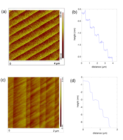
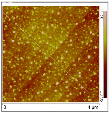
Role of surface atomic steps. Figure 4 presents the surface morphology of our single crystals under ambient conditions, determined by atomic force microscopy (AFM). As seen in Figs. 4(a,b), (001) facets of as grown Pb0.20Sn0.80Te contain atomically flat 0.5 m wide terraces, terminated by monoatomic steps. Similarly, Figs. 4(c,d) visualize a (001) surface of cleaved Pb0.16Sn0.74Mn0.10Te showing larger roughness and multilayer steps. Results in Figs. 1(b,c) and 2(c) were actually taken for these two surfaces, respectively. We claim that a collective low-temperature phase of the carrier liquid occupying 1D topological step states Sessi et al. (2016); Brzezicki et al. (2018); Polley et al. (2018); Rechciński and Buczko (2018); Iaia et al. (2018) may account for the differential conductance spectra reported here. According to AFM micrographs, a single Ag grain extends over a dozen of steps. The magnitude of ZBCP, about 50 to , is consistent with the fact that several grains participate in the charge transport process.
The above interpretation requires the Fermi level of our -type samples to reside within the 1D states, whereas tight-binding computations place the 1D band in the gap Sessi et al. (2016); Brzezicki et al. (2018); Polley et al. (2018); Rechciński and Buczko (2018); Iaia et al. (2018). We note, however, that our experimental method implies the formation of Schottky’s metal-semiconductor junction, which leads usually to the Fermi level pinning in the band gap region at the semiconductor surface Tung (2014). This effect, together with a considerable width of the 1D band, as predicted by the BWH theory Brzezicki et al. (2018), make the partial occupation of the 1D states plausible. The depletion in the bulk carrier density implies also that Mn spins adjacent to the surface will be rather coupled by antiferromagnetic superexchange Górska and Anderson (1988) than by the hole-mediated ferromagnetic interactions dominating in the bulk Story et al. (1986); SM .
However, since the Fermi liquid is unstable in the 1D case, one expects the emergence of a collective state at low temperatures driven by carrier correlation, presumably enhanced by coupling to phonons and localized spins. For a class of electronic instabilities, such as superconductivity and charge/spin density waves, the BCS relation between the gap and the critical temperature remains valid within the mean-field approximation. However, because of the dominating role played by thermal and quantum fluctuations of the order parameter, the apparent magnitude of becomes much reduced in the 1D case Arutyunov et al. (2008); Pouget (2016). This explains the enhanced magnitude of over the BCS value (Fig. 3) but indicates also that 1D surface states may not support superconductivity with as high as 5 K.
As demonstrated by BWH Brzezicki et al. (2018), the 1D states adjacent to the surface atomic step show much more abundant spectrum than anticipated previously Sessi et al. (2016); Polley et al. (2018); Rechciński and Buczko (2018); Iaia et al. (2018). Within this insight, the effects of magnetic instabilities have been considered and the nature of low-energy excitations proposed Brzezicki et al. (2018). In an analogy with the Su–Schrieffer–Heeger model Heeger et al. (1988), the low-energy modes are associated with domain walls between the regions characterized by the opposite directions of the order parameter for which, as proven, topological invariants differ. These walls, and thus, low energy excitations vanish in the magnetic field with a rate determined by a competition of the carrier-carrier exchange coupling with the Zeeman, spin-orbit, and – exchange interactions. Depending on the assumed broadening, the evaluated conductance spectra show a single ZBCP, or a more complex peak structure that reflects the multi-mode excitation spectrum and may resemble Andreev reflection Brzezicki et al. (2018).
Summary and outlook. Our results on soft point-contact spectroscopy bring into light the existence of a low-temperature phase in lead-tin and lead-tin-manganese tellurides with tin content corresponding to the topological phase, which substantiates the universality of the phenomenon Das et al. (2016); Aggarwal et al. (2016); Wang et al. (2016); Aggarwal et al. (2017); Wang et al. (2017, 2018); Shvetsov et al. (2019); Zhu et al. (2018). The findings could be explained by the presence of superconducting nanoparticles, the surface topological states playing only an ancillary role. However, no indications for the formation of nanoparticles have so far been found. At the same time, our experiments do not provide evidence for the presence of superconductivity at the interface between the metal and the TCI. Hence, this phase can be also linked to carries occupying 1D topological states adjacent to surface atomic steps, which undergo a transition to a collective state at sufficiently low temperatures and magnetic fields. Four microprobe measurements of conductance along individual steps in materials with the Fermi level within the step states are expected to demonstrate whether this collective phase is a 1D superconductor or a 1D gaped insulator with low-energy excitations at the domain walls. Future work will show to what extent the unusual properties associated with the presence of 1D and 0D topological states offer new and hitherto unexplored functionalities.
Acknowledgements. We thank Marek Foltyn and Pawel Skupinski for technical support and Victor Galitski for a valuable discussion. The Research Foundation MagTop – International Centre for interfacing Magnetism and Superconductivity with Topological Matter (short name: International Research Centre MagTop) is funded by the Foundation for Polish Science through the IRA Programme financed by theEU within SG OP Programme. The work at the Institute of Physics, Polish Academy of Sciences was supported by the National Science Center (Poland) through the following grants: PRELUDIUM (2015/19/N/ST3/02626), OPUS (2012/07/B/ST3/03607, 2013/09/B/ST3/04175, 2014/15/B/ST3/03833, 2017/27/B/ST3/02470), and MAESTRO (2011/02/A/ST3/00125). The TEM/FIB investigation was performed on equipment supported by Polish Government under Agreement 4277/E-67/SPUB/2017/1.
Supplemental Information
S1 Studied samples
Table I presents information on the studied samples.
| Sample | (cm-3) | (cm2/Vs) |
|---|---|---|
| PbTe | 970 | |
| Pb0.80Sn0.20Te | 280 | |
| Pb0.20Sn0.80Te | 80 | |
| SnTe | 350 | |
| Pb0.30Sn0.67Mn0.03Te | 110 | |
| Pb0.16Sn0.74Mn0.10Te | 180 |
S2 Search for precipitates by x-ray diffraction
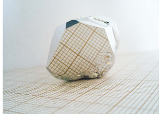
For our experiments we prepared dedicated bulk crystals of the highest, currently available, quality. Our SnTe and Pb0.2Sn0.8Te crystals were grown by self-selecting vapor growth (SSVG) method known to provide large (volume of the order of 1 cm3) single crystals with dominant (001) and additional (111) crystal facets (see photo in Fig. S1). The SSVG growth involves vapor transport in the presence of a small temperature gradient at temperatures slightly below the melting point, and provides IV-VI semiconductor crystals of excellent crystal quality, good chemical homogeneity with a relatively small deviation from stoichiometry, and free from detectable inclusions of foreign crystal phases.
Due to low vapor pressure of Mn, the growth of magnetic Pb0.16Sn0.74Mn0.10Te crystals requires the application of the Bridgman method, i.e., crystallization from a melt. Although crystalline grains are here much smaller (typical dimension 0.5 mm) they are only slightly misoriented (0.06o). The uniformity of both carrier density and ferromagnetic properties point to the homogeneity of the chemical composition.
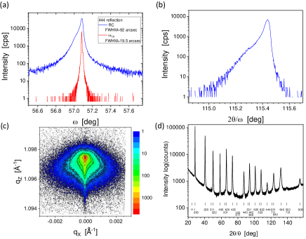
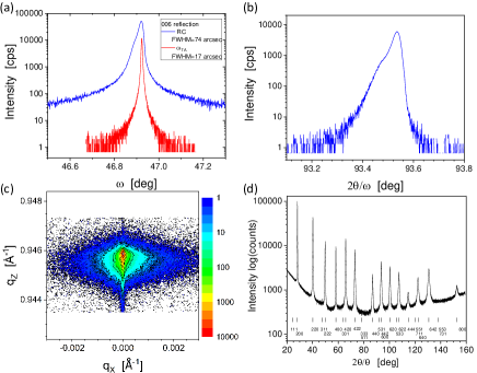
The crystallographic quality of the samples has been assessed by the-state-of-the-art high-resolution x–ray diffraction (HR-XRD) and powder diffraction. The , 2/ scans, and reciprocal space maps (RSM) have been collected for reflection 444 (SnTe and Pb0.16Sn0.74Mn0.10Te) and 006 (Pb0.20Sn0.80Te), as shown in Figs. S2, S3 and S4, respectively. For the crystals of SnTe and Pb0.2Sn0.8Te grown by the SSVG method one finds very sharp diffraction peaks fully accounted for by a single-rock salt crystal phase. The application of various XRD geometries (as indicated in Figs. S2 and S3) permitted the determination of the RC width parameters of 92 and 74 arcsec for SnTe and Pb0.2Sn0.8Te, respectively. After correcting for diffraction peaks asymmetry and background contribution due to diffusive scattering by native defects (vacancies) present in the crystals we could also evaluate the crystal perfection of (111) and (001) planes as given by the RC width parameter 17-19.5 arcsec. One may notice that this magnitude of the RC parameters are observed for good GaAs (001) crystals.
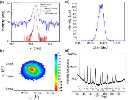
In the case of Pb0.16Sn0.74Mn0.10Te - the planes (111) were inclined at the angle of 25o to the surface, so that 444 was asymmetrical (the x–ray beam geometry at a high angle to the sample was used). The Pb0.16Sn0.74Mn0.10Te sample consists of slightly misoriented mm2 single crystalline grains. The mean grain deviation angle is estimated to be . For an x–ray beam limited by a mask and slit of such dimensions, the single crystal diffraction pattern is observed (Fig. S4).
| Sample | a () |
|---|---|
| Pb0.20Sn0.80Te | 6.3426(3) |
| SnTe | 6.3129(3) |
| Pb0.16Sn0.74Mn0.10Te | 6.3098(5) |
Wide-angle x-ray power diffraction for used to detect foreign crystallographic phases in the studied samples. The data collected in Figs. S2(d), S3(d), and S4(d) were taken with excellent statistics, peak-to-background ratio 74, and in a broad angular range ( up to 159o). The positions of all peaks point to the rock salt crystal symmetry (Fm3-m) with no indication for the presence of a secondary phase. The determined lattice parameters are given in the Table II.
S3 Search for precipitates by electron microscopy
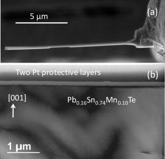
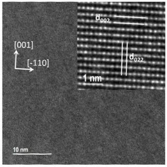
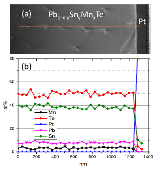
Figure S5(a) shows scanning electron microscopy (SEM) image of a lamella prepared of Pb0.16Sn0.74Mn0:10Te for transmission electron microscopy (TEM) studies. A m defect-free area is presented in Fig. S5(b). The dark wavy features are due to lamella bending. The sharp feature seen at the bottom right corner is caused by mechanical deformation that occurred during the thinning process or by processing of the crystal during previous investigations. Structural defects (mainly small dislocation loops) can be found is some regions near the surface of the crystal - no deeper than 2 m from the surface. No fluctuations of elemental composition or precipitations of other phases are detected. It appears that Pb and Mn atoms substitute the Sn atoms without ordering or segregation that could be detected within our sensitivity. The high-resolution TEM (HRTEM) image (Fig. S6) indicates a perfect cubic lattice visible in [110] zone axis. A quantitative profile of the crystal region containing structural defects (dislocations) near the surface zone obtained by energy dispersive x-ray spectroscopy (EDS) is presented in Fig. S7. No aggregation of particular constituents is detected, as composition fluctuations are within the error bar of the method. The determined atomic concentrations of the constituting elements are in good agreement with results of our SQUID measurements and specifications found in the previous characterization studyS7.
S4 Magnetic properties
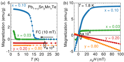
According to results of magnetization measurements collected in Fig. S9, non-magnetic compounds show field-independent diamagnetic susceptibility, enhanced by strong interband polarization in the inverted band structure case. The Mn-doped samples contain Sn concentration corresponding to the TCI phase and the hole density high enough to populate twelve valleys. A large density of states (DOS) associated with these valleys makes hole-mediated exchange coupling between Mn ions sufficiently strong to drive the ferromagnetic ordering Story et al. (1986); Swagten et al. (1988). As shown in Fig. S9, the Curie temperature , separating the paramagnetic and ferromagnetic phase, is 2.7 and 14 K for the Mn concentration and 0.10, and the Sn content and 0.74, respectively.
According to the mean-field Zener model Dietl et al. (2000); Dietl and Ohno (2014)
| (1) |
where and take into account the presence of short-range antiferromagnetic interactions, and is the cation concentration. Important effects of spin-orbit interactions, carrier-carrier correlation, and mixing between anion and cation wave functions are incorporated into an effective exchange integral . In order to evaluate its magnitude we take Mn spin and DOS of holes at the Fermi level from specific heat measurements for Sn1-zInzTe with comparable hole densities Novak et al. (2013). The values of and 0.095 are determined from the Curie constant obtained from our magnetic susceptibility measurements between 100 K and ; , where K (Ref. Górska and Anderson, 1988). For the experimental magnitudes of we then obtain eV, a value at the upper bound of those determined for Mn-doped lead chalcogenides Dietl et al. (1994).
S5 Search for superconducting precipitates by SQUID magnetometry
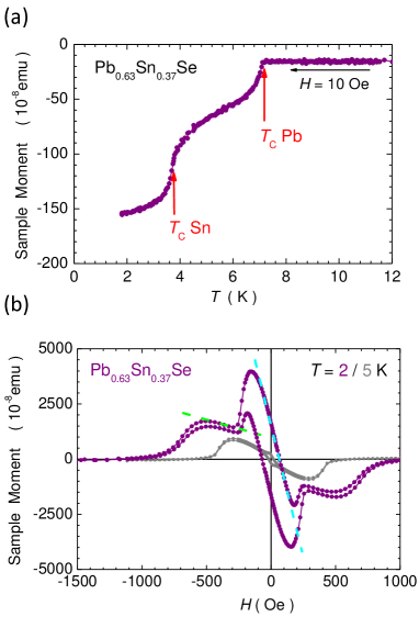
We assess the presence of superconducting Pb, Sn, and related precipitates in samples of topological Pb0.20Sn0.80Te and non-topological Pb0.80Sn0.20Te, discussed in the main body of the paper, by SQUID magnetometry. We start by discussing results of magnetization measurements for a reference sample Pb0.63Sn0.37Se. As shown in Fig. S10, two clear diamagnetic steps in the temperature and magnetic field dependencies of magnetization are recorded, quite accurately corresponding to Pb and Sn superconducting transition temperatures 7.2 and 3.7 K as well as critical magnetic fields at 2 K, 700 and 250 Oe, respectively. The presence of magnetic hystereses points to some pinning. Assuming a spherical shape of precipitates, the field derivative of the magnetic moment assumes the form,
| (2) |
where , , and are mass, density, and the experimentally established slopes corresponding to Pb or -Sn. From the experimental slopes , depicted in Fig. S10(b), we obtain precipitation masses of g and g, which lead to the weight fraction of precipitates %, as sample weight is 38 mg.
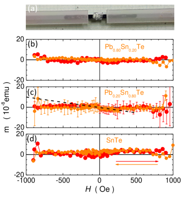
Neither Pb0.20Sn0.80Te nor Pb0.80Sn0.20Te shows such a signal. We assign a large concentration of Sn and Pb precipitates in Pb0.63Sn0.37Se to the fact that Sn content is close the solubility limit . In order to test our telluride samples Pb1-ySnyTe with even higher sensitivity and, in particular, to compensate a relatively large bulk diamagnetic signal, a dedicated sample holder has been prepared. As illustrated in Fig. S11(a), 20–40 mm long and 5 mm wide strips of sapphire are glued to the silicon sample holder Gas and Sawicki (2019) forming in the holder center a gap of the length of about 5 mm, to which studied samples are inserted [Fig. S11(a)]. As these sapphire strips extend from the gap for about 8 cm each way, by adjusting the mass of measured samples to be inserted into the gap, the total signal can be made field independent (typically down to 2% of the initial slope), provided that both the sample and the sapphire stripe do not contain any magnetic or superconducting inclusions. We use a pure GaAs sample to determine a background signal of the sample holder. By adjusting masses of Pb1-ySnyTe samples of interest here, and after correcting for sapphire responseS5, we obtain SQUID signals presented in Fig. S11(b–d). The magnitude of noise indicates that for a mean mass of our samples, i.e., 60 mg, the upper limit of the weight fraction of precipitates that could give a response of the type presented in Fig. S11 is 0.1 ppm.
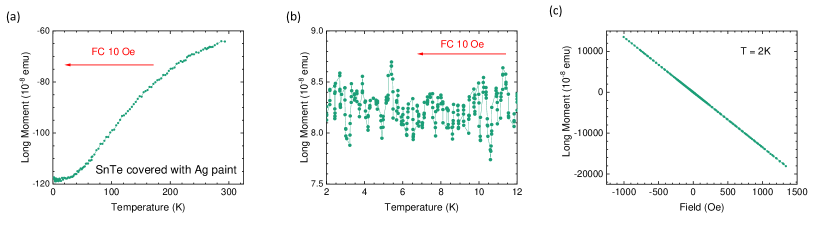
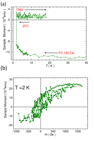
It can be hypothesized that silver paint employed for point contact spectroscopy contains superconducting precipitates which might account for the observed features in differential conductance. This scenario is excluded by magnetization measurements of silver paint deposited on a Si sample presented in Fig. S12. A signal from residual paramagnetic impurities superimposed on a temperature independent diamagnetic response is found. Furthermore, considering a possible diffusion of Sn or Pb towards the Ag electrode or the dislocation formation by the temperature stress, the magnetic response of the SnTe sample with the topological surface covered entirely by silver paint has been measured by SQUID magnetometry. As shown in Fig. S13, no superconductive features are detected down to the lowest accessible temperature of 2 K.
S6 Resistance and differential conductance of Ag/TCI and Au/TCI interfaces
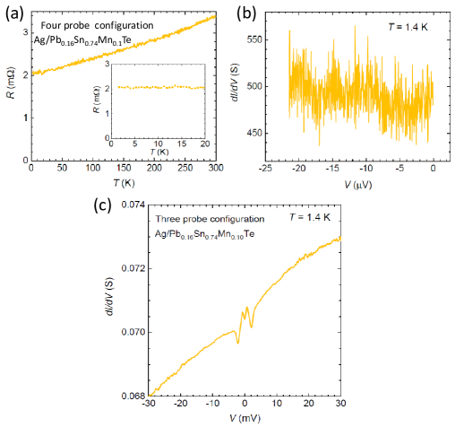
Our point-contact spectroscopy experiments have been performed by using silver paint. The remaining two contacts are spot-welded into the sample to ensure a good electrical connection. To check properties of the Ag/TCI interface we have deposited a 50 nm layer of Ag using ultra high vacuum e-beam evaporator onto a ferromagnetic Pb0.16Sn0.74Mn0.10Te sample. Resistance measurements of the Ag/TCI bilayer have been carried out employing a four probe configuration with the current probes spot-welded to the sample and the voltage probes fixed by silver paint to the silver layer. The resistance measurements as a function of temperature [Fig. S14(a)] and bias voltage [Fig. S14(b)] do not exhibit any noticeable superconductivity in the studied temperature and bias voltage ranges. At the same time, in the three contact geometry, with one of the silver paint contacts serving as a current and voltage probe, we detect a ZBCP, as shown in Fig. S14(c). Thus we conclude that the presence of the ZBCP is not accompanied by a superconductivity of the Ag/TCI interface. Furthermore, a point contact spectroscopy experiment is performed by using only spot-welded contacts. No features in differential conductance are found, as show in Fig. S15. This indicates that no ZBCP appears if the interface is damaged by the welding process.

S7 Additional data on point contact spectroscopy
Figure S16 supplements data presented in the Fig. 2 in the main text. Figure S17 presents dependence of the gap, interpreted as a differential conductance minimum, on temperature (a) and the magnetic field (b) in the thermal regime. This is to support the data presented in the Figs. 3(b,c) in the main text. Figure S18 shows how spectroscopic features vanish as a function of temperature. First, the zero-bias peak decreases as a function of temperature, leaving clear gapped spectrum at 1.5 K. Similarly, the magnetic field quenches zero-bias peak as depicted in Fig. S19.
S8 Magnetic anisotropy of differential conductance
In order to probe magnetic anisotropy of the point-contact spectra, differential conductance of the Pb0.16Sn0.74Mn0.10Te sample has been measured for various fields perpendicular and parallel to the sample surface. As seen in Fig. S20 there is some anisotropy in the peak heights but no noticeable differences in the width of the spectra. A minor magnitude of magnetic anisotropy reemphasizes that the observed low temperature phase has no global 2D character.
S9 Effect of current pulses
In most cases freshly prepared silver paint contacts reveal zero-bias conductance peak in topologically non-trivial samples. However, some of the contacts stopped working after temperature sweeps or showed no structure during initial measurements. We have found, as could be expected for phenomena relying on properties of surface steps, that characteristics of differential conductance spectra in topological samples can be modified by current pulses, as shown in Fig. S21(a). A typical pulse sequence consists of 1 ms pulses with amplitude 100 mA, with the repetition rate of 10 Hz. Such a sequence does not awake any structure in conductance of non-topological Pb0.80Sn0.20Te [Fig. S21(b)].
S10 AFM scans after point-contact spectroscopy studies
Figure S23 presents the AFM image of the (011) surface obtained by a wire-saw cut and subject to a series of etchings. As seen surface roughness are significantly larger compared to the freshly grown or cleaved surfaces, whose AFM images are presented in Fig. 4 of the main text.
References
- Das et al. (2016) S. Das, L. Aggarwal, S. Roychowdhury, M. Aslam, S. Gayen, K.a Biswas, and G. Sheet, “Unexpected superconductivity at nanoscale junctions made on the topological crystalline insulator Pb0.6Sn0.4Te,” Appl. Phys. Lett. 109, 132601 (2016).
- Aggarwal et al. (2016) L. Aggarwal, A. Gaurav, G. S. Thakur, Z. Haque, A. K. Ganguli, and G. Sheet, “Unconventional superconductivity at mesoscopic point contacts on the 3D Dirac semimetal Cd3As2,” Nat. Mater. 15, 32–37 (2016).
- Wang et al. (2016) He Wang, Huichao Wang, Haiwen Liu, Hong Lu, Wuhao Yang, Shuang Jia, Xiong-jun Liu, XC Xie, Jian Wei, and Jian Wang, “Observation of superconductivity induced by a point contact on 3D Dirac semimetal Cd3As2 crystals,” Nat. Mater. 15, 38 (2016).
- Aggarwal et al. (2017) L. Aggarwal, S. Gayen, S. Das, R. Kumar, S. Vicky, C. Felser, C. Shekgar, and G. Sheet, “Mesoscopic superconductivity and high spin polarization coexisting at metallic point contacts on Weyl semimetal TaAs,” Nat. Commun. 8, 13974 (2017).
- Wang et al. (2017) He Wang, Huichao Wang, Yuqin Chen, Jiawei Luo, Zhujun Yuan, Jun Liu, Yong Wang, Shuang Jia, Xiong-Jun Liu, Jian Wei, and Jian Wang, “Discovery of tip induced unconventional superconductivity on Weyl semimetal,” Sci. Bull. 62, 425 – 430 (2017).
- Wang et al. (2018) He Wang, Lei Ma, and Jian Wang, “Tip-induced or enhanced superconductivity: a way to detect topological superconductivity,” Sci. Bulletin 33, 1141–1158 (2018).
- Naidyuk et al. (2018) Y. Naidyuk, O. Kvitnitskaya, D. Bashlakov, S. Aswartham, I. Morozov, I. Chernyavskii, G. Fuchs, S.-L. Drechsler, R. Hühne, K. Nielsch, B. Büchner, and D. Efremov, “Surface superconductivity in the Weyl semimetal MoTe2 detected by point contact spectroscopy,” 2D Mater. 5, 045014 (2018).
- Shvetsov et al. (2019) O. O. Shvetsov, V. D. Esin, A. V. Timonina, N. N. Kolesnikov, and E. V. Deviatov, “Surface superconductivity in a three-dimensional semimetal at the interface with a gold contact,” Phys. Rev. B 99, 125305 (2019).
- Zhu et al. (2018) W. L. Zhu, X. Y. Hou, J. Li, Y. F. Huang, S. Zhang, J.B. He, D. Chen, M. D. Zhang, H. X. Yang, Z. A. Ren, J. P. Hu, L. Shan, and G. F. Chen, “Evidence of interfacial topological superconductivity on the topological semimetal tungsten carbide induced by metal deposition,” arXiv:1811.12129 (2018).
- Fu (2011) Liang Fu, “Topological crystalline insulators,” Phys. Rev. Lett. 106, 106802 (2011).
- Hsieh et al. (2012) Timothy H. Hsieh, Hsin Lin, Junwei Liu, Wenhui Duan, A. Bansil, and Liang Fu, “Topological crystalline insulators in the SnTe material class,” Nat. Commun. 3, 982 (2012).
- Dziawa et al. (2012) P. Dziawa, B. J. Kowalski, K. Dybko, R. Buczko, A. Szczerbakow, M. Szot, E. Łusakowska, T. Balasubramanian, B. M. Wojek, M. H. Berntsen, O. Tjernberg, and T. Story, “Topological crystalline insulator states in Pb1-xSne,” Nat. Mater. 11, 1023–1027 (2012).
- Tanaka et al. (2012) Y. Tanaka, Z. Ren, T. Sato, K. Nakayama, S. Souma, T. Takahashi, K. Segawa, and Y. Ando, “Experimental realization of a topological crystalline insulator in SnTe,” Nat. Phys. 8, 800–803 (2012).
- Xu et al. (2012) Su-Yang Xu, Chang Liu, N. Alidoust, M. Neupane, D. Qian, I. Belopolski, J.D. Denlinger, Y.J. Wang, L.A. Wray H. Lin, G. Landolt, B. Slomski, J.H. Dil, A. Marcinkova, E. Morosan, Q. Gibson, R. Sankar, F.C. Chou, R.J. Cava, A. Bansil, and M.Z. Hasan, “Observation of a topological crystalline insulator phase and topological phase transition in Pb1-xSnxTe,” Nat. Commun. 3, 1192 (2012).
- Darchuk et al. (1998) S. D. Darchuk, L. A. Korovina, F. F. Sizov, T. Dietl, S. Kolesnik, and M. Sawicki, “Phase states and magnetic structure of superconducting lead inclusions in a narrow-gap PbTe semiconducting host,” Semiconductors 32, 700 – 703 (1998).
- Murase et al. (1986) K. Murase, S. Ishida, S. Takaoka, T. Okumura, H. Fujiyasu, A. Ishida, and M. Aoki, “Superconducting behavior in PbTe–SnTe superlattices,” Surf. Sci. 170, 486 – 490 (1986).
- Fogel et al. (2006) N. Ya. Fogel, E. I. Buchstab, Yu. V. Bomze, O. I. Yuzephovich, M. Yu. Mikhailov, A. Yu. Sipatov, E. A. Pashitskii, R. I. Shekhter, and M. Jonson, “Direct evidence for interfacial superconductivity in two-layer semiconducting heterostructures,” Phys. Rev. B 73, 161306(R) (2006).
- Buchner et al. (1979) S. Buchner, T. S. Sun, W. A. Beck, N. E. Byer, and J. M. Chen, “Schottky barrier formation on (Pb,Sn)Te,” J. Vac. Sci. Techn. 16, 1171–1173 (1979).
- Brzezicki et al. (2018) W. Brzezicki, M. M. Wysokiński, and T. Hyart, “Complete description of symmetry-protected topological properties of Sn1-xPbxTe1-ySey multilayers with a step edge,” arXiv:1812.02168 (2018).
- Sessi et al. (2016) P. Sessi, D. Di Sante, A. Szczerbakow, F. Glott, S. Wilfert, H. Schmidt, T. Bathon, P. Dziawa, M. Greiter, T. Neupert, G. Sangiovanni, T. Story, R. Thomale, and M. Bode, “Robust spin-polarized midgap states at step edges of topological crystalline insulators,” Science 354, 1269–1273 (2016).
- Iaia et al. (2018) D. Iaia, Chang-Yan Wang, Y. Maximenko, D. Walkup, R. Sankar, Fangcheng Chou, Yuan-Ming Lu, and V. Madhavan, “Topological nature of step edge states on the surface of topological crystalline insulator Pb0.7Sn0.3Se,” arXiv:1809.10689 (2018).
- Polley et al. (2018) C. M. Polley, R. Buczko, A. Forsman, P. Dziawa, A. Szczerbakow, R. Rechciński, B. J. Kowalski, T. Story, M. Trzyna, M. Bianchi, A. G. Čabo, P. Hofmann, O. Tjernberg, and T. Balasubramanian, “Fragility of the Dirac cone splitting in topological crystalline insulator heterostructures,” ACS Nano 12, 617–626 (2018).
- Rechciński and Buczko (2018) R. Rechciński and R. Buczko, “Topological states on uneven (Pb,Sn)Se (001) surfaces,” Phys. Rev. B 98, 245302 (2018).
- Szczerbakow and Durose (2005) A. Szczerbakow and K. Durose, “Self-selecting vapour growth of bulk crystals – Principles and applicability,” Prog. Crys. Growth Charac. Mater. 51, 81 – 108 (2005).
- Story et al. (1986) T. Story, R. R. Gała̧zka, R. B. Frankel, and P. A. Wolff, “Carrier-concentration-induced ferromagnetism in PbSnMnTe,” Phys. Rev. Lett. 56, 777–779 (1986).
- (26) See Supplemental Material at http://link.aps.org/sup-plemental/10.1103/PhysRevB.xxx.yyyy for additional information on results of structural and magnetic characterization, search for bulk and precipitation superconductivity, point-contact spectroscopy in various seetings and for different magnetic field orientations, and effects of electric current pulses. This supplement contains Refs. 55 and 56.
- Polley et al. (2016) C. M. Polley, V. Jovic, T.-Y. Su, M. Saghir, D. Newby, B. J. Kowalski, R. Jakiela, A. Barcz, M. Guziewicz, T. Balasubramanian, G. Balakrishnan, J. Laverock, and K. E. Smith, “Observation of surface states on heavily indium-doped SnTe(111), a superconducting topological crystalline insulator,” Phys. Rev. B 93, 075132 (2016).
- Dybko et al. (2017) K. Dybko, M. Szot, A. Szczerbakow, M. U. Gutowska, T. Zajarniuk, J. Z. Domagala, A. Szewczyk, T. Story, and W. Zawadzki, “Experimental evidence for topological surface states wrapping around a bulk SnTe crystal,” Phys. Rev. B 96, 205129 (2017).
- Berchenko et al. (2018) N. Berchenko, R. Vitchev, M. Trzyna, R. Wojnarowska-Nowak, A. Szczerbakow, A. Badyla, J. Cebulski, and T. Story, “Surface oxidation of SnTe topological crystalline insulator,” Appl. Surf. Sci. 452, 134 – 140 (2018).
- (30) Kai Chang, T. P. Kaloni, Haicheng Lin, A. Bedoya-Pinto, A. K. Pandeya, I. Kostanovskiy, Kun Zhao, Yong Zhong, Xiaopeng Hu, Qi-Kun Xue, Xi Chen, Shuai-Hua Ji, S. Barraza-Lopez, and S. S. P. Parkin, “Enhanced spontaneous polarization in ultrathin SnTe films with layered antipolar structure,” Adv. Mater. 0, 1804428.
- Swagten et al. (1988) H. J. M. Swagten, W. J. M. de Jonge, R. R. Gała̧zka, P. Warmenbol, and J. T. Devreese, “Hole density and composition dependence of ferromagnetic ordering in Pb-Sn-Mn-Te,” Phys. Rev. B 37, 9907–9910 (1988).
- Dietl et al. (2000) T. Dietl, H. Ohno, F. Matsukura, J. Cibert, and D. Ferrand, “Zener model description of ferromagnetism in zinc-blende magnetic semiconductors,” Science 287, 1019–1022 (2000).
- Dietl and Ohno (2014) T. Dietl and H. Ohno, “Dilute ferromagnetic semiconductors: Physics and spintronic structures,” Rev. Mod. Phys. 86, 187–251 (2014).
- Daghero and Gonnelli (2010) D. Daghero and R. S. Gonnelli, “Probing multiband superconductivity by point-contact spectroscopy,” Supercond. Sci. Technol. 23, 043001 (2010).
- Sasaki et al. (2011) S. Sasaki, M. Kriener, K. Segawa, K. Yada, Y. Tanaka, M. Sato, and Y. Ando, “Topological superconductivity in CuxBi2Se3,” Phys. Rev. Lett. 107, 217001 (2011).
- Sasaki et al. (2012) S. Sasaki, Zhi Ren, A. A. Taskin, K. Segawa, Liang Fu, and Y. Ando, “Odd-parity pairing and topological superconductivity in a strongly spin-orbit coupled semiconductor,” Phys. Rev. Lett. 109, 217004 (2012).
- Sheet et al. (2004) G. Sheet, S. Mukhopadhyay, and P. Raychaudhuri, “Role of critical current on the point-contact Andreev reflection spectra between a normal metal and a superconductor,” Phys. Rev. B 69, 134507 (2004).
- Appelbaum (1966) J. Appelbaum, “”” exchange model of zero-bias tunneling anomalies,” Phys. Rev. Lett. 17, 91–95 (1966).
- Anderson (1966) P. W. Anderson, “Localized magnetic states and Fermi-surface anomalies in tunneling,” Phys. Rev. Lett. 17, 95–97 (1966).
- Meir et al. (1993) Y. Meir, N. S. Wingreen, and Patrick A. Lee, “Low-temperature transport through a quantum dot: The Anderson model out of equilibrium,” Phys. Rev. Lett. 70, 2601–2604 (1993).
- Pustilnik and Glazman (2001) M. Pustilnik and L. I. Glazman, “Kondo effect in real quantum dots,” Phys. Rev. Lett. 87, 216601 (2001).
- Efros and Shklovskii (1975) A. L. Efros and B. I. Shklovskii, “Coulomb gap and low temperature conductivity of disordered systems,” J. Phys. C 8, L49–L51 (1975).
- Al’tshuler and Aronov (1979) B. L. Al’tshuler and A. G. Aronov, “Contribution to the theory of disordered metals in strongly doped semiconductors,” Sov. Phys. JETP 50, 968–976 (1979).
- Kundu and Tripathi (2017) S. Kundu and V. Tripathi, “Role of Hund’s splitting in electronic phase competition in Pb1-xSnxTe,” Phys. Rev. B 96, 205111 (2017).
- Tang and Fu (2014) Evelyn Tang and Liang Fu, “Strain-induced partially flat band, helical snake states and interface superconductivity in topological crystalline insulators,” Nat. Phys. 10, 964–969 (2014).
- Dietl et al. (2015) T. Dietl, K. Sato, T. Fukushima, A. Bonanni, M. Jamet, A. Barski, S. Kuroda, M. Tanaka, Pham Nam Hai, and H. Katayama-Yoshida, “Spinodal nanodecomposition in semiconductors doped with transition metals,” Rev. Mod. Phys. 87, 1311–1377 (2015).
- Li et al. (2003) W.-H. Li, C. C. Yang, F. C. Tsao, and K. C. Lee, “Quantum size effects on the superconducting parameters of zero-dimensional Pb nanoparticles,” Phys. Rev. B 68, 184507 (2003).
- Yeh et al. (2008) V. Yeh, S.Y. Wu, and W.-H. Li, “Measurements of superconducting transition temperature of Sn nanoparticles,” Coll. Surf. A 313-314, 246 (2008).
- Gas and Sawicki (2019) K. Gas and M. Sawicki, “In situ compensation method for high-precision and high-sensitivity integral magnetometry,” Measurement Sci. Techn. 30, 085003 (2019).
- Tung (2014) Raymond T. Tung, “The physics and chemistry of the Schottky barrier height,” Appl. Phys. Rev. 1, 011304 (2014).
- Górska and Anderson (1988) M. Górska and J. R. Anderson, “Magnetic susceptibility and exchange in IV-VI compound diluted magnetic semiconductors,” Phys. Rev. B 38, 9120–9126 (1988).
- Arutyunov et al. (2008) K.Yu. Arutyunov, D.S. Golubev, and A.D. Zaikin, “Superconductivity in one dimension,” Phys. Rep. 464, 1 – 70 (2008).
- Pouget (2016) J.-P. Pouget, “The Peierls instability and charge density wave in one-dimensional electronic conductors,” C. R. Physique 17, 332–356 (2016).
- Heeger et al. (1988) A. J. Heeger, S. Kivelson, J. R. Schrieffer, and W.-P. Su, “Solitons in conducting polymers,” Rev. Mod. Phys. 60, 781–850 (1988).
- Novak et al. (2013) M. Novak, S. Sasaki, M. Kriener, K. Segawa, and Y. Ando, “Unusual nature of fully gapped superconductivity in In-doped SnTe,” Phys. Rev. B 88, 140502 (2013).
- Dietl et al. (1994) T. Dietl, C. Śliwa, G. Bauer, and H. Pascher, “Mechanisms of exchange interactions between carriers and Mn or Eu spins in lead chalcogenides,” Phys. Rev. B 49, 2230 (1994).