Width-dependent Photoluminescence and Anisotropic Raman Spectroscopy from Monolayer MoS2 Nanoribbons
Abstract
Single layers of transition metal dichalcogenides such as MoS2 are direct bandgap semiconductors with optical and electronic properties distinct from multilayers due to strong vertical confinement. Despite the fundamental monolayer limit of thickness, the electronic structure of isolated layers can be further tailored with lateral degrees of freedom in nanostructures such as quantum dots or nanoribbons. Although one-dimensionally confined monolayer semiconductors are predicted to have interesting size- and edge-dependent properties useful for spintronics applications, experiments on the opto-electronic features of monolayer transition metal dichalcogenide nanoribbons is limited. We use nanolithography to create monolayer MoS2 nanoribbons with lateral sizes down to 20 nm. The Raman spectra show polarization anisotropy and size-dependent intensity. The nanoribbons prepared with this technique show reduced susceptibility to edge defects and emit photoluminescence with size-dependent energy that can be understood from a phenomenological model. Fabrication of monolayer nanoribbons with strong exciton emission can facilitate exploration of low-dimensional opto-electronic devices with controllable properties.
Atomically thin two dimensional (2D) transition metal dichalcogenides (TMDs), such as monolayer (ML) MoS2, have attracted a lot of attention over the last several years due to their rich physics and potential device applications. In addition to utility in traditional semiconductor devices such as transistors and photodetectors, single layer TMDs have more exotic carrier properties as a result of their crystal symmetry and strong spin-orbit interaction such as spin and valley locking Xiao et al. (2012); Xu et al. (2014), creating potential for harnessing new phenomena in nano-scale opto-electronics. As with traditional semiconductors, engineering confinement in monolayer nanostructures provides an effective way of tuning electric and optical properties, demonstrated in graphene quantum dots and nanoribbons (NRs) Trauzettel et al. (2007); Libisch et al. (2009); Han et al. (2007); Brey and Fertig (2006). In addition to size-dependent energy levels, laterally-confined monolayers exhibit edge dependent electrical and magnetic properties as observed in graphene NRs Dutta and Pati (2010); Brey and Fertig (2006) and predicted for ML TMD NRs Pan and Zhang (2012); Li et al. (2008); Ataca et al. (2011); Dolui et al. (2012). For example, helical edge modes in a 2D topological insulating NR brought in proximity to superconductors can generate Majorana fermions at the ribbon ends Klinovaja and Loss (2013); Mourik et al. (2012). The possibility of novel low-dimensional transport in edges and interfaces of ML TMDs, such as conducting interface charge accumulation Wu et al. (2016a); Jia et al. (2017a) or topological insulator edge states in ML WTe2 Fei et al. (2017); Jia et al. (2017b); Tang et al. (2017), makes confined ML NRs interesting for controlling optical, electronic, and spintronic properties in nanomaterials.
Despite this potential for low-dimensional opto-electronics, experimental work on TMD NRs has so far been limited. Bottom-up synthesis techniques show promise but they have so far provided limited control of size and layer number. Poh et al. (2017). Transmission electron microscopy tools can combine patterning of nanometer-scale ribbons with in-situ atomic-resolution characterization, allowing observation of vacancy migration along the edges in WS2 NRs Liu et al. (2011). This method is not suitable for optical and electric transport studies, however. Recently, top-down patterning using helium ion milling was used to create ML MoS2 NRs, which exhibited anisotropic Raman spectra and low frequency Raman edge modes that are absent in the pristine MLs Wu et al. (2016b). So far, size-tunable excitonic behavior due to lateral confinement, observed in graphene NRs Han et al. (2007), are not reported in TMD NRs. In the previous work, the lack of reported size-dependent excitonic emission is possibly due to creation of high-density defects during the helium ion milling process, which can also cause the low frequency Raman modes such as that observed in monolayer WS2 and WSe2 nanocrystals Shi et al. (2016). A nondestructive fabrication technique for patterning ML naoribbons with controllable size is needed for excitonic studies.
Here, we use electron beam (e-beam) lithography with reactive ion etching (RIE) to pattern size-tunable ML MoS2 NRs with suitable optical properties. Anisotropic Raman spectra are studied and size-tunable exciton photoluminescence (PL) is observed, which can be explained with a non-equilibrium model. The NRs created with this process are also found to be suitable for electronic transport devices.
I Sample Preparation and Fabrication
Patterning of lateral confinement follows similar procedures used for MoS2 nanodots Wei et al. (2017). ML MoS2 is obtained through mechanical exfoliation with scotch tape and dry transferred onto a SiO2/Si wafer. A high resolution e-beam lithography system operating at 100 kV (JEOL 9300FS) is used for patterning. The exfoliated ML flake is coated with a positive resist (GL2000) with a thickness over 40 nm. After e-beam exposure and cold development (-5 °C), the resist nanowire array is formed on the flake. A reactive ion etch (RIE) is performed following the e-beam to transfer the nanoribbon pattern to ML MoS2 with desired geometry. Height profiles from atomic force microscopy (AFM) are used for NR width characterization. Details of the fabrication process are in the supplementary materials.
II Raman Spectroscopy of Monolayer MoS2 Nanoribbons
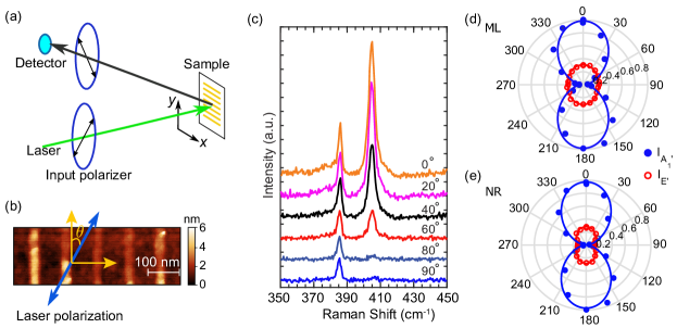
To characterize the structural anisotropy of the ML NRs we utilize polarized Raman spectroscopy, a technique commonly used to probe fundamental phonon modes Lee et al. (2010); Molina-Sanchez and Wirtz (2011) and crystal symmetries. Since Raman spectroscopy is sensitive to structural changes, it is often applied to study layer- and strain-dependent properties of 2D materials Zhang et al. (2015); Saito et al. (2016); Mignuzzi et al. (2015); Conley et al. (2013) and to study nanostructures such as nanocrystals Faraci et al. (2006, 2009); Swamy et al. (2005), graphene chiral edge states You et al. (2008), and graphene and MoS2 NRs Ryu et al. (2011); Bischoff et al. (2011); Wu et al. (2016b). With polarized Raman spectroscopy, the intensity of scattered light is measured as a function of its incident polarization angle.
ML MoS2 has two active Raman modes, and , as a result of its D3h crystal symmetry Saito et al. (2016); Zhang et al. (2015). The mode corresponds to the in-plane vibration of the two sulphur layers of a ML MoS2 and the mode to the out-of-plane vibration of the two sulphur layers. They have different polarization-dependent behaviors in the backscattering measurement scheme illustrated in Fig. 1(a). The mode has two components with polarization parallel and perpendicular to the incident laser polarization respectively, while the mode only has a component with polarization parallel to the incident Saito et al. (2016); Zhang et al. (2015). By comparing the polarization dependence of the intensity of these two modes between ML MoS2 NRs and unpatterned MLs, the effects of anisotropic lateral confinement in NRs may be measured.
Figure 1(b-c) shows polarization resolved Raman spectra for ML MoS2 NRs with a measured ribbon width of about 25 nm, as shown by the AFM image in Fig. 1(b). The analyzer polarization direction is parallel to the ribbons ( direction), and the angle for the incident light polarization is defined as in Fig. 1(b). Figure 1(c) shows the NR Raman spectra with from 0 to 90. Angle-dependence for both Raman modes is evident. Figure 1(d, e) show polar plots of the integrated intensities of Raman modes for ML and NRs. Due to the crystal symmetry in ML MoS2, the mode is almost angle independent while the mode is -dependent. In contrast to unpatterned ML MoS2, the mode in the NRs shows stronger polarization dependence. The intensities for both modes reach maximum (minimum) when incident laser polarization is parallel (perpendicular) to the ribbons. The Raman anisotropy is a clear indication of the symmetry breaking in the ribbon nanostructures. Similar anisotropic Raman spectra are also reported in Ref. (21) for monolayer MoS2 created by helium ion milling, however, the maximum (minimum) for both modes are at 90 (0°) instead of 0°. Our results are confirmed with two different Raman setups and are consistent with other literature Saito et al. (2016); Shi et al. (2016).
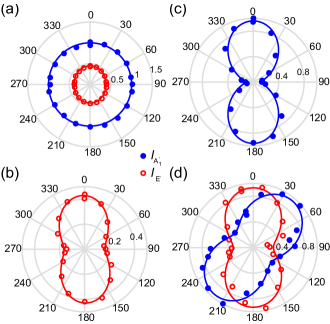
To further elucidate the anisotropy, Raman spectra are collected without the analyzer. Figure 2(a) shows the Raman spectra of ML MoS2; the intensities and are nearly isotropic as expected. In contrast, the and for NRs as shown in Fig. 2(b, c) show strong polarization dependence, clearly revealing the anisotropic Raman behavior. More interestingly, when the analyzer is perpendicular to the NRs, the mode is polarized around , as shown in Fig. 2(d). This indicates that the mode is no longer polarized along with the excitation laser but has other components, clearly been modified by the NR structure. The measurement with various polarization configurations revealed the anisotropic Raman spectra in the ML NRs.
III Size-dependence of Raman Spectra
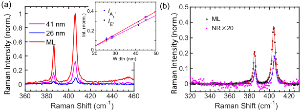
Figure 3(a) shows the Raman spectra for NRs with different ribbon widths. The Raman intensity decreases as the ribbon becomes narrower for both modes, as expected. The integrated Raman intensities of the two modes both follow linear relations to the ribbon width as shown by the insert in Fig. 3(a). Similar linear relations have been observed in graphene and ML MoS2 NRs Bischoff et al. (2011); Wu et al. (2016b). The zero intercept at finite ribbon width ( 10 nm) is an indication that the effective ribbon width is narrower than the measured width, perhaps due to over etching Ryu et al. (2011); Wei et al. (2017).
In graphene NRs and TMD ribbons prepared with other processes, defect modes and linewidth broadening are observed Ryu et al. (2011); Wu et al. (2016b). The Raman spectra of NRs measured here, however, exhibit similar lineshape to an unpatterned ML even in the narrowest NRs measured (Fig. 3(b)). Our calculation (see supplementary materials for details) shows that linewidth broadening for Raman modes in monolayer MoS2 NRs are within 1 cm-1 for ribbons wider than 5 nm, which is beyond the resolution of a typical Raman system. In addition, no Raman modes on the low frequency side are present, indicating that the nanolithography process does not create appreciable structural damage to the ribbons and no edge modes have become measurable. This suggests that our approach represents a nondestructive fabrication process to the patterned ML optical properties, in contrast to recent ion milling approaches Wu et al. (2016b). This conclusion is supported by electrical transport measurements showing comparable mobility in NRs of 40 nm width to that of a ML, except for edge effects which manifest in temperature-dependent mobility measurement (See supplementary materials for details).
IV Photoluminescence Spectroscopy of MoS2 Nanoribbons
In nanomaterials and nanostructures, electron and hole wavefunctions are confined to small scales, resulting in a modification to their energy. Size-tunable optical bandgaps have been observed in graphene NRs due to the confinement effect Han et al. (2007), and recently in ML MoS2 Gopalakrishnan et al. (2015); Gan et al. (2015); Jin et al. (2016); Wei et al. (2017). Similar confinement effects are expected in MoS2 NRs, but they have not yet been reported Wu et al. (2016b); Poh et al. (2017). Our nondestructive fabrication process allows the study of PL from laterally-confined ML MoS2 NRs.
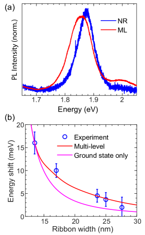
Figure 4(a) shows the PL spectra of an unpatterned ML and NRs fabricated with the same flake. The NRs are measured with a nominal ribbon width of 14 nm. A clear blue-shifted PL peak is present, indicating the confinement effect due to the nanometer-scale lateral width. The spectral linewidth of NRs is slightly narrower (up to 10 meV narrowing), similar to the narrowing observed in ML MoS2 nanodots Wei et al. (2017). This is possibly due to reduced phonon scattering in the confined system. Exfoliated ML MoS2 generally exhibits -doped properties with trion emission in PL Mak et al. (2013); Zhang et al. (2014), and defects along the edges should be considered as possible origins of the energy shift. However, defect induced trion emission in NRs can be excluded since trions possess lower energies than excitons, in contrast to the blue shifting observed here. Furthermore, the energy shift is size-dependent as shown in Fig. 4 (b). The clear trend of larger shift in narrower ribbons suggests a confinement effect.
Since the Bohr radius of excitons in ML MoS2 (and similar TMDs) is extremely small ( nm Ramasubramaniam (2012); Cheiwchanchamnangij and Lambrecht (2012)), one can treat the excitons as quasiparticles whose center-of-mass (CM) motion is quantized in an infinite-deep potential well (Fig. S4). This simple model gives the shift for the ground state as a function of ribbon width as
| (1) |
where is the exciton total mass and is the effective ribbon width (Fig. S4(a)). Similar to that observed in graphene NRs Han et al. (2007) and nanoflake quantum dots of MoS2 MLs Wei et al. (2017), the effective ribbon width is typically several nanometers narrower than that measured with AFM (or scanning electron microscopy) due to the finite AFM tip size and over etching, and the reconfigurable etched edges can also contribute to an narrower effective ribbon width through chemical reactions with water and oxygen in air Han et al. (2007); Ryu et al. (2011). The experimental data is thus fit with , where is the AFM measured nominal ribbon width. The fitting with the phenomenological Eq. 1 gives and nm, where is the free electron mass. The fitted is smaller than the theoretical values which are around , however, the simple model captures the trend of the confinement energy. These size-dependent optical results in nanoribbons are very similar qualitatively to those reported for MoS2 nanodots Wei et al. (2017).
In the weak confinement regime, the narrow energy level spacing and extremely short exciton lifetime in MoS2 complicates emission dynamics from optically-excited excitons. Upon photo-excitation, hot excitons typically undergo a thermalization process through exciton-phonon and exciton-exciton interaction before recombination. However, due to the short radiative lifetime of the tightly bound excitons in ML TMDs (here MoS2) and the reduced scattering rate with phonons in confined systems, excitons can recombine before reaching thermal equilibrium Robert et al. (2016). It is thus reasonable to consider the emissions from higher energy states since the exciton wavefunctions do not spatially redistribute. A similar phenomenon was also reported in conventional semiconductor systems in the weak confinement regime where high energy states occupation are suggested Lee et al. (2011).
To test this idea, a simple model accounting for the first three levels gives fitting parameters of nm and . Figure 4(b) compares this to the typical ground state. The non-equilibrium multilevel model gives very close to the value of around reported in the literature Cheiwchanchamnangij and Lambrecht (2012); Ramasubramaniam (2012). The effective 8 nm width reduction of is comparable to the value observed for graphene NRs prepared with similar lithographically process Ryu et al. (2011). It is also consistent with the 10 nm intercept from size-dependent Raman intensities in the inset in Fig. 3(a). The non-equilibrium multilevel model for emission gives reasonable parameters compared to experiments for size-dependent features. We emphasize that this model is a simple approach to account for the size-dependence expected for fast recombining excitons in the weak confinement regime. A full dynamical model for the NR emission is beyond the scope of these experiments and analysis. Achieving strong lateral confinement with significant energy level separation and increased importance of edge states would lead to distinct PL behavior that has not yet been observed in ML TMD NRs.
V Conclusion
We have shown that high resolution e-beam lithography can be used to pattern ML TMD nanoribbons with deterministic control of lateral size. The NRs prepared by e-beam lithography with positive resist do not show the large defect contributions to optical spectroscopy that appear in NRs prepared by ion milling. The isotropic Raman spectra in ML become anisotropic in NRs and the PL of the nanometer-scale ribbons shows confinement effects that can be modeled assuming a non-equilibrium system. The e-beam lithography approach offers a potential route for fabricating TMD NRs with exotic electrical and magnetic properties, particularly at the edges, that maintain good opto-electronic properties.
Acknowledgements
This work is primarily supported by the Office of Naval research (N00014-16-1-3055) and the Institute for Sustainability and Energy at Northwestern. Characterization and device fabrication made use of the EPIC and SPID facilities of the NUANCE Center at Northwestern University and the Northwestern University Micro/ Nano Fabrication Facility (NUFAB), which have received support from the Soft and Hybrid Nanotechnology Experimental (SHyNE) Resource (NSF NNCI-1542205); the MRSEC program (NSF DMR-1121262) at the Materials Research Center; the International Institute for Nanotechnology (IIN); the Keck Foundation; and the State of Illinois. Use of the Center for Nanoscale Materials was supported by the US Department of Energy, Office of Science, Office of Basic Energy Sciences, under Contract No. DE-AC02-06CH11357. N.P.S. gratefully acknowledges support as an Alfred P. Sloan Research Fellow.
Supplementary Information
Fabrication, size characterization, and modeling details are in the Supplementary Information file.
References
- Xiao et al. (2012) D. Xiao, G.-B. Liu, W. Feng, X. Xu, and W. Yao, “Coupled spin and valley physics in monolayers of MoS2 and other group-VI dichalcogenides,” Phys. Rev. Lett. 108, 196802 (2012).
- Xu et al. (2014) X. Xu, W. Yao, D. Xiao, and T. F. Heinz, “Spin and pseudospins in layered transition metal dichalcogenides,” Nature Phys. 10, 343 (2014).
- Trauzettel et al. (2007) B. Trauzettel, D. V. Bulaev, D. Loss, and G. Burkard, “Spin qubits in graphene quantum dots,” Nature Phys. 3, 192 (2007).
- Libisch et al. (2009) F. Libisch, C. Stampfer, and J. Burgdörfer, “Graphene quantum dots: Beyond a Dirac billiard,” Phys. Rev. B 79, 115423 (2009).
- Han et al. (2007) M. Y. Han, B. Özyilmaz, Y. Zhang, and P. Kim, “Energy band-gap engineering of graphene nanoribbons,” Phys. Rev. Lett. 98, 206805 (2007).
- Brey and Fertig (2006) L. Brey and H. Fertig, “Electronic states of graphene nanoribbons studied with the Dirac equation,” Phys. Rev. B 73, 235411 (2006).
- Dutta and Pati (2010) S. Dutta and S. K. Pati, “Novel properties of graphene nanoribbons: a review,” J. Mater. Chem. 20, 8207 (2010).
- Pan and Zhang (2012) H. Pan and Y.-W. Zhang, “Edge-dependent structural, electronic and magnetic properties of MoS2 nanoribbons,” J. Mater. Chem. 22, 7280 (2012).
- Li et al. (2008) Y. Li, Z. Zhou, S. Zhang, and Z. Chen, “MoS2 nanoribbons: high stability and unusual electronic and magnetic properties,” J. Am. Chem. Soc. 130, 16739 (2008).
- Ataca et al. (2011) C. Ataca, H. Sahin, E. Akturk, and S. Ciraci, “Mechanical and electronic properties of MoS2 nanoribbons and their defects,” J. Phys. Chem. C 115, 3934 (2011).
- Dolui et al. (2012) K. Dolui, C. D. Pemmaraju, and S. Sanvito, “Electric field effects on armchair MoS2 nanoribbons,” ACS Nano 6, 4823 (2012).
- Klinovaja and Loss (2013) J. Klinovaja and D. Loss, “Spintronics in MoS2 monolayer quantum wires,” Phys. Rev. B 88, 075404 (2013).
- Mourik et al. (2012) V. Mourik, K. Zuo, S. M. Frolov, S. Plissard, E. Bakkers, and L. P. Kouwenhoven, “Signatures of Majorana fermions in hybrid superconductor-semiconductor nanowire devices,” Science 336, 1003 (2012).
- Wu et al. (2016a) D. Wu, X. Li, L. Luan, X. Wu, W. Li, M. N. Yogeesh, R. Ghosh, Z. Chu, D. Akinwande, Q. Niu, and K. Lai, “Uncovering edge states and electrical inhomogeneity in MoS2 field-effect transistors,” Proceedings of the National Academy of Sciences 113, 8583 (2016a).
- Jia et al. (2017a) Y. Jia, T. K. Stanev, E. J. Lenferink, and N. P. Stern, “Enhanced conductivity along lateral homojunction interfaces of atomically thin semiconductors,” 2D Materials 4, 021012 (2017a).
- Fei et al. (2017) Z. Fei, T. Palomaki, S. Wu, W. Zhao, X. Cai, B. Sun, P. Nguyen, J. Finney, X. Xu, and D. H. Cobden, “Edge conduction in monolayer WTe2,” Nature Phys. (2017).
- Jia et al. (2017b) Z.-Y. Jia, Y.-H. Song, X.-B. Li, K. Ran, P. Lu, H.-J. Zheng, X.-Y. Zhu, Z.-Q. Shi, J. Sun, J. Wen, D. Xing, and S.-C. Li, “Direct visualization of a two-dimensional topological insulator in the single-layer ,” Phys. Rev. B 96, 041108 (2017b).
- Tang et al. (2017) S. Tang, C. Zhang, D. Wong, Z. Pedramrazi, H.-Z. Tsai, C. Jia, B. Moritz, M. Claassen, H. Ryu, S. Kahn, J. Jiang, H. Yan, M. Hashimoto, D. Lu, R. G. Moore, C.-C. Hwang, C. Hwang, Z. Hussain, Y. Chen, M. M. Ugeda, Z. Liu, T. P. Xie, Xiaoming andDevereaux, M. F. Crommie, S.-K. Mo, and Z.-X. Shen, “Quantum spin Hall state in monolayer 1T’-WTe2,” Nature Phys. 13, 683 (2017).
- Poh et al. (2017) S. M. Poh, S. J. Tan, X. Zhao, Z. Chen, I. Abdelwahab, D. Fu, H. Xu, Y. Bao, W. Zhou, and K. P. Loh, “Large Area Synthesis of 1D-MoSe2 Using Molecular Beam Epitaxy,” Adv. Mater. 29 (2017).
- Liu et al. (2011) Z. Liu, K. Suenaga, Z. Wang, Z. Shi, E. Okunishi, and S. Iijima, “Identification of active atomic defects in a monolayered tungsten disulphide nanoribbon,” Nat. Commun. 2, 213 (2011).
- Wu et al. (2016b) J.-B. Wu, H. Zhao, Y. Li, D. Ohlberg, W. Shi, W. Wu, H. Wang, and P.-H. Tan, “Monolayer molybdenum disulfide nanoribbons with high optical anisotropy,” Adv. Opt. Mater. 4, 756 (2016b).
- Shi et al. (2016) W. Shi, M.-L. Lin, Q.-H. Tan, X.-F. Qiao, J. Zhang, and P.-H. Tan, “Raman and photoluminescence spectra of two-dimensional nanocrystallites of monolayer WS2 and WSe2,” 2D Materials 3, 025016 (2016).
- Wei et al. (2017) G. Wei, D. A. Czaplewski, E. J. Lenferink, T. K. Stanev, I. W. Jung, and N. P. Stern, “Size-tunable Lateral Confinement in Monolayer Semiconductors,” Scientific Reports 7, 3324 (2017).
- Lee et al. (2010) C. Lee, H. Yan, L. E. Brus, T. F. Heinz, J. Hone, and S. Ryu, “Anomalous lattice vibrations of single-and few-layer MoS2,” ACS Nano 4, 2695 (2010).
- Molina-Sanchez and Wirtz (2011) A. Molina-Sanchez and L. Wirtz, “Phonons in single-layer and few-layer MoS2 and WS2,” Phys. Rev. B 84, 155413 (2011).
- Zhang et al. (2015) X. Zhang, X.-F. Qiao, W. Shi, J.-B. Wu, D.-S. Jiang, and P.-H. Tan, “Phonon and Raman scattering of two-dimensional transition metal dichalcogenides from monolayer, multilayer to bulk material,” Chem. Soc. Rev. 44, 2757 (2015).
- Saito et al. (2016) R. Saito, Y. Tatsumi, S. Huang, X. Ling, and M. Dresselhaus, “Raman spectroscopy of transition metal dichalcogenides,” J. Phys. Condens. Matter 28, 353002 (2016).
- Mignuzzi et al. (2015) S. Mignuzzi, A. J. Pollard, N. Bonini, B. Brennan, I. S. Gilmore, M. A. Pimenta, D. Richards, and D. Roy, “Effect of disorder on Raman scattering of single-layer MoS2,” Phys. Rev. B 91, 195411 (2015).
- Conley et al. (2013) H. J. Conley, B. Wang, J. I. Ziegler, R. F. Haglund Jr, S. T. Pantelides, and K. I. Bolotin, “Bandgap engineering of strained monolayer and bilayer MoS2,” Nano Lett. 13, 3626 (2013).
- Faraci et al. (2006) G. Faraci, S. Gibilisco, P. Russo, A. R. Pennisi, and S. La Rosa, “Modified Raman confinement model for Si nanocrystals,” Phys. Rev. B 73, 033307 (2006).
- Faraci et al. (2009) G. Faraci, S. Gibilisco, and A. R. Pennisi, “Quantum confinement and thermal effects on the Raman spectra of Si nanocrystals,” Phys. Rev. B 80, 193410 (2009).
- Swamy et al. (2005) V. Swamy, A. Kuznetsov, L. S. Dubrovinsky, R. A. Caruso, D. G. Shchukin, and B. C. Muddle, “Finite-size and pressure effects on the Raman spectrum of nanocrystalline anatase TiO2,” Phys. Rev. B 71, 184302 (2005).
- You et al. (2008) Y. You, Z. Ni, T. Yu, and Z. Shen, “Edge chirality determination of graphene by Raman spectroscopy,” Appl. Phys. Lett. 93, 163112 (2008).
- Ryu et al. (2011) S. Ryu, J. Maultzsch, M. Y. Han, P. Kim, and L. E. Brus, “Raman spectroscopy of lithographically patterned graphene nanoribbons,” ACS Nano 5, 4123 (2011).
- Bischoff et al. (2011) D. Bischoff, J. Güttinger, S. Dröscher, T. Ihn, K. Ensslin, and C. Stampfer, “Raman spectroscopy on etched graphene nanoribbons,” J. Appl. Phys. 109, 073710 (2011).
- Gopalakrishnan et al. (2015) D. Gopalakrishnan, D. Damien, B. Li, H. Gullappalli, V. K. Pillai, P. M. Ajayan, and M. M. Shaijumon, “Electrochemical synthesis of luminescent MoS2 quantum dots,” Chem. Commun. 51, 6293 (2015).
- Gan et al. (2015) Z. X. Gan, L. Z. Liu, H. Y. Wu, Y. L. Hao, Y. Shan, X. L. Wu, and P. K. Chu, “Quantum confinement effects across two-dimensional planes in MoS2 quantum dots,” Appl. Phys. Lett. 106, 233113 (2015).
- Jin et al. (2016) H. Jin, M. Ahn, S. Jeong, J. H. Han, D. Yoo, D. H. Son, and J. Cheon, “Colloidal Single-Layer Quantum Dots with Lateral Confinement Effects on 2D Exciton,” J. Am. Chem. Soc. 138, 13253 (2016).
- Mak et al. (2013) K. F. Mak, K. He, C. Lee, G. H. Lee, J. Hone, T. F. Heinz, and J. Shan, “Tightly bound trions in monolayer MoS2,” Nature Mater. 12, 207 (2013).
- Zhang et al. (2014) C. Zhang, H. Wang, W. Chan, C. Manolatou, and F. Rana, “Absorption of light by excitons and trions in monolayers of metal dichalcogenide MoS2: Experiments and theory,” Phys. Rev. B 89, 205436 (2014).
- Ramasubramaniam (2012) A. Ramasubramaniam, “Large excitonic effects in monolayers of molybdenum and tungsten dichalcogenides,” Phys. Rev. B 86, 115409 (2012).
- Cheiwchanchamnangij and Lambrecht (2012) T. Cheiwchanchamnangij and W. R. L. Lambrecht, “Quasiparticle band structure calculation of monolayer, bilayer, and bulk MoS2,” Phys. Rev. B 85, 205302 (2012).
- Robert et al. (2016) C. Robert, D. Lagarde, F. Cadiz, G. Wang, B. Lassagne, T. Amand, A. Balocchi, P. Renucci, S. Tongay, B. Urbaszek, and X. Marie, “Exciton radiative lifetime in transition metal dichalcogenide monolayers,” Phys. Rev. B 93, 205423 (2016).
- Lee et al. (2011) L. K. Lee, L. Zhang, H. Deng, and P.-C. Ku, “Room-temperature quantum-dot-like luminescence from site-controlled InGaN quantum disks,” Appl. Phys. Lett. 99, 263105 (2011).