Quantum conductance of MoS2 armchair nanoribbons
Abstract
Molybdenum disulfide (MoS2) is layered transition-metal dichalcogenide (TMDC), which in its monolayer form, has the direct bandgap of 1.8 eV. We investigated the effect of width and strain on quantum transport for MoS2 armchair nanoribbons. That indicates MoS2 armchair nanoribbons are a good candidate for transistors even with strain.
I Introduction
In recent decades, one-dimensional (1D) nanostructures have been extensively investigated because of their interesting properties and their mesoscopic physics. Among them, carbon nanostructures are well-studied, theoretically and experimentallyZhou et al. (1994); Rodriguez et al. (1995); Panella et al. (2005); Kaskhedikar and Maier (2009); Smalley et al. (2003); Son et al. (2006); Smalley et al. (2003). On the other hand, carbon-based nanostructures are not suitable for some applications because of their small bandgap.
Fortunately, a good alternative to carbon-based systems is a class of inorganic layered materials which exhibit different properties and also could be synthesized in the form of nanotubes and nanoribbons Yoon et al. (2011); Radisavljevic et al. (2011); Zhang et al. (2015); Radisavljevic and Kis (2013); Li et al. (2012). These systems could use in a large variety of applications of one-dimensional systems. Molybdenum disulfide (MoS2) is layered transition-metal di-calcogonide (TMDC) semiconductor that has attracted considerable interest because of its properties. In its bulk structure, an indirect bandgap of about 1.2 eV is observed, while in monolayer form, the bandgap increases to 1.8 eV Kuc et al. (2011) with a transition to direct bandgap, which makes it useful for some applications in electronics, optoelectronics, and photovoltaic devicesRadisavljevic and Kis (2013).
It has already been shown that monolayer of MoS2 is an ideal material for valleytronics Zeng et al. (2012). This fact is due to the inversion-symmetry breaking together with spin-orbit coupling leads to coupled spin and valley degree of freedoms in a monolayer of MoS2 and other group-VI dichalcogenides. It means that it is possible to control both spin and valley in these 2D materials. It has been shown that Mo and W dichalcogenides can exhibit two thermodynamically stable hexagonal (H) and tetragonal (T) structural phases which provide opportunities for flexible, low power and transparent electronic devices Duerloo et al. (2014). It has been shown that zigzag nanoribbons are metallic and magnetic and armchair nanoribbons are semiconductor and nonmagnetic Qi et al. (2013); Pan and Zhang (2012). The magnetic state of zigzag nanoribbons becomes more stable after passivation by hydrogen Qi et al. (2013). Passivation by different nonmetal atoms has also been investigated for armchair nanoribbons. It turns out that the most stable structure is obtained when Mo and S atoms are passivated by oxygen and hydrogen, respectively.
In this paper, we focus on armchair nanoribbons. We investigated the effect of width and strain on quantum transport for MoS2 armchair nanoribbons. Due to flexibility and the large band gap of MoS2 nanostructures we investigated the effect of strain on the quantum transport of our structuresDuerloo et al. (2014). That indicates MoS2 armchair nanoribbons are the good candidate for transistors even with strain.
II Computational details
The first-principle calculations are performed utilizing the projector augmented wave (PAW) pseudopotentials in the framework of density functional theory (DFT), as implemented in the Quantum-Espresso packageGiannozzi et al. (2009). The exchange-correlation effects are evaluated using the generalized gradient approximation as proposed by Perdew-Bruke-Ernzerhof (PBE-GGA). The Monkhorest-Pack scheme of kpoint sampling is used for integration over the first Brillouin zone. For monolayer and nanoribbons structures, and k-point meshes are used, respectively. The energy and the wave-function cut-offs are set to 400 Ry and 35 Ry, respectively. We set all vacuum at least to 12 Å. The wannierization is obtained by Marzari and Vanderbilt’s method using the WANNIER90 code wan ; Marzari and Vanderbilt (1997); Marzari et al. (2012, 2003); Mostofi et al. (2008). In the case of entangled energy, we used Souza, Marzari, and Vanderbilt approach Souza et al. (2001).
III Results and disscution
Electronic Properties:
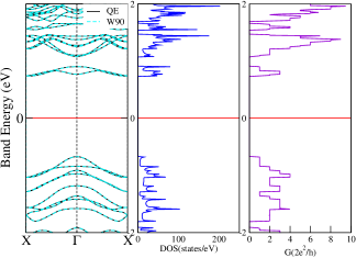
Firstly, we investigated the electronic structure of MoS2 monolayer. The optimized lattice constant was 3.16 Å and the band gap obtained 1.76 eV, in good agreement with the previous calculationKuc et al. (2011). Then we investigated MLWF (Maximally Localized Wannier Function) of the monolayer. We chose d orbital of Mo atom and p orbital of S atoms for initial projections in wannierization and we obtained MLWF for monolayer, in coincident with the previous resultsShi et al. (2013).
After monolayer, we investigated MoS2 nanoribbons. Such as geraphene nanoribbons, MoS2 nanoribbons also can be described with 2 integer indices. So the chiral vector is that causes we have 2 types of nanoribbons: zigzag for and armchair for . From previous calculations, we know that zigzag nanoribbons are metallic and magnetic and armchair nanoribbons are semiconductor and nonmagneticQi et al. (2013). Since our purpose is how to make a transistor, we chose armchair nanoribbons.
After cutting monolayer and building armchair nanoribbons. we optimized lattice constant. Then the electronic spectrum of relaxed structures extracted from band structure calculation (see Fig. 3 and Fig. 4). Others also reported the same results Qi et al. (2013).
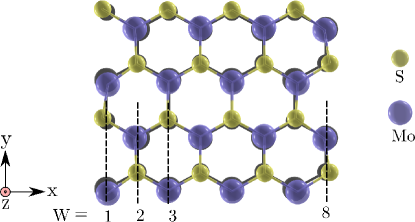
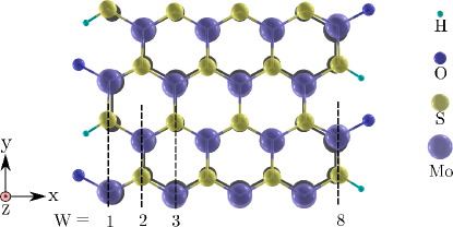
Then we modulated our structures with O and H atoms. Based on Zhang et. al paper Zhang et al. (2015), if each edge S atom is saturated by one H atom and each edge Mo atom is saturated by one O atom. As shown in (Fig.1) and (Fig.2) in the case of ANR-bare the edge atoms after relaxation are more displaced than the case of ANR-passivated so passivation cause order in structure. We can see the bandgap of AMoS2NR-H-Os converges to 1.4 eV that closer to the bandgap of monolayer compare to bare-nanoribbons (Fig. 2), and then similarity to bare-nanoribbons we obtained band structure of passivated nanoribbons.
Then binding energy per atom has been defined as:
| (1) |
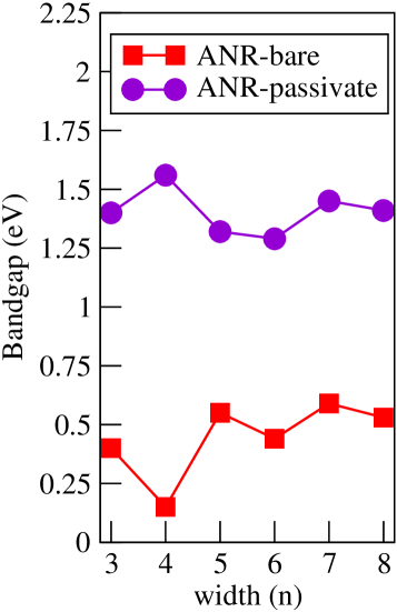
and computed for each width. In table (1) you can see bond length for edge atom and binding energies for every width. You can see our results for 3-AMoS2NR to 8-AMoS2NR (see Fig. 4). Our result is in good agreement with the previous result Zhang et al. (2015). The bandgap is oscillating like the previous study but there is an interesting point in 4-ANR.
| W | dMo-O Å | dS-H Å | dS-Mo Å | Eb(eV) | Eg(bare)(eV) | Eg(passivated)(eV) |
| 3 | 1.70 | 1.36 | 2.56 | -3.99 | 0.40 | 1.40 |
| 4 | 1.70 | 1.35 | 2.37 | -4.11 | 0.15 | 1.56 |
| 5 | 1.71 | 1.36 | 2.56 | -4.10 | 0.55 | 1.32 |
| 6 | 1.71 | 1.36 | 2.37 | -4.11 | 0.44 | 1.29 |
| 7 | 1.71 | 1.36 | 2.56 | -4.10 | 0.59 | 1.45 |
| 8 | 1.71 | 2.57 | 2.37 | -4.10 | 0.53 | 1.41 |
For optimization lattice constant of nanoribbons we should obtain the relation between total energy and lattice constant. Because our structure is periodic in the y-direction we plotted total energy in terms of lattice constant in the y-direction. For all structure, we get one minimum in the plot but for 4-AMoS2NR-bare we got two minima. Of course, the global minima was right and was in good agreement with other works Fan et al. (2014). But there was another minimum that should be investigated (Fig. 8). As you saw in Fig. 4, the graph of an increasing/decreasing of bandgap after passivation remains as the same in bare one except for 4-AMoS2NR. We investigate this little subject in the app. A.
MLWF and quantum transport:
After that, we should obtain MLWF for each nanoribbon. It should be noted that choosing some appropriate begin projections for wannierization lead to meaningful localized orbitals. After obtaining MLWF of each nanoribbon we can investigate the quantum transport of our systems. You can see our results in Fig. 4, as you see with increasing width of the AMoS2NR-H-Os number of passing channel is increased and the value of G (the quantum transport for each energy) is increased too.
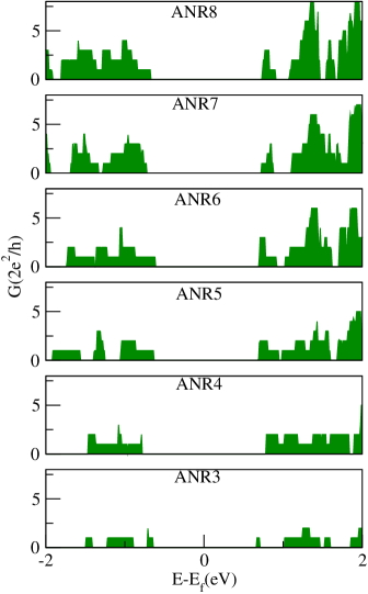
It should be noted that only electrons at the (Fermi energy) playing a role in the quantum conductance. At finite temperature, every sub-band near the can contribute to the quantum conductance. The current, for a finite bias voltage (V), is given by Bagwell and Orlando (1989)
| (2) | ||||
where f is the Fermi-Dirac distribution function and is the chemical potential. At a finite temperature has a Gaussian peak that at K becomes a Dirac delta function. We can estimate that at room temperature the current can be approximated by integrating over eV Rasuli et al. (2010) and compute conductance room temperature.
Because of bandgap presence in AMoS2NR-H-O, we can use them in transistors. As a result, we should check how the quantum transport change if the system influence by various gate voltage (see Fig. 7 a) As you see all of the nanoribbons are good for transistors because of their high ratio of On/Off in different gate voltages. But one should choose a proper gate voltage for transistors. For example, if you want to use 8-AMoS2NR-H-O for the transistor using 0.8 V and 1.1 V to 1.5 V value for gate voltage is recommended.
Response of AMoS2NR-H-Os to strain:
We investigated the effect of strain on AMoS2NR-H-O. According to previous worksPan and Zhang (2012) we know that there are two typical families of AMoS2NR-H-O, symmetric for odd width and asymmetric for even width. As a result, AMoS2NR-H-O with widths w = 7 and 8 was chosen to represent two typical families of AMoS2NR-H-O. Now we want to extract band structure in various strain and you can see our result in fig(5), with both positive and negative strain bandgap is decreased for both symmetric and asymmetric nanoribbons. With increasing or decreasing strain the number of passing channel for electrons is increased.
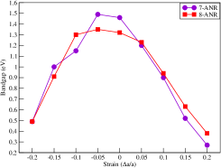
Figure 6 shows the quantum transport of the 7-,8-AMoS2NR-H-O under various induced strain at T = 0 K.
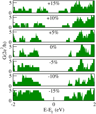
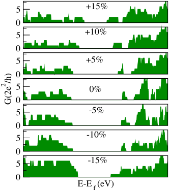
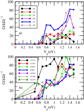
In room temperature, we can use Eq. 2 for computing quantum conductance in various strain for the 7-,8-AMoS2NR-H-O as you see in Fig. 7. With increasing or decreasing strain the number of passing channel for electrons is increased, but as you see in Fig. 7 in room temperature 7-,8-AMoS2NR-H-O have low conductance, as a result, you can use them for the transistor in high strain. Also if there is for example 1 V gate voltage you can use these nanoribbons as strain sensors.
IV Conclusion
Density functional studies of nanoribbons width and strain effects on the electrical transport properties of the AMoS2NR-H-O are presented. By applying a uniaxial tensile strain in the y-direction, the electronic properties of the AMoS2NR-H-O nanoribbons were studied. Using the Wannier functions, the band structure and density of states were calculated for different strains from -15% to +15%. It is observed that AMoS2NR-H-O in different width and different strain are a good candidate for using in the transistor. In addition, you can use them for strain sensors.
Acknowledgements.
We would like to acknowledge the Isfahan University of Technology. The authors gratefully acknowledge the Sheikh Bahaei National High Performance Computing Center (SBNHPCC) for providing computing facilities and time. SBNHPCC is supported by scientific and technological department of presidential office and Isfahan University of Technology (IUT). Discussions with …about various choices of methods are appreciated.Appendix A ANR-4-bare
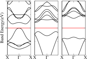
We guessed that maybe there is a bond that reinforced in the second minimum in compare with maximum, so we checked that and we saw that (Fig. 8). But there was no bond that approves this guess. Then we investigate that if one of this minimum or maximum has magnetic structure, and the value of total magnetization is zero. We plot band structure for these 3 that you can see in Figs.(9).
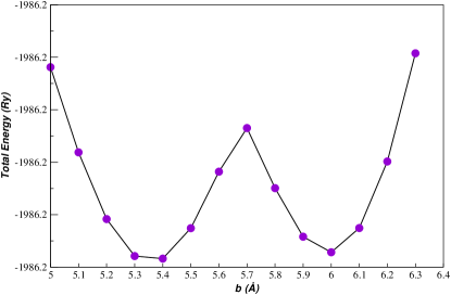
We have seen that in the case of 4-AMoS2NR-bare for lattice parameter 5.4 the bandgap is 0.15 eV (indirect) that is in good agreement with the previous result, and in the case of 4-AMoS2NR-bare for lattice parameter 5.7,6.0 the band gap is 0.32eV (indirect) and 0.67eV (direct in point) respectively.
References
- Zhou et al. (1994) O. Zhou, R. Fleming, D. Murphy, C. Chen, R. Haddon, A. Ramirez, and S. Glarum, Science 263, 1744 (1994).
- Rodriguez et al. (1995) N. M. Rodriguez, A. Chambers, and R. T. K. Baker, Langmuir 11, 3862 (1995).
- Panella et al. (2005) B. Panella, M. Hirscher, and S. Roth, Carbon 43, 2209 (2005).
- Kaskhedikar and Maier (2009) N. A. Kaskhedikar and J. Maier, Advanced Materials 21, 2664 (2009).
- Smalley et al. (2003) R. E. Smalley, M. S. Dresselhaus, G. Dresselhaus, and P. Avouris, Carbon nanotubes: synthesis, structure, properties, and applications, Vol. 80 (Springer Science & Business Media, 2003).
- Son et al. (2006) Y.-W. Son, M. L. Cohen, and S. G. Louie, Physical review letters 97, 216803 (2006).
- Yoon et al. (2011) Y. Yoon, K. Ganapathi, and S. Salahuddin, Nano letters 11, 3768 (2011).
- Radisavljevic et al. (2011) B. Radisavljevic, A. Radenovic, J. Brivio, i. V. Giacometti, and A. Kis, Nature nanotechnology 6, 147 (2011).
- Zhang et al. (2015) L. Zhang, L. Wan, Y. Yu, B. Wang, F. Xu, Y. Wei, and Y. Zhao, The Journal of Physical Chemistry C 119, 22164 (2015).
- Radisavljevic and Kis (2013) B. Radisavljevic and A. Kis, Nature Materials 12, 815 (2013).
- Li et al. (2012) Y. Li, D. Wu, Z. Zhou, C. R. Cabrera, and Z. Chen, The journal of physical chemistry letters 3, 2221 (2012).
- Kuc et al. (2011) A. Kuc, N. Zibouche, and T. Heine, 245213, 1 (2011).
- Zeng et al. (2012) H. Zeng, J. Dai, W. Yao, D. Xiao, and X. Cui, Nature Nanotechnology , 1 (2012).
- Duerloo et al. (2014) K.-A. N. Duerloo, Y. Li, and E. J. Reed, Nature communications 5 (2014).
- Qi et al. (2013) Z. Qi, P. Cao, and H. S. Park, Journal of Applied Physics 114, 1 (2013).
- Pan and Zhang (2012) H. Pan and Y.-W. Zhang, Journal of Materials Chemistry 22, 7280 (2012).
- Giannozzi et al. (2009) P. Giannozzi, S. Baroni, N. Bonini, M. Calandra, R. Car, C. Cavazzoni, D. Ceresoli, G. L. Chiarotti, M. Cococcioni, I. Dabo, et al., Journal of physics: Condensed matter 21, 395502 (2009).
- (18) “wannier90,” .
- Marzari and Vanderbilt (1997) N. Marzari and D. Vanderbilt, Physical Review B 56, 12847 (1997).
- Marzari et al. (2012) N. Marzari, A. a. Mostofi, J. R. Yates, I. Souza, and D. Vanderbilt, Reviews of Modern Physics 84, 1419 (2012).
- Marzari et al. (2003) N. Marzari, I. Souza, and D. Vanderbilt, Psi-K newsletter , 129 (2003).
- Mostofi et al. (2008) A. A. Mostofi, J. R. Yates, Y.-S. Lee, I. Souza, D. Vanderbilt, and N. Marzari, Computer Physics Communications 178, 685 (2008), arXiv:0708.0650 .
- Souza et al. (2001) I. Souza, N. Marzari, and D. Vanderbilt, Physical Review B 65, 035109 (2001).
- Shi et al. (2013) H. Shi, H. Pan, Y.-W. Zhang, and B. I. Yakobson, Physical Review B 87, 155304 (2013).
- Fan et al. (2014) D. D. Fan, H. J. Liu, L. Cheng, P. H. Jiang, J. Shi, X. F. Tang, D. D. Fan, H. J. Liu, L. Cheng, P. H. Jiang, J. Shi, and X. F. Tang, 133113, 3 (2014).
- Bagwell and Orlando (1989) P. F. Bagwell and T. P. Orlando, Phys. Rev. B 40, 1456 (1989).
- Rasuli et al. (2010) R. Rasuli, H. Rafii-Tabar, and A. I. zad, Phys. Rev. B 81, 125409 (2010).