Two-dimensional InSe as a potential thermoelectric material
Abstract
Thermoelectric properties of monolayer indium selenide (InSe) are investigated by using Boltzman transport theory and first-principles calculations as a function of Fermi energy and crystal orientation. We find that the maximum power factor of p-type (n-type) monolayer InSe can be as large as 0.049 (0.043) W/K2m at 300 K in the armchair direction. The excellent thermoelectric performance of monolayer InSe is attributed to both of its Seebeck coefficient and electrical conductivity. The large Seebeck coefficient originates from the moderate (about 2 eV) band gap of monolayer InSe as an indirect gap semiconductor, while its large electrical conductivity is due to its unique two-dimensional density of states (DOS), which consists of an almost constant DOS near the conduction band bottom and a sharp peak near the valence band top.
Recent advances in the fabrication and characterization of two-dimensional (2D) materials such as the transition metal dichalcogenides (TMDs), black phosphorus (BP), and group III chalcogenides have allowed researchers to look up unique electronic properties of the materials and utilize them in various electronic applications. Wang et al. (2012); Butler et al. (2013); Geim and Grigorieva (2013) Research on thermoelectricity, which is intended to convert waste heat into electric energy, should also benefit from the advances of the 2D materials. Unlike graphene, the TMDs, BP, and group III chalcogenides have sizable band gaps that could enable the enhancement of thermoelectric properties due to the quantum confinement effects in the low-dimensional semiconductors. Dresselhaus et al. (2007); Hung et al. (2016) It is thus important to predict the best thermoelectric 2D material theoretically.
A good thermoelectric material is characterized by how efficient electricity can be obtained for a given heat source, in which two quantities are often used for evaluation: (1) power factor, , where is the Seebeck coefficient and is the electrical conductivity; and (2) figure of merit , where is the thermal conductivity and is the average absolute temperature. The PF specifies how much electricity can be generated, while specifies how efficient electricity is obtained for a given temperature difference. The improvement of thermoelectric devices thus strongly depends on the optimization of electronic and thermal transport properties, in which the 2D materials may serve as a good candidate. Saito et al. (2016); Fei et al. (2014); Liao et al. (2015); Yoshida et al. (2016); Kayyalha et al. (2016) For example, using the electric-double-layer transistor configuration, it was found that the Seebeck coefficient of 2D BP reached 510 at 210 , which is much higher than the bulk BP (340 at 300 ). Saito et al. (2016) Monolayer BP also exhibits a strong spatial anisotropy in electrical and thermal conductivities, which makes the in the armchair direction larger than that in the zigzag direction. Fei et al. (2014); Liao et al. (2015) However, it is known that the 2D BP reacts strongly with chemical species in air and thus the thermoelectric device can be quickly degrading. As for TMDs such as MoS2, MoSe2, WS2 and WSe2, these materials show thickness-dependent thermoelectric properties and maximum PF of about 0.34 and 0.15 for n-type monolayer MoSe2 and p-type MoS2 monolayers, respectively, which are much higher than those of bulk (0.02 and 0.03 for bulk n-type MoSe2 and p-type MoS2, respectively). Wickramaratne et al. (2014)
In the family of 2D semiconductors, the band structure of monolayer group III chalcogenides such as InSe, GaSe, or GaS are rather unusual, having combination of a flat band at the top of the valence band and a parabolic band at the bottom of conduction band. This feature leads to appearance of a very sharp peak in the electronic density of states (DOS) at the top of the valence band and an almost constant DOS at the bottom of the conduction band. Zólyomi et al. (2013, 2014) A recent report by Geim’s group has shown that the carrier mobility in few-layer InSe may exceed 103 at room temperature. Bandurin et al. (2016) In an earlier experiment, Rhyee et al. showed that the bulk InSe crystal exhibits a low thermal conductivity, W/mK, at room temperature, Rhyee et al. (2009) and the thermal conductivity decreases with increasing temperature ( W/mK at 705 K), giving . By using constant relaxation time in Boltzmann transport theory, Wickramaratne et al., Wickramaratne et al. (2015) showed thickness-dependent thermoelectric properties of 2D group III chalcogenides. From these results, it seems that both the electrical and thermal transport properties of InSe are beneficial for thermoelectric performance and efficiency with both high PF and . We thus expect that InSe in its 2D form could be a good thermoelectric material.
In this work, we evaluate the thermoelectric properties of monolayer InSe by Boltzmann transport theory and first-principles calculations, with a particular focus on its PF. To calculate the constituents of PF, i.e., and , we need the electronic energy dispersion and the carrier relaxation time for each band and for each wave vector k. The electronic structure and relaxation time calculations are possible to perform from first-principles by using Quantum ESPRESSO Giannozzi et al. (2009) and electron-phonon Wannier (EPW) Giustino et al. (2007); Poncé et al. (2016) packages, respectively. The ground-state electronic structure is calculated within the norm-conserving pseudopotential with the Perdew-Zunger Perdew and Zunger (1981) local density approximation (LDA) pse for the exchange-correlation functional and a plane-wave basis set with kinetic energy cutoff of 160 Ry. Note that the LDA without spin-orbit interaction is adopted in this work because the band gap is not really affected by the spin-orbit interaction. Debbichi et al. (2015) The system is modeled by adopting a hexagonal supercell geometry where the vacuum distance is set to 12 Å to eliminate the interactions between the InSe layer and focus on the monolayer in the simulation. To obtain the the optimized geometry, the atomic positions and supercell vectors are fully relaxed by using the Broyden-Fretcher-Goldfarb-Shanno minimization method. Broyden (1970); Fletcher (1970); Goldfarb (1970); Shanno (1970) This system is considered to be optimized when all the Hellmann-Feynman forces and all components of the stress are less than Ry/a.u. and GPa, respectively, which are adequate for the present purpose.
The inputs for the EPW package are the electron energy and phonon dispersions. We compute the electron energy on a k-point grid and the phonon dispersion on a q-point grid. The electron-phonon matrix elements are first computed on these coarse grids, and then interpolated to a dense mesh of both k and q-points of based on the maximally localized Wannier functions in the EPW package because a dense finer grid is necessary to evaluate transport properties. Baroni et al. (2001) The main output of the EPW package is the imaginary part of the electron self-energy calculated from the interpolated ultra-dense electron-phonon matrix elements, which then gives us the relaxation time for each electronic state by the relation , where is the reduced Planck constant. We use Gaussian broadening with a small parameter of 10 meV to approximate the function in . In the calculation of scattering rate, the electron-phonon scattering due to acoustic, optical, and polar optical phonons are all included within the EPW package. Verdi and Giustino (2015); Liu et al. (2017) For simplicity, in the calculation of the relaxation time we do not take into account the so-called “momentum relaxation time”, Lundstrom (2009) which is related to the momentum loss in the scattering processes.
Having the information of the energy band structure and carrier relaxation time, we can calculate the Seebeck coefficient and electrical conductivity along a certain direction (- or -direction) by employing the Boltzmann transport theory within the relaxation time approximation (RTA): Goldsmid (2010); Liao et al. (2015); Li (2015)
| (1) | ||||
| (2) |
where is the unit (positive) electric charge, is the average temperature of the material, is the number of k points, is the volume of the unit cell using a constant thickness of 0.8 nm for the monolayer InSe, Bandurin et al. (2016) is the Fermi energy, is the Fermi-Dirac distribution function, and is the component of the group velocity () in a particular direction at each k point, the factor 2 in Eq. (2) accounts for the spin degeneracy. Li (2015) Note that the RTA can usually be justified for near-equilibrium transport and for specific types of scattering (i.e., elastic, isotropic, or both), while in the case of inelastic scattering (for example, by polar optical phonons which we include in this study) we may have to consider additional approximations. Kaasbjerg et al. (2012) Nevertheless, the relaxation time which includes the polar phonon scattering can still be defined in EPW package from the imaginary part of the electronic self-energy in the inelastic scattering. Kaasbjerg et al. (2012)
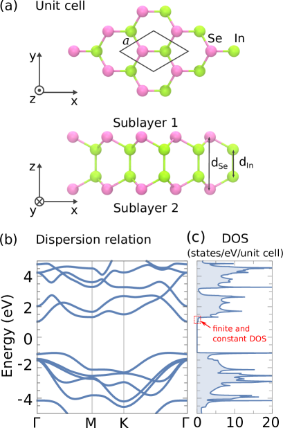
Figure 1(a) shows the top view and side view of the unit cell of monolayer InSe with the lattice constant . Two sublayers exists in a monolayer InSe, in which the first and second sublayers are separated by and from the optimized geometry calculation. In Fig. 1(b), we give the electronic structure of the monolayer InSe from the LDA calculation. The minimum point of the first conduction band appears at the point, while the maximum of the first valence band appears at a point along the - direction. The indirect band gap of monolayer InSe within the LDA is about 2.06 eV. Here is set to be in the center of the energy gap. Since the Seebeck coefficients are sensitive to the choice of the band gap, we also check the band gaps obtained by using the Perdew-Burke-Ernzerhof (PBE) Perdew et al. (1996) and the Heyd-Scuseria-Ernzerhof (HSE) Zólyomi et al. (2014) hybrid functionals, which result in band gaps of about 1.55 eV and 2.24 eV, respectively. The HSE approach is the closest to the band gap of monolayer InSe observed in the experiment. Bandurin et al. (2016) However, the EPW package does not support the HSE pseudopotential. Therefore, the LDA with 2.06 eV band gap is a reasonable approximation in this study. Figure 1(c) shows the DOS of the monolayer InSe, in which we can see a very sharp DOS at the top of the valence band. In the conduction band, a finite and almost constant 2D DOS appears for a limited range within 1.0–1.3 eV. We argue that the existence of such DOS characteristics should be relevant to the excellent thermoelectric of properties of the 2D monolayer InSe that we will discuss below.
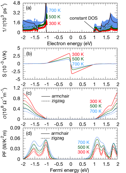
In Figs. 2(a-d), we show the transport and thermoelectric properties of monolayer InSe. Firstly, Fig. 2(a) depicts the scattering rate () for all k states in the electron energy range eV for three different temperatures: 300 K, 500 K, and 700 K at eV. Carrier densities needed to reach eV and eV are cm-3 and cm-3 for hole doping and electron doping, respectively. Since , the shape of the curve resembles that of the DOS. The increase of temperature also enhances the relaxation time . We find a relatively small value of scattering rate at the conduction band of monolayer InSe, leading to a larger relaxation time at energy around 1.0-1.3 eV. We thus expect that the power factor is enhanced in this conducting regime for the n-type InSe. On the other hand, within the valence band, the scattering rate is larger (the relaxation time is smaller) but there is a very sharp DOS at energy around top of the valence band which, according to the Mahan-Sofo theory, Mahan and Sofo (1996) is also a good region to obtain an enhancement of the PF.
In Fig. 2(b), we show the Seebeck coefficient as a function of Fermi energy . The rigid band approximation is adopted to calculate the thermoelectric properties, which assumes that the band structure remains unchanged as we move the Fermi level up and down to simulate the electron and hole doping, respectively. It is a good approximation as long as the doping levels used are not high enough to change the bonding properties of the material. Goldsmid (2010) The larger is found at lower temperature since as given in Eq. (1). The maximum value of for monolayer InSe at room temperature can be more than 3000 , which is also a very large among the 2D materials. This value of is mainly determined by the band gap of the monolayer InSe, in which for band gaps much larger than the thermal energy we can approximate the Seebeck coefficient to be proportional to the band gap. Hung et al. (2015)
The transport coefficients such as and are often measured in a particular direction. In the case of monolayer InSe, we have defined the armchair and zigzag direction from the - and -axes as shown in Fig. 1(a). Therefore, besides the temperature dependence, there is also an orientation dependence of the transport coefficients. However, for the Seebeck coefficient in Fig. 2(b), we find that the values of the two orientations almost overlap to each other. The origin of this behavior can be traced back to the contribution of the group velocity in both the numerator and the denominator parts of Eq. (1), where the contribution from group velocity might be vanished by the division. On the other hand, we show in Fig. 2(c) that the electrical conductivity depends on the crystal orientation because only one group velocity term appears in the expression of in Eq. (2) and the band structure (thus group velocity) of monolayer InSe is slightly anisotropic. We find that the armchair direction of monolayer InSe gives a larger than the zigzag direction. For example, at room temperature and eV (the location of PF maximum in n-type monolayer InSe), we have S/m for the armchair direction, while S/m for the zigzag direction.
By combining and , we can calculate PF as a function of Fermi energy, as shown in Fig. 2(d). The largest PF should be obtained for the armchair direction at the high temperature in both p-type and n-type monolayer InSe (PF value of the p-type monolayer InSe is close to that of the n-type). This result slightly differs with that calculated by Wickramaratne et al., Wickramaratne et al. (2015) which stated that the p-type monolayer InSe has a much larger PF than the n-type. The discrepancy should come from the fact that they treated the relaxation time as a constant, Wickramaratne et al. (2015) while in this work we consider to be energy-dependent as a result of taking the electron-phonon scattering into account. Nevertheless, we note that the PF of p-type monolayer InSe is still on the same order of magnitude with that of the n-type. Therefore, experimentalists could have flexibility to dope monolayer InSe and to obtain the most optimized PF depending on the device setup. From our calculation, the carrier density needed to reach the maximum PF in the p-type (n-type) monolayer InSe is about () cm-3 by hole (electron) doping.
The high PF in monolayer InSe originates from both the large and , corresponding to the unique band structure of monolayer InSe with semiconducting and unusual shape of DOS, respectively. Furthermore, we have shown in a previous work that one way to obtain large PF is by using a low-dimensional semiconductor with high intrinsic carrier mobility and small confinement length (the thickness of the 2D material in this case). Hung et al. (2016) The confinement length of monolayer InSe is found to be very small, about 0.8 nm, compared with thermal de Broglie wavelength nm at room temperature Bandurin et al. (2016) and thus improving the PF of the monolayer InSe compared to its bulk form. Wickramaratne et al., Wickramaratne et al. (2015) reported PF () W/K2m for bulk p-type (n-type) InSe, which is much smaller than that of 2D InSe with PF () W/K2m for monolayer p-type (or n-type) InSe. It should be noted that, not only the dimensionality, but the scattering mechanisms and DOS could also be important to enhance the PF. Kim et al. (2009)
In conclusion, monolayer InSe has been shown to be a potential thermoelectric material with high PF. We expect that a further examination on the thermal conductivity could suggest us the best value of . As a rough estimate, if we use of monolayer InSe of about 27 , Nissimagoudar et al. (2017) combined with PF () W/K2m, it might be possible to achieve of about 0.54 (0.48) for p-type (n-type) InSe at room temperature. Other group III chalcogenides materials such as GaS and GaSe in their 2D forms, having similar band structures with InSe, may also be good candidates for thermoelectric applications.
Acknowledgments
N.T.H. and A.R.T.N are supported by the Interdepartmental Doctoral Degree Program for Multidimensional Materials Science Leaders in Tohoku University. R.S. acknowledges JSPS KAKENHI Grant Numbers JP25107005 and JP25286005.
References
- Wang et al. (2012) Q. Wang, K. Kalantar-Zadeh, A. Kis, J. N. Coleman, and M. S. Strano, Nat. Nanotechnol. 7, 699 (2012).
- Butler et al. (2013) S. Z. Butler, S. M. Hollen, L. Cao, Y. Cui, J. A. Gupta, H. R. Gutiérrez, T. F. Heinz, S. S. Hong, J. Huang, A. F. Ismach, E. Johnston-Halperin, M. Kuno, V. V. Plashnitsa, R. D. Robinson, R. S. Ruoff, S. Salahuddin, J. Shan, L. Shi, M. G. Spencer, M. Terrones, W. Windl, and J. E. Goldberger, ACS Nano 7, 2898 (2013).
- Geim and Grigorieva (2013) A. K. Geim and I. V. Grigorieva, Nature 499, 419 (2013).
- Dresselhaus et al. (2007) M. S. Dresselhaus, G. Chen, M. Y. Tang, R. G. Yang, H. Lee, D. Z. Wang, Z. F. Ren, J. P. Fleurial, and P. Gogna, Adv. Mater. 19, 1043 (2007).
- Hung et al. (2016) N. T. Hung, E. H. Hasdeo, A. R. T. Nugraha, M. S. Dresselhaus, and R. Saito, Phys. Rev. Lett. 117, 036602 (2016).
- Saito et al. (2016) Y. Saito, T. Iizuka, T. Koretsune, R. Arita, S. Shimizu, and Y. Iwasa, Nano Lett. 16, 4819 (2016).
- Fei et al. (2014) R. Fei, A. Faghaninia, R. Soklaski, J. A. Yan, C. Lo, and L. Yang, Nano Lett. 14, 6393 (2014).
- Liao et al. (2015) B. Liao, J. Zhou, B. Qiu, M. S. Dresselhaus, and G. Chen, Phys. Rev. B 91, 235419 (2015).
- Yoshida et al. (2016) M. Yoshida, T. Iizuka, Y. Saito, M. Onga, R. Suzuki, Y. Zhang, Y. Iwasa, and S. Shimizu, Nano Lett. 16, 2061 (2016).
- Kayyalha et al. (2016) M. Kayyalha, J. Maassen, M. Lundstrom, L. Shi, and Y. P. Chen, J. Appl. Phys. 120, 134305 (2016).
- Wickramaratne et al. (2014) D. Wickramaratne, F. Zahid, and R. K. Lake, J. Chem. Phys. 140, 124710 (2014).
- Zólyomi et al. (2013) V. Zólyomi, N. D. Drummond, and V. I. Fal’ko, Phys. Rev. B 87, 195403 (2013).
- Zólyomi et al. (2014) V. Zólyomi, N. D. Drummond, and V. I. Fal’ko, Phys. Rev. B 89, 205416 (2014).
- Bandurin et al. (2016) D. A. Bandurin, A. V. Tyurnina, L. Y. Geliang, A. Mishchenko, V. Zólyomi, S. V. Morozov, R. K. Kumar, R. V. Gorbachev, Z. R. Kudrynskyi, S. Pezzini, Z. D. Kovalyuk, U. Zeitler, K. S. Novoselov, Patané, L. Eaves, I. V. Grigorieva, V. I. Fal’ko, A. K. Geim, and Y. Cao, Nat. Nanotechnol. 12, 223 (2017).
- Rhyee et al. (2009) J. S. Rhyee, K. H. Lee, S. M. Lee, E. Cho, S. I. Kim, E. Lee, Y. S. Kwon, J. H. Shim, and G. Kotliar, Nature 459, 965 (2009).
- Wickramaratne et al. (2015) D. Wickramaratne, F. Zahid, and R. K. Lake, J. Appl. Phys. 118, 075101 (2015).
- Giannozzi et al. (2009) P. Giannozzi, S. Baroni, N. Bonini, M. Calandra, R. Car, C. Cavazzoni, D. Ceresoli, G. L. Chiarotti, M. Cococcioni, I. Dabo, A. D. Corso, S. de Gironcoli, S. Fabris, G. Fratesi, R. Gebauer, U. Gerstmann, C. Gougoussis, A. Kokalj, M. Lazzeri, L. Martin-Samos, N. Marzari, F. Mauri, R. Mazzarello, S. Paolini, A. Pasquarello, L. Paulatto, C. Sbraccia, S. Scandolo, G. Sclauzero, A. P. Seitsonen, A. Smogunov, P. Umari, and R. M. Wentzcovitch, J. Phys. Condens. Matter 21, 395502 (2009).
- Giustino et al. (2007) F. Giustino, M. L. Cohen, and S. G. Louie, Phys. Rev. B 76, 165108 (2007).
- Poncé et al. (2016) S. Poncé, E. Margine, C. Verdi, and F. Giustino, Comput. Phys. Commun. 209, 116 (2016).
- Perdew and Zunger (1981) J. P. Perdew and A. Zunger, Phys. Rev. B 23, 5048 (1981).
- (21) “We used the in.pz-hgh.upf and se.pz-hgh.upf pseudopotentials from http://www.quantum-espresso.org.” .
- Debbichi et al. (2015) L. Debbichi, O. Eriksson, and S. Lebègue, J. Phys. Chem. Lett. 6, 3098 (2015).
- Broyden (1970) C. G. Broyden, IMA J. Appl. Math. 6, 76 (1970).
- Fletcher (1970) R. Fletcher, Comput. J. 13, 317 (1970).
- Goldfarb (1970) D. Goldfarb, Math. Comput. 24, 23 (1970).
- Shanno (1970) D. F. Shanno, Math. Comput. 24, 647 (1970).
- Baroni et al. (2001) S. Baroni, S. de Gironcoli, A. Dal Corso, and P. Giannozzi, Rev. Mod. Phys. 73, 515 (2001).
- Verdi and Giustino (2015) C. Verdi and F. Giustino, Phys. Rev. Lett. 115, 176401 (2015).
- Liu et al. (2017) T.-H. Liu, J. Zhou, B. Liao, D. J. Singh, and G. Chen, Phys. Rev. B 95, 075206 (2017).
- Lundstrom (2009) M. Lundstrom, Fundamentals of carrier transport (Cambridge University Press, New York, 2009).
- Goldsmid (2010) H. J. Goldsmid, Introduction to Thermoelectricity (Springer-Verlag, Berlin Heidelberg, 2010).
- Li (2015) W. Li, Phys. Rev. B 92, 075405 (2015).
- Kaasbjerg et al. (2012) K. Kaasbjerg, K. S. Thygesen, and K. W. Jacobsen, Phys. Rev. B 85, 115317 (2012).
- Perdew et al. (1996) J. P. Perdew, K. Burke, and M. Ernzerhof, Phys. Rev. Lett. 77, 3865 (1996).
- Mahan and Sofo (1996) G. D. Mahan and J. O. Sofo, Proc. Natl. Acad. Sci. U.S.A. 93, 7436 (1996).
- Hung et al. (2015) N. T. Hung, A. R. T. Nugraha, E. H. Hasdeo, M. S. Dresselhaus, and R. Saito, Phys. Rev. B 92, 165426 (2015).
- Kim et al. (2009) R. Kim, S. Datta, and M. S. Lundstrom, J. Appl. Phys. 105, 034506 (2009).
- Nissimagoudar et al. (2017) A. Nissimagoudar, J. Ma, Y. Chen, and W. Li, J. Phys. Condens. Matter 29, 335702 (2017).