∎
11email: yx3ga@virginia.edu
From materials to systems: a multiscale analysis of nanomagnetic switching
Abstract
With the increasing demand for low-power electronics, nanomagnetic devices have emerged as strong potential candidates to complement present day transistor technology. A variety of novel switching effects such as spin torque and giant spin Hall offer scalable ways to manipulate nano-sized magnets. However, the low intrinsic energy cost of switching spins is often compromised by the energy consumed in the overhead circuitry in creating the necessary switching fields. Scaling brings in added concerns such as the ability to distinguish states (readability) and to write information without spontaneous backflips (reliability). A viable device must ultimately navigate a complex multi-dimensional material and design space defined by volume, energy budget, speed and a target read-write-retention error. In this paper, we review the major challenges facing nanomagnetic devices and present a multi-scale computational framework to explore possible innovations at different levels (material, device, or circuit), along with a holistic understanding of their overall energy-delay-reliability tradeoff.
Keywords:
nanomagnetics, STT-MRAM, computational spintronics, spin logic, neuromorphic spintronics.1 Introduction
Power dissipation is a major concern in fast growing mobile applications where computations must be performed with a limited power budget. One of the fundamental issues with electronic devices is their need to move several electrons to charge/discharge a gate or a transmission line. The power dissipation in this process has been shown to be about where is the temperature, is Boltzmann’s constant, is the number of electrons/holes transferred and is the switching error probability of the device ghosh2015nanoelectronics . Nano-magnetic devices, on the other hand, seem to consume much less switching energy due to the ‘self-correcting’ effect salahuddin2007interacting , where their internal exchange coupling bundles the electron spins and allows them to act as a single entity while simultaneously providing resilience against noise. The minimum energy consumption from the switching of a nanomagnet (i.e., a collection of spins) is estimated to be on the order of which is significantly lower than that in electronic devices for comparable number of information carriers salahuddin2007interacting .
In the past decade, nanomagnetic devices have started to carve out a space for themselves as good candidates for memory applications due to the nonvolatility of magnets. The spin transfer torque magnetic random access memory (STT-MRAM) has been touted as the solid-state ‘universal memory’ device huai_spin-transfer_2008 that can flatten the register-cache-RAM-storage hierarchy due to its high scalability, almost limitless endurance, back end of line (BEOL) integrability in standard complementary metal oxide semiconductor (CMOS) manufacturing process, and relatively high speed and low dissipation. Uncertain future of flash memory grupp2012bleak has opened a possible market for STT-MRAM to be the choice of storage in embedded and mobile applications, and perhaps even in cloud computing as large scale, high speed, low power data-caches. Though challenges remain, especially in scaling up the production which ultimately lowers the barrier of entry into the market for STT-MRAMs, recent developments everspin1gb ; gf22nm ; everspingoflo ; samsungvideo have shown a great promise for the large scale commercialization of the technology.
A rich variety of magnetic switching phenomena have appeared recently on the horizon, such as spin transfer torque, spin-Hall effect, skyrmions, multiferroics, and voltage controlled magnetic anisotropy (VCMA). This has led to the exploration of nanomagnetic devices beyond memory applications. There are efforts to build and evaluate spin based logic devices exploiting unique features such as in-situ memory through non-volatility, stochastic computing, oscillators and magnetic neurons. While it is not clear how many of these ideas will see eventual adoption as functional devices in commercial production, it is imperative to understand the fundamental limits to the performance of these devices, and develop methods to overcoming these challenges based on the physics and properties of the materials and phenomena underlying the nano-magnets and their interactions.
This paper presents a detailed exposition of an integrated multi-scale approach, starting from materials and going all the way up to circuits and systems that can answer these questions and provide an ideal platform for exploration of this technology.
The rest of the paper is organized as follows. Section 2 lays out a bird’s eye view of the fundamental challenges underlying all nano-magnetic devices, and indeed any novel technology in terms of the Read, Write, Reliability metrics of performance. Section 3 introduces the integrated multi-scale DFT-to-SPICE approach. Section 4 presents a Density Functional Theory (DFT) based approach to search for materials with desired properties that improve the Read performance. Section 5 and 6 cover the physics of charge and spin-transport in these devices using the Non-Equlibrium Green’s Functions (NEGF) formalism and the interaction of the nano-magnets with charge and spin currents through the stochastic Landau-Lifshitz-Glibert-Slonczewski (LLGS) equation. Section 7 reviews the physics, benefits, and challenges associated with a select few emerging mechanisms for magnetic switching which may complement or supplant the classic spin-torque based switching. Section 8 reviews and connects the various pieces developed in sections 3 through 7 and presents an integrated workflow. Section 9 connects the fundamental physics based approaches developed in the previous sections to SPICE based simulations and illustrates the capabilities of the approach through a few example simulations. Finally we summarize in section 10.
2 Challenges in nanomagnetic applications
Over the last decade, nanomagnetic devices, especially STT-MRAMs have seen considerable progress in optimizing size, switching time, energy efficiency, and overall reliability. Major challenges still exist, such as in the scalability of magnetic tunnel junctions (MTJs). In the meantime, new device ideas have emerged which could potentially reduce energy dissipation nearer to or even below existing charge based technologies, with the added advantage of non-volatility. Understanding the issues for each device in an overall computational architecture requires a holistic analysis, spanning a complex multi-dimensional phase space defined by size, energy budget, desired speed and a target read-write-retention error rate. In the following sections, we will review those challenges from the read, write, and reliability points of view.
2.1 The Read perspective - detecting without disrupting
The ability to read the state of a magnet, say an MTJ, depends on its overall tunnel magnetoresistance (TMR) that quantifies the electrical distinguishability of its two binary states. This ratio would have been infinite if each magnet contained only one spin species (up or down) within the bias range of interest (Fig. 1). A TMR ratio defined as quantifies the readability of the MTJ, where and are the junction resistances in the low resistance (parallel) vs high resistance (antiparallel) configurations. By passing a small current through the MTJ and comparing the voltage drop against a reference value, we can identify the magnetic configuration of the MTJ. A high TMR ratio is needed to provide enough sensing margin , without the need to inject a large dissipative and disruptive read current that can alter the state of the magnets. Past research has shown high TMR ratios (as high as ) for epitaxially grown Fe/MgOyuasa2004giant or sputtered FeCo/MgO junctions at room temperature parkin2004giant ; ikeda2008tunnel , building on the predicted symmetry filtering of MgO and half-metallicity of Fe and FeCo (predictions exceed 4000 at low bias). However, in state-of-art MTJs where the write current is optimized, the TMR ratio hardly exceeds . This degradation may arise from the shrinking thickness of MgO and from spin depolarization by defects like oxygen vacancies sitting near the interfaces between the spacer and the magnetic layers amiri2011low ; mather2006disorder . Improved fabrication processes plus a comprehensive materials study are needed to enhance the TMR ratio for better readability in MTJs.
2.2 The Write perspective - spins are cheap but fields are costly
Although the intrinsic energy dissipation of magnetization switching is low, the energy required to generate the means to flip a magnet is not. For instance, the traditional way of manipulating a magnet is with a magnetic field, which is generated using a current carrying wire which dissipates considerable energy. Furthermore, the field-switching scheme is not scalable; scaling down the magnet reduces its overall magnetic moment, which needs to be compensated by increasing the anisotropy to retain spins for a long enough time. Toggle magnetic switching depends on the anisotropy, needing therefore a larger current for smaller magnets. In comparison, STT switching offers a scalable solution since the critical switching current needed to switch a perpendicular magnet depends on the overall energy barrier (i.e., magnetization volume anisotropy field), which is held fixed during scaling to achieve a target retention time. As we argue later, the typical current density required to switch a magnet in nanoseconds is on the order of , because the spins needed to flip the magnetization need to come from individual electrons. This large current, combined with the large resistance of the tunnel junction, dissipates around energy per bit, which is still about two orders of magnitude higher than the switching energy in present day silicon based CMOS technology, and five to six orders larger than the energy barrier for retention. Besides energy dissipation, there is a concern about how to supply the required large number of charges from a transistor of similar size - basically an impedance matching issue. An alternate STT driven nanomagnetic device, the magnetic domain wall based racetrack memory, reduces the resistance by using all metallic structures and separating the read and write paths, but it suffers from even larger current thresholds () because the sized domains tend to get pinned by notches and defects along the transport pathway parkin2008magnetic .

The efforts to reduce the write current can be summarized into three categories. The first direction involves lowering the critical current required to flip a magnet. In this category, researchers try to dynamically lower the energy barrier that separates different magnetic states. Examples are the adoption of perpendicular magneto-anisotropy (PMA) ikeda2010perpendicular ; nakayama2008spin and more recently the study of voltage controlled magneto-anisotropy (VCMA) maruyama2009large ; nozaki2010voltage ; wang2012electric . Similar efforts are seen in the domain wall based devices, where researchers are proposing to replace domains with small nm sized magnetic skyrmions that need orders of magnitude lower current threshold () Jonietz2011 for depinning. However, the low current density comes with a price of low operational speed and will need to be exploited judiciously. The second direction is to enhance the charge to spin conversion efficiency for better torque. In usual two terminal MTJs, the spin current is generated by polarizing the electrons that flow through the junction. The spin to charge ratio normally cannot exceed . One way to break this ceiling is to exploit the Giant Spin Hall Effect (GSHE) based on strong spin-orbit coupling in heavy metals like Ta, Pt, W or topological insulators (TI). When an in-plane charge current flows on a metallic film, the spin-orbit coupling generates a spin current that flows perpendicular to the charge current. The spin hall angle characterizes the intrinsic conversion between spin and charge in those systems, which usually ranges from 0.08 to 0.3 liu2011spin ; Liu2012 ; pai2012spin . Placing an MTJ on top of the heavy metal provides an added gain with a geometrical factor representing multiple incidences along the skipping orbits over the length of the target soft magnet in the MTJ ( is the thickness of the metal film and is the length of the magnet along the direction of the charge current). A similar setup can be used on 3D topological insulators like , which have potentially higher mellnik2014spin for surface conduction and may be enhanced by using gated P-N junctions habib2015chiral . Finally the third approach is to control the magnetization entirely through an applied electric field, minimizing the energy dissipation that would arise with any steady flow of charge current. Examples here are strain based switching in multiferroic systems. Recent research has experimentally demonstrated magnetization switching in both single phase multiferroic materials cherifi2014electric ; heron2014deterministic as well as composite structures d2016experimental . A winning combination could well involve a hybrid switching scheme combining multiple of these methods, such as mixing the directionality of spin torque with the energetics of strain. The various switching mechanisms will be reviewed in detail in section 7.
2.3 The Reliability perspective - the high cost of accuracy
Both memory and logic applications need reliable switching to different degrees. For readout, the read current needs to be kept small to prevent an accidental switching due to the read disturb. For a write operation, apart from the device-to-device variations, conventional STT switching suffers from a problem with ‘stagnation’. When the two magnetic layers have precisely collinear (parallel or anti-parallel) magnetic moments, their torque vanishes, whereupon we rely on slow thermal fluctuations to kick the magnetic moment out of this stagnation, which is thus a major source of soft write error. To maintain ultra-low write error rates, much larger overdrive currents are needed beyond the critical current for destabilizing the spins. However, large write currents dissipate more energy and pose a risk of time-dependent dielectric breakdown for MTJs. High switching currents can also lead to MTJ deterioration due to the diffusion of species in the stack. Emerging switching schemes such as VCMA and straintronics can avoid large current (or no current at all) but their write error rates are still too high for practical memory/logic devices. For memory applications, the nanomagnets also need enough energy barrier () to meet the 10 year retention time target. Maintaining enough anisotropy in ultrascaled magnets is hard and requires precise material and interface engineering.
3 Multi-scale approach to nano-magnetic applications
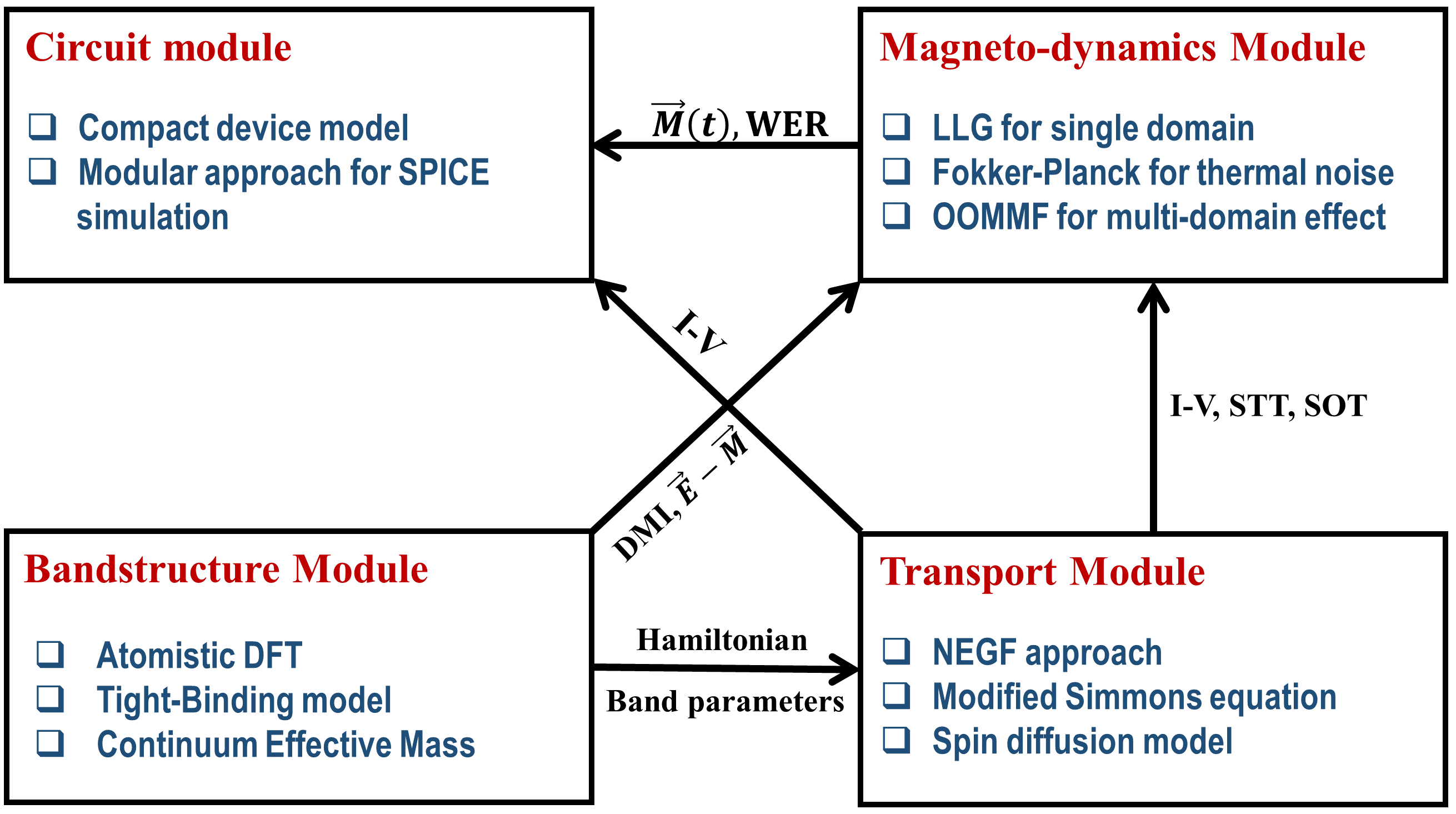
To understand and resolve these challenges, a holistic approach is needed that goes all the way from the material physics to the circuit performance. In an earlier article xie2016spin we laid the groundwork, basic equations, derivations and key concepts underlying this approach. Our focus there was on the physics behind switching - the torque and its voltage asymmetry, symmetry filtering by MgO, the resulting high TMR and its depolarization by oxygen vacancies, and ‘first principles’ spin torques based on Density Functional Theory (DFT) for various materials. The aim of this review article is to focus on the device performance end - i.e., evaluate a few proposals to mitigate challenges at every level, from material to device to circuit.
Fig.2 illustrates the multi-scale computational approach. At the material level, we describe the electronic bandstructure of the magnetic contact using atomistic density functional theory (DFT), or a phenomenological continuum model with well benchmarked parameters. These bandstructures allow us to navigate a large phase space of unexplored magnetic materials beyond a few mature material systems, sometimes with opposite design criteria. For example, STT devices need a high spin polarization, low damping and low saturation magnetization for efficient current induced switching, and a high magneto-anisotropy to maintain adequate energy barrier for retention. For voltage driven switching in multiferroic materials on the other hand, we need a low anisotropy field to write easily along the hard axis, and a correspondingly high saturation magnetization to restore the energy barrier. In section 4, we will discuss an example of material engineering involving a high throughput computational study on the Heusler compounds to identify materials with high spin polarization, and layered Heuslers to engineer added magnetic anisotropy.
The transport module calculates the current-voltage (I-V) characteristics and the spin transfer torque from the magnet and oxide bandstructures - atomistic or continuum. Ballistic transport in MTJs can be calculated using the Non-Equilibrium Green’s Function (NEGF) method (section 5) ghosh2015nanoelectronics , whereas spin transport across larger films such as GSHE or Topological Insulator surface states is described by spin diffusion models. The spin torque is then fed into a magnetodynamics module while the current-voltage (I-V) can be parameterized and used in circuit simulations. Some emerging devices such as those based on multiferroics or skyrmions in magnetic insulatorsWhite2012 , may not need a charge current. In those cases, the coupling between the ferromagnetic and ferroelectric orders can be extracted from material modeling and directly fed into the micromagnetic simulations.
At the magneto-dynamic level, the stochastic Landau Lifshitz Gilbert Slonczewski (LLGS) equation describes the dynamics of small magnets in the presence of current driven torque and thermal noise, while the corresponding Fokker-Planck equation directly calculates the nonequilibrium spin probability distribution. Further complications can arise from transient dynamics that may involve incoherent switching with sub-volume excitations. We discuss stochastic magnetization switching in section 6.
Finally at the highest level, simple compact models (section 8), or more general modular circuit models (section 9) incorporating material parameters can be used to simulate a complex architecture and study the interactions among various devices in the circuit. Such a modular approach relies on Kirchhoff’s laws for charge current and their relations with the non-conservative spin currents. Ultimately, the merit of this unified toolbox is that it connects the material study all the way to the device/circuit performance metrics approaching a system level analysis, or vice versa - reverse engineering from desired performance criteria back to material optimization.
4 Material optimization - searching for half-metals in the Heusler family
Although ultra-high TMR was observed under laboratory conditions, the need to reduce resistance area (RA) for impedance matching, and therefore the insulator thickness, reduces the TMR dramatically in practical applications. The development of novel materials is critical to attaining a high TMR ratio beyond . This requires a highly spin-polarized magnetic layer in an MTJ. One type of material predicted to have high spin-polarization is a ’half-metal’ in which the electronic structure of one of the spin channels is metallic while the other is semiconducting. For Fe and FeCo, this happens to be the band with orbital symmetry given by s, pz and d along the transport z direction. Thus an extremely large TMR is expected to occur in MTJ using half-metals as electrode materials, coupled with MgO which filters out other non- bands through orbital symmetry. The high TMR follows from the fact that electron tunneling is significantly reduced in the anti-parallel magnetization configuration and reliant on minority spin tunneling.
Although a large number of half-metals have been predicted by first-principles calculations PhysRevB.66.134428 ; PhysRevB.51.10436 ; tobola2000electronic ; kandpal2006covalent ; galanakis2006electronic , these discoveries appear to occur mainly through serendipity. Furthermore, it is not clear which of the many half-metals that can be imagined, are stable. Thus, a systematic study of the structural stability of half-metals should provide guidance for future experiments. Here we describe a rational approach to design body-center cubic (BCC) half-metallic structures called “Heusler compounds”butler2011rational . We also investigate the stability of these compounds through the calculation of their formation energies and the comparison of these calculated energies to the calculated energies of other possible phases, and combinations of phases PhysRevB.95.024411 .
4.1 How to design a half-metal
To explain the origin of half-metals in the Heusler family, we need to start from a 1D atomic system with two different atoms, and , as shown in Fig.3. We assume different on-site energies of the orbitals for sites and sites, and (), respectively. If we only consider the first-nearest-neighbor interaction, the 1D atomic chain can be described by the tight-binding Hamiltonian for the periodic array of dimers:
| (1) | ||||

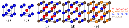
where is the coupling between nearest neighbor atoms. Assuming periodic boundary conditions and invoking a plane wave solution (Bloch’s theorem) , we can get a band gap extending from to with bandgap . This gap is independent of the hopping term, , letting us easily extend the 1D chain to 3D body-center cubic B2 structuresPhysRev.94.1498 ; butler2011rational . B2 structure can be viewed as alternate atomic layers along (001) direction only with nearest neighbor interactions (As shown in Fig. 4(b)), but there are no intra-layer interactions. This means that the wave vector perpendicular to the (001) plane, , generates an expression identical to the 1-D dimer expression above, resulting in a gap between and . Since the gap between and is not dependent on , the gap will remain after integration over .
In order to create half-metallic ferromagnets, we can select different transition metal elements with orbitals on the and sites. As long as the interactions are restricted to nearest neighbors, we can predict that there is still a gap between the onsite energy for the sites and the onsite energy for the sites for a B2 structure.
If we assume the onsite energy is determined primarily by the onsite electron number, then we see that the system can lower its energy if it enhances the size of the gap by increasing the difference in the number of electrons for and atoms, so that the Fermi energy falls inside the gap. The outermost electronic states that participate in hybridization in B2 compounds are a single and five orbitals, so we have nearly six bonding states below the Fermi energy. In other words, there are a total of six electrons in the gapped spin channel. We thus end up with an approximate thumb rule for these compounds: in the gapped spin channel, the approximate electron count on alternate atoms and must be four and two (the ‘4-2’ rule) butler2011rational . If the total valence electron number is twelve, it is easy then to create a semiconductor since each spin channel has six electrons. By making the total valence electron number larger (or smaller) than 12, the majority (or minority) spin channel will now be ’doped’ to be metallic, while the other spin channel remains semiconducting since the Fermi energy falls in the gap.
While the above design rule seems compelling, first principles calculations indicate that the B2 structure only achieves a pseudogap instead of a true gap. This is because of residual next nearest neighbor (NNN) interactions butler2011rational that were not included in our consideration so far. To reduce the NNN interactions, we can replace one transition atom with a main group atom without any d-states, acting as a ‘spacer’ - resulting in the full-Heusler family of compounds (Fig.4 c). Furthermore, We can delete half of the atoms to generate half-Heusler compounds with a ‘cleaner’ gap (Fig.4 d). We can also exchange the position of atoms and atoms to generate inverse-Heusler compounds (Fig.4 d). In all cases, the decreased NNN interactions will narrow the bands and prevent the density of states from tailing into the gap.
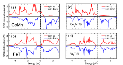
To confirm this rational design approach, We performed all calculations using Density-Functional Theory (DFT) as implemented in the Vienna Ab-initio Simulation Package (VASP) Kresse199615 to calculate the density of states for CoMn and FeTi in the B2 phase. Rather than a gap, we find a deep, wide minimum in the minority spin density of states at half-filling which we refer to as a pseudogap, with 3 electrons per atom under the Fermi energy. For the pseudogapped channel, the “4-2 rule” forces atoms (Fe or Co) to hold 4 electrons and atoms hold 2 electrons. As we replace one Mn or Ti with a Si spacer, the pseudogaps in B2 systems turn into real gaps, resulting in the half-metal Co2MnSi and semiconducting Fe2TiSi. For these two full-Heusler compounds, the spacer Si atom also holds 2 electrons in the gapped channels to sustain the ‘4-2’ rule. We can thus create half-metals by turning B2 compounds into Heusler compounds.
Based on this idea, a large number of layered half-metallic structures can be obtained in full-Heusler, half-Heusler, and inverse-Heusler family. Let us discuss half-Heusler compounds in the next section.
4.2 Half-Heusler compounds
In this section, we review our computational investigation covering 378 half-Heuslers (with Cr, Mn, Fe, Co, Ni, Ru, Rh; Ti, V, Cr, Mn, Fe, Ni; Al, Ga, In, Si, Ge, Sn, P, As, Sb) as calculated by VASPPhysRevB.95.024411 . The crystal structure of half-Heuslers is shown in Fig.4 (d).

If we consider upto NNN interactions, the nearest-neighbor couplings will only occur between and atoms. Since the four orbitals from the main group element hybridize with a lower energy level, the origin of the gap in the gapped spin channel comes from the hybridization between the five states of the higher valence and the lower valence transition metal atoms and . As the Fermi energy falls in the gap, there are a total of states being filled in this spin channel (as shown in Fig.6). Since the spin moment per atom is just the difference in the number of up and down electrons per atom (), and since , with 9 states fully occupied in the gapped channel () we get the simple ‘rule of 18 for half-metallicity in half-Heusler compounds:
| (2) |
where is the total magnetic moment and is the total number of valence electrons per XYZ formula unit. If the total valence electron number is 18, the system will tend to be semiconducting with 9 electrons under the Fermi energy per spin channel. If the total valence electron number is not equal to be 18, one spin channel may be ’doped’ to be metallic while the other spin channel remains semiconducting, resulting in a half-metal. We find from our computational results that all the semiconductors and half-metals in the half-Heusler family do follow this simple Slater-Pauling rule precisely with integer total moments.
We further investigate the energetics of 378 half-Heusler compounds in the cubic structure to ensure their stability. For each XYZ half-Heusler compound, we calculate its formation energy using Eq. 3 and distance from the convex hull using Eq. 4.
| (3) |
| (4) |
where is the total energy per atom of the half-Heusler compound, is the reference chemical potential of element , chosen to be consistent with those used in the OQMD database (See Ref. oqmd_npj_2015 for details), and is the lowest formation energy at the composition of all the known phases. A negative value of indicates that at zero temperature, the half-Heusler compound is more stable than its constituent elements. However, it does not guarantee the stability of a half-Heusler phase over another competing phase or a mixture of phases, which is where the Hull distance comes in.
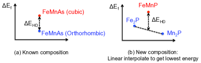
A measure of the thermodynamic stability of a phase is its distance from the convex hull. We utilize the formation energy data from OQMD to do the phase competing analysis oqmd_npj_2015 ; ADMA:ADMA200700843 ; AENM:AENM201200593 . In Fig.7 (a), the hull distance for cubic FeMnAs is the formation energy difference between the cubic phase and the orthorhombic phase, which has the lowest formation energy at that chemical composition. In Fig.7 (b), although we don’t have available the formation energy of other phases at that chemical composition, we can still estimate stability using the hull distance for cubic FeMnP by defining the hull energy () as a linear combination of formation energies of nearby phases Mn2P and Fe2P. By comparing with reports for hull distances of experimentally synthesized ternary compounds, we conclude that a Heusler compound with 0.1 eV has a strong likelihood of experimental synthesis PhysRevB.95.024411 .
From our calculations, we discovered 26 semiconductors and 45 half-metals with negative formation energy. All the half-metals (listed in boxes and square symbols in the green ovals surrounding the dashed lines) and semiconductors (triangles in the gray circle at the base of the dashed lines) are summarized in Fig.8 and all follow the Slater-Pauling rule (Eq.2) precisely. All the other magnetic/nonmagnetic metals are marked out in the purple and yellow areas. 17 out of the 26 semiconductors are identified with 0.1 eV, including 3 likely candidates for fabrication (CoVSn, RuVAs, and RhVGe) that have not been experimentally reported so far. Furthermore, 11 half-metals are identified with 0.1 eV. 9 of these have already been experimentally synthesized in bulk, albeit not in a half-Heusler phase, but they may be synthesized in thin films by molecular-beam epitaxy (MBE). Among the two remaining half-metals, NiMnSb has been verified as a half-Heulser compound with half-metallic characteristics in bulkPhysRevB.42.1533 . Although CoVSb has also been well established in a cubic phase, the compound is a weak itinerant ferromagnet rather than a half-metalCoVSbMag ; CoVSbNeutron . As a result, only one half-metal RhVSb with 0.103 eV can be predicted as a good candidate for future experiments.
While the half-Heusler family ultimately produced few stable half-metals, in hindsight this is not hard to understand because the XYZ cubic structures are not close packed and contain a vacancy sublattice, which compromises their stability. Based on our studies, we expect the full-Heusler family to yield a larger number of stable half-metals.
4.3 Non-magnetic spacer engineering - symmetry filtering of MgO
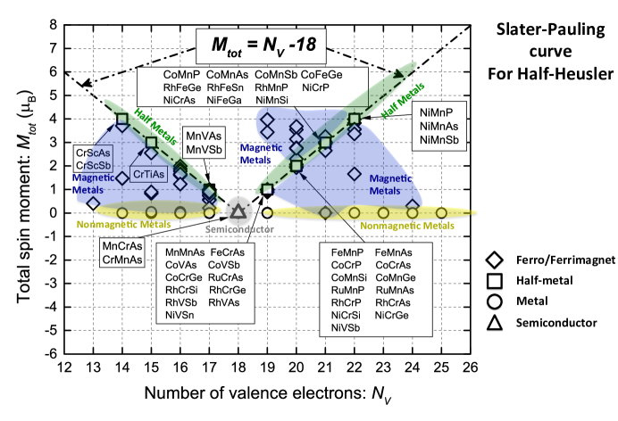
The other important material choice for the magnetic tunnel junction is the nonmagnetic spacer. One of the important developments in MTJ technology was the adoption of MgO as the spacer material in magnetic tunnel junctions. As predicted in Fe/MgO/Fe junction from the first-principle calculationsbutler2001spin , the reason why MgO performs much better than the common earlier as the insular in MTJs is due to the symmetry filtering effect. When the propagating states in Fe hit the MgO, these wavefunctions continue inside the bandgap of MgO as decaying waves. The continuation requires the conservation of symmetry from the Fe states to the MgO states. In MgO, different states have different decaying lengths. In particular, the complex band in MgO needs to connect the conduction and valence bands with similar orbital constitutents, which results in a shorter wavelength (longer decaying length) near the mid-gap than the simple WKB theory predicts. In an Fe/MgO/Fe magnetic tunnel junction, the Fermi energy lies near the mid-gap of MgO, as shown in Fig.9. As a result, other Fe bands are filtered out and leaves the Fe band with the highest transmission through MgO, dominating the tunneling current. As it turns out, the Fermi energy only crosses the Fe band in one spin channel, which essentially makes Fe a half-metal to MgO. A more detailed discussion about symmetry filtering can be found in ref.butler2001spin ; xie2016spin . Noted that in practical devices CoFe is better than pure Fe because of anisotropy and magnetostriction, but the same symmetry filtering mechanism applies.
Note that MgO is particularly critical to the performance of MTJs built from non half-metallic magnetic electrodes such as Fe and FeCo, where multiple bands cross the Fermi energy. In these MTJs, symmetry filtering is needed to remove all but the band, which alone needs to be half-metallic. For intrinsic half-metals on the other hand such as the Half-Heuslers described earlier, we seek instead to find any insulating spacer that preserves its half-metallicity. MgO might also satisfy that function in some cases, for instance with NiMnSb as we show in section 5. In the next section, we will discuss another class of insulators that may offer better opportunities for maintaining the half-metallicity of Heusler half-metals - namely Heusler semiconductors. Combining a Heusler metal with a lattice matched Heusler semiconductor brings in another advantage - creating a uniaxial anisotropy, which is also important in nanomagnetic applications. The combination of different Heusler alloys opens the possibilities of better engineered heterojunctions for spin transport. In fact, the metallic ’All-Heusler’ spin valves have already been investigated for enhanced current-perpendicular-to-plane giant magnetoresistance effect (GMR)nikolaev2009all; li2016current.
4.4 All-Heusler superlattice: half metals with uniaxial anisotropy
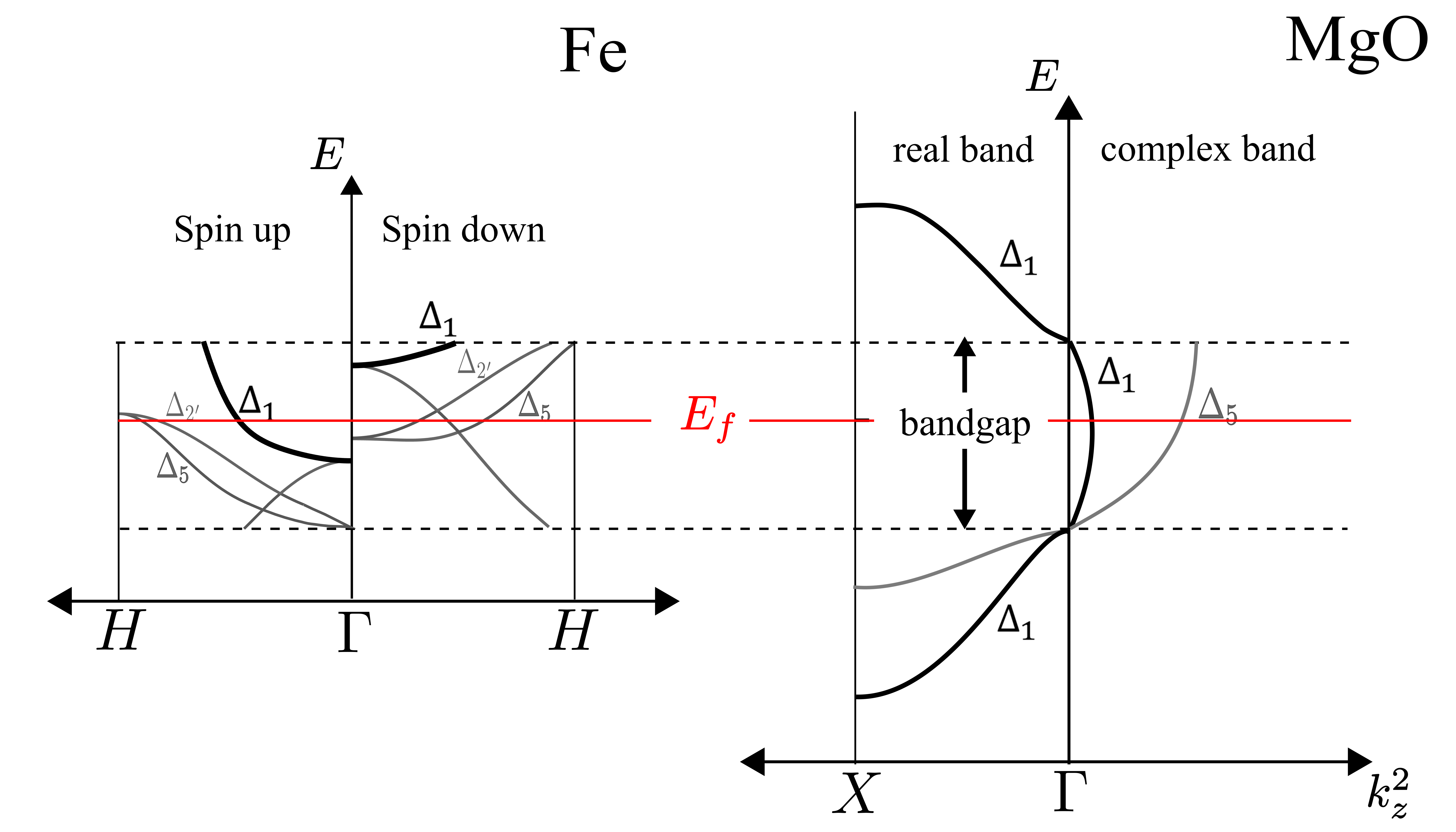
One drawback of Heusler compounds is that the symmetry of their cubic crystal structure compromises their uniaxial magnetocrystalline anisotropy (MCA), needed to create a large enough energy barrier for spin retention. However, our study unearthed several half-Heusler compounds that were not only half-metals, but also semiconductors, many with very similar lattice constants. This is an important factor because half-metallicity arose from the specifics of the underlying crystal structure and chemistry, and extending that crystal structure in a heterojunction helps maintain the half-metallicity of the candidate Heuslers. Indeed from first-principles calculations, we show that by making layered superlattices of two Heusler compounds, an intrinsic uniaxial anisotropy can be achieved heuslersuperlattice while maintaining the half-metallicity. This uniaxial anisotropy is generated by the different electronic configurations of the two Heusler compounds and by the distortion of the lattice, which causes the local environment of each atom to be different in the direction perpendicular to the layers from that in the plane of the layers. We find that some of the Heuser superlattices layered perpendicular to the [001], [110] and [111] directions do retain their half-metallicity. We find this to be true for full-full, half-half and full-half Heusler combinations.
In short, some of the designed superlattices combine half-metallicity with perpendicular magnetic anisotropy. For example, the Co2TiGe-Fe2TiGe superlattice layered along the [100] direction (shown in Fig.10) can retain half-metallicity with a perpendicular anisotropy of J/m, while the Co2MnSi-CoTiSi superlattice layered along the [110] direction retains its half-metallicity with perpendicular anisotropy of J/m. More details are discussed in refheuslersuperlattice . Such PMA half-metallic superlattices or thin films can be quite competitive as a material stack for an STT-MRAM device.
5 Transport in nanostructures with NEGF
5.1 Non-equilibrium Green’s Function (NEGF) approach
Charge Current in Nanostructures.
NEGF is a powerful tool to study the quantum transport phenomenon in nanostructures such as the magnetic tunnel junctions. In a two-terminal device, the charge current can be evaluated using
| (5) |
where is the bias dependent transmission between the left and right electrodes at a given energy . are the Fermi functions of the left and right electrodes respectively. is the retarded Green’s function and are the electrode coupling matrices given by:
| (6) |
where is the Hamiltonian of the system and are the ‘self-energies’ that account for the projected bands and level broadenings by the two semi-infinite electrodes ghosh2015nanoelectronics ; datta2005quantum ; rocha2006spin .
Spin Current and spin transfer torque
One can use the NEGF equations to calculate the spin current and spin transfer torque as well. The spin torque can be calculated from the time evolution of the magnetic moment of electron , which is derived from the Schrodinger equation, , :
| (7) |
where the spin operator and are the Pauli matrices. is the electron correlation function describing the occupancy of the states. The spin current between two sites and can be extracted from the torque expression asghosh2015nanoelectronics ; theodonis2006anomalous :
| (8) |
The above equation works for systems with orthogonal basis. For non-orthogonal basis, an additional overlap matrix should be included in the formalism. Details can be found in xie2016spin . The calculated spin current can then be used to evaluate the spin transfer torque based on the angular momentum conservation. For example, to evaluate the STT on the free magnetic layer of the MTJs, we calculate the incoming spin current at the oxide-magnet interface. We can then assume the spin current coming out from the other side is already fully polarized along the magnetic moment of the free layer, implying that all the angular momentum perpendicular to the free layer has been absorbed, which equals the spin torque exerted on the free magnet.
5.2 ab-initio transport calculations
Coupling NEGF with DFT allows parameter-free first principles calculation of the I-V characteristics and the spin transfer torque of the magnetic tunnel junction. As previously discussed, the high throughput computational studies of Heusler compounds have provided us with a large pool of potential materials for nanomagnetic applications. These half-metals are critical to build effective MTJs with high TMR ratio. To investigate whether their half-metallicity can be preserved in an MTJ configuration, and to quantify how much STT and TMR a Heusler-based MTJ or an all-Heusler superlattice can generate, we need to move from electronic structure to nonequilibrium transport calculations. For an MTJ structure for instance, we can use LLGS to get the macrospin dynamics in presence of a drive current, but to relate that current back to an applied voltage, we will need to calculate the current-voltage (I-V), with barrier heights, contact densities of states and orbital effective masses of the tunneling electrons extracted from DFT. We use the numerical atomic orbital-based DFT program SIESTA that combines DFT with the Non-equilibrium Green’s Function program Smeagol to calculate the I-V characteristics and the spin transfer torque of a magnetic tunnel junction from first principles xie2016spin ; rocha2006spin ; soler2002siesta .
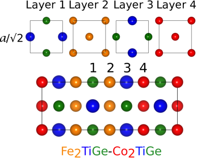
Fig.11 shows an example calculation on the half-metallic NiMnSb-MgO(5ML)-NiMnSb junction. The interfacial structure is chosen from the lowest energy configurations with the inter-atomic distance averaged from a fully relaxed structure. The ultra-high TMR () indicates that the half-metallicity is well preserved in an MTJ even in the presence of interfacial strain and applied bias. The calculated TMR is most likely overestimated because of the adoption of a ballistic transport model across the MgO (predominantly driven by tunneling). We do not include any spin-flip scattering in our current calculations at this time. Since is a small number, a tiny amount of scattering could vastly degrade the TMR. In principle, the defect induced spin scattering can be included in the calculation, but that requires prior knowledge of the type and location of depolarizing defects in the MTJ and the exact interface morphology. For example, we reported the impact of oxygen vacancies on TMR degradation in Fe/MgO/Fe MTJs in xie2016spin . We found there that the TMR is particularly compromised if the vacancy sits close to the oxide-magnet interface. We can include incoherent spin scattering in transport calculations by representing the ensemble of the scattering events with a self-energy term in NEGF in the Born approximation, describing their average effect on the transport Yanik2007 . This method however needs prior microscopic knowledge of the spin scattering potential at a given interface morphology.
5.3 Spin amplification in Topological Insulators
High spin-polarized magnetic electrode materials are critical to the improvement of the TMR ratio and the readability of nanomagnetic devices. Increase in spin polarization also improves the write performance in STT-MRAMs. However, without a spin-to-charge gain, it is hard to reduce the write current beyond a limit set by conservation of spin angular momentum between the conduction electrons and the magnetization of the electrode.
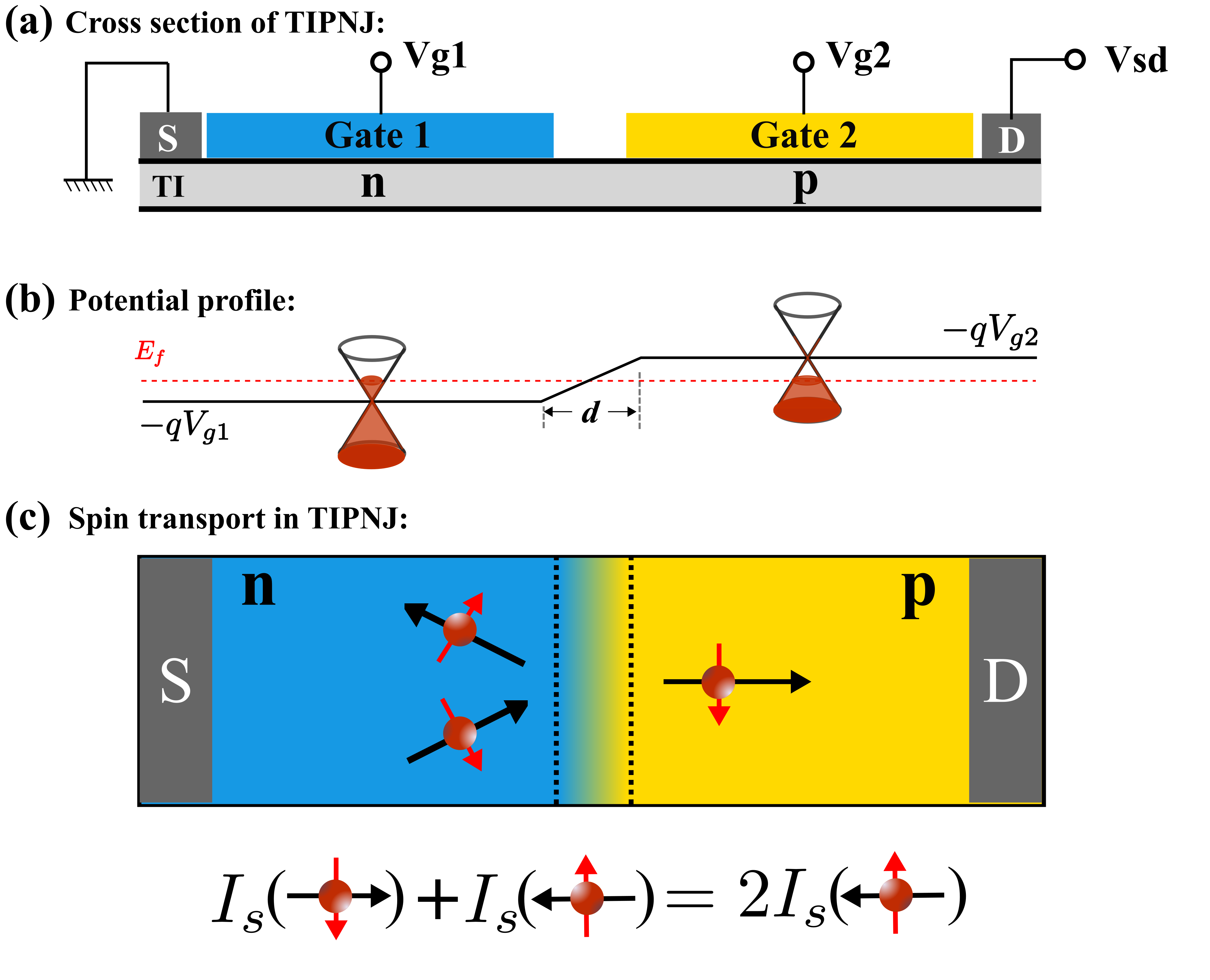
One possible way to achieve spin-to-charge gain is through 3D topological insulator surface states. For instance, we can use a gate controlled PN junction on a TI surface to control the spin-to-charge conversionhabib2015chiral . Fig.12 illustrates the idea of spin amplification at a TI PN junction. The TI surface is electrostatically doped into an N region and P region by top gates. An NEGF simulation based on a parameterized TI surface Hamiltonian shows that the PN junction acts like a ‘collimator’, where only electrons with small incident angle with matching spins are allowed to tunnel through the junction. This collimation follows the physics of Klein Tunneling of Dirac fermions, also observed for pseudospins at a graphene PN junction. On the source side, most electrons with large incident angle are reflected back with their spins flipped due to the spin-momentum lockingqi2011topological of the TI surface states. While the charge current is reduced due to the backscattering of electrons, the spin current is amplified because of the simultaneous flip of momentum and spin.
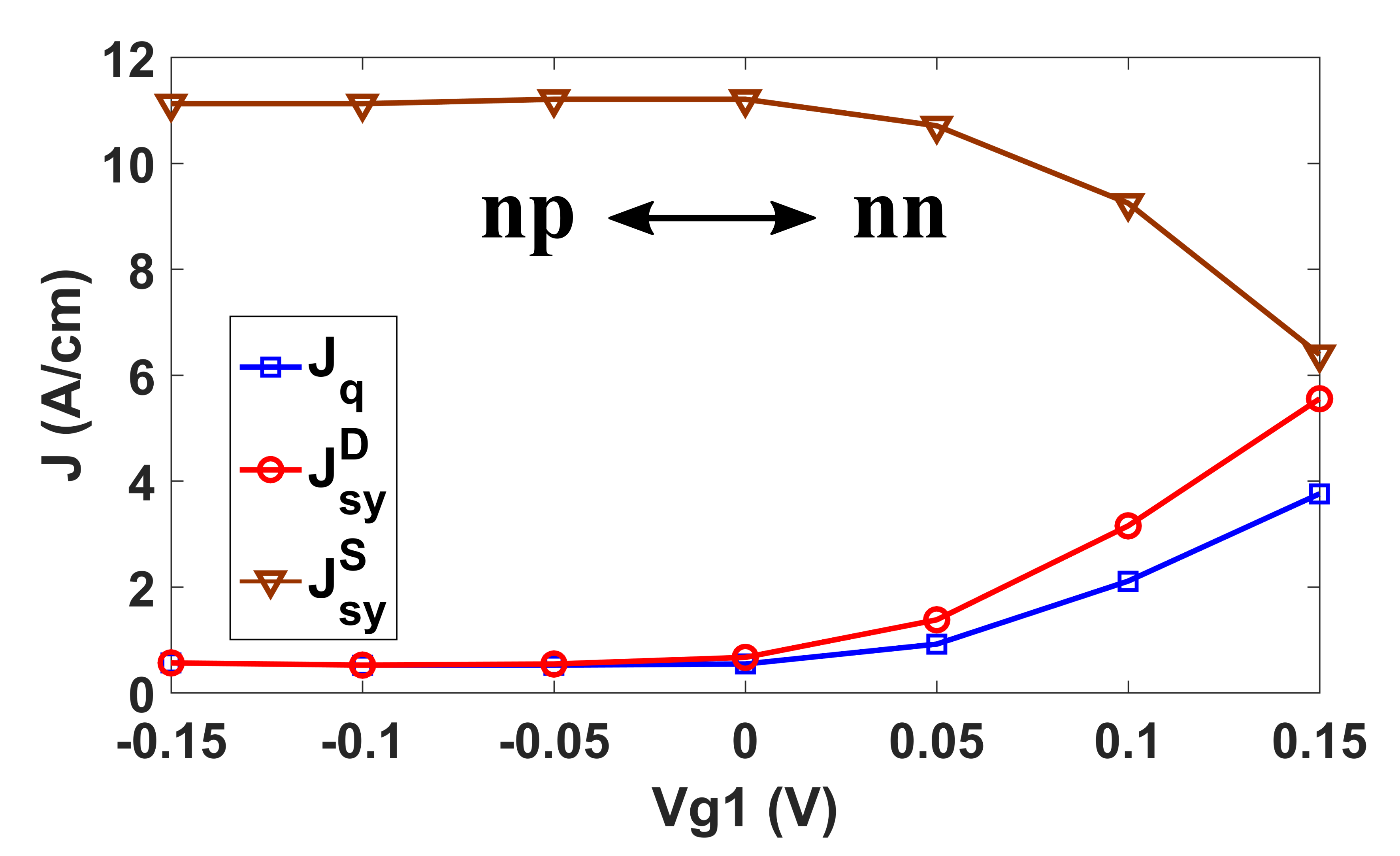
Fig. 13 shows the NEGF simulation of the charge/spin transport on TI PN junction. The simulation result indicates a spin-to-charge gain that can be tuned by the gate voltage from to as high as (compared to in usual GSHE through the geometrical gain). The large gate tunable spin to charge conversion is potentially useful for charge spin logic behin-aein_proposal_2010 . However, it is worth emphasizing that the transport focused exclusively on the surface conduction on TI. A more detailed model is needed to explore the spreading resistance of the surface currents into the bulk, to quantify any additional leakage of spin current.
6 Magnetization dynamics: stochastic vs deterministic switching
Once a spin polarized current enters the soft magnet, the spin torque tries to destabilize the magnetization, making it precess for small currents and eventually reversing the magnetization beyond a critical current. The dynamics is complicated and involves the current driven torque, the Gilbert damping that tries to reset the magnetization back towards its equilibrium value, and various real and pseudo-magnetic fields that arise from the potential that the spins swing in - from external fields, shape and magnetocrystalline anisotropy, as well as thermal noise. The effect of thermal noise is particularly important. When the applied current is slightly below the critical current , thermal excitation dominates the switching. At equilibrium (zero current), random kicks from the thermal noise create a probability distribution of the initial magnetic moment. These thermal fluctuations help the switching process by knocking the spins out of ‘stagnation’, when the two magnets are momentarily locked into a state with precisely parallel or antiparallel magnetization (i.e., zero torque). Subsequently, thermal fluctuations hinder the smooth ballistic flow of spins under spin torque by creating occasional thermally induced backflips.
The evolution of magnetization under spin transfer torque can be described by the Landau-Lifshitz-Gilbert-Slonczewski (LLGS) equation:
| (9) |
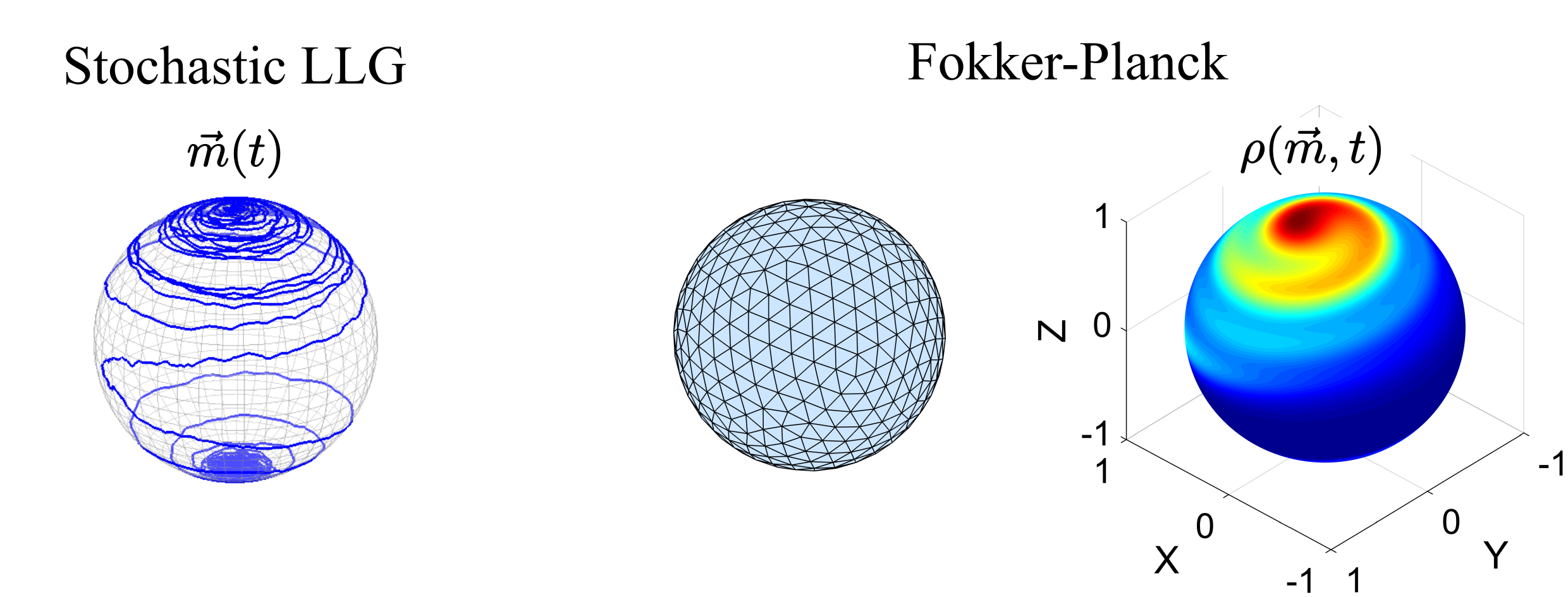
where is the in-plane (out-of-plane) spin transfer torque, is the magnetic damping coefficient, is the permeability constant and is the gyromagnetic ratio. In PMA systems, the out-of-plane torque can be ignored and the in-plane torque can be approximated as where is the charge current and is the unit vector along the direction of the polarized spins, is the volume of the magnet, is the saturation magnetization and is the electron charge. includes the external magnetic field, the anisotropy field, and the demagnetization. To describe the effect of thermal noise, a noise field is also included in the effective field , where is a three-dimensional Gaussian white noise uncorrelated in time and space. From the LLGS equation one can work out the zero temperature critical current (for PMA) where is the thermal stability factor and is the effective magnetoanisotropy that includes the intrinsic anisotropy and the demagnetization along the perpendicular direction. Fig. 14(left) shows the initial stagnation of the spins until thermal fluctuations dislodge them, and the subsequent evolution of the spins under the action of the current torque along with a superposed thermal jitter. It is worth mentioning that describing the magnet dynamics with a single LLGS equation assumes coherent switching, which works for magnet with size smaller than its exchange length. For a large magnet, the magnetization switching is mostly incoherent. Describing such complicated processes usually requires full micromagnetics simulations. Section 6.3 summarizes some efforts to approximate the incoherent switching effect within macrospin framework.
6.1 Fokker-Planck equation
An alternative way to describe the stochastic switching behavior is through the Fokker-Planck equation (FPE). Instead of keeping track of the noisy trajectory of the magnetic moment under thermal jitter, the FPE solves directly for the probability distribution of the magnetic moment . Under the macrospin assumption, the amplitude of the total magnetic moment is conserved. can then be solved on a 2D spherical surface (Fig.14 right). Brownbrown1963thermal first applied the FPE method to study the thermal excitation in single domain magnets.
It is straightforward to extend FPE to include spin transfer torque. We can derive the Fokker-Planck equation starting from the stochastic LLGS equation, assuming an uncorrelated Gaussian white noise for the thermal scattering processes ghosh2015nanoelectronics . The Fokker-Planck equation can be expressed in a general form:
| (10) |
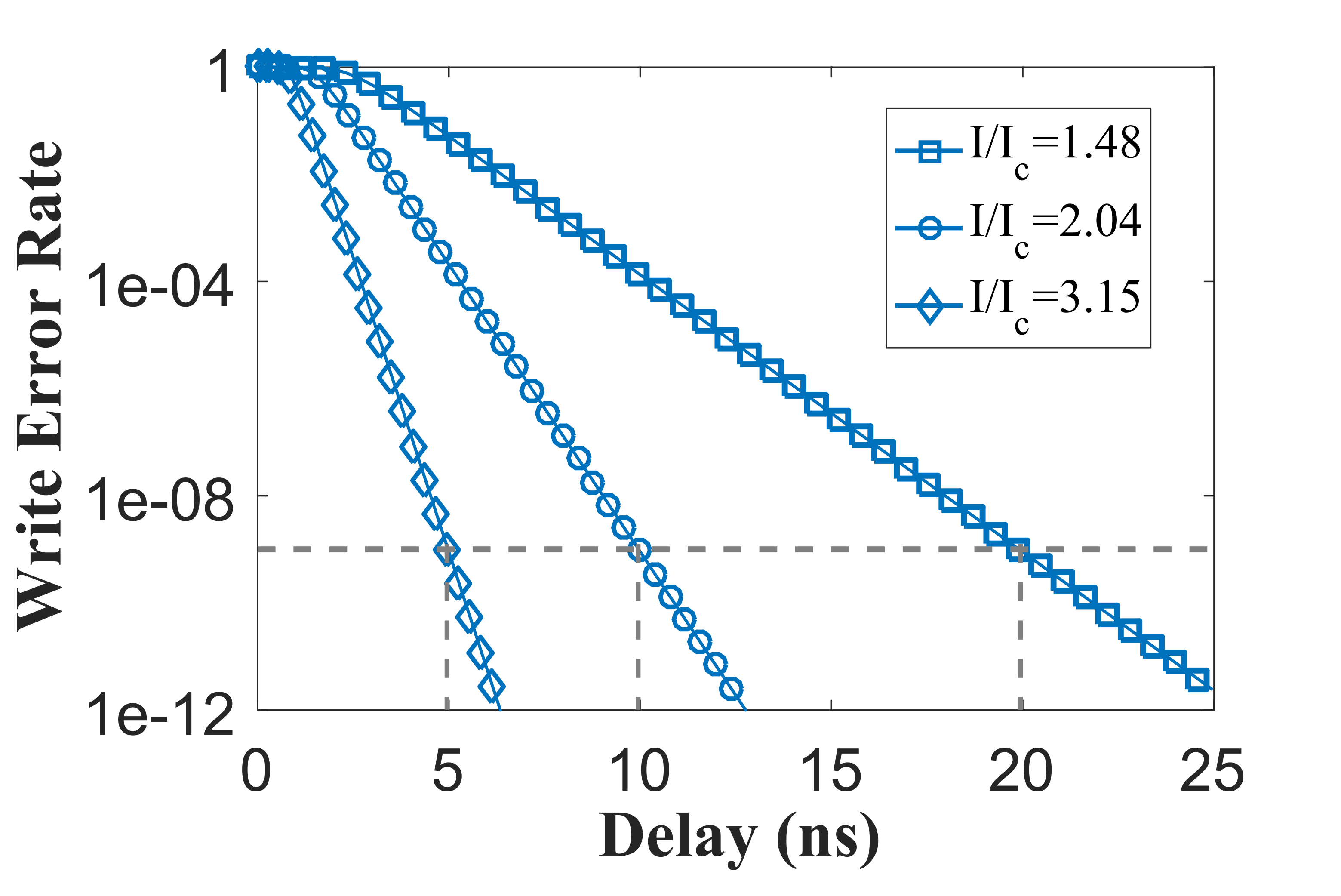
where is the sum of all the deterministic torques from the right side of Eq.9. is the effective diffusion coefficient that captures the effect of thermal noise. Fig. 14(Right) shows the evolution of the entire probability density function over time. Fig.15 shows a typical plot for the write error rate (WER) as a function of the switching delay for varying degrees of overdrive current.
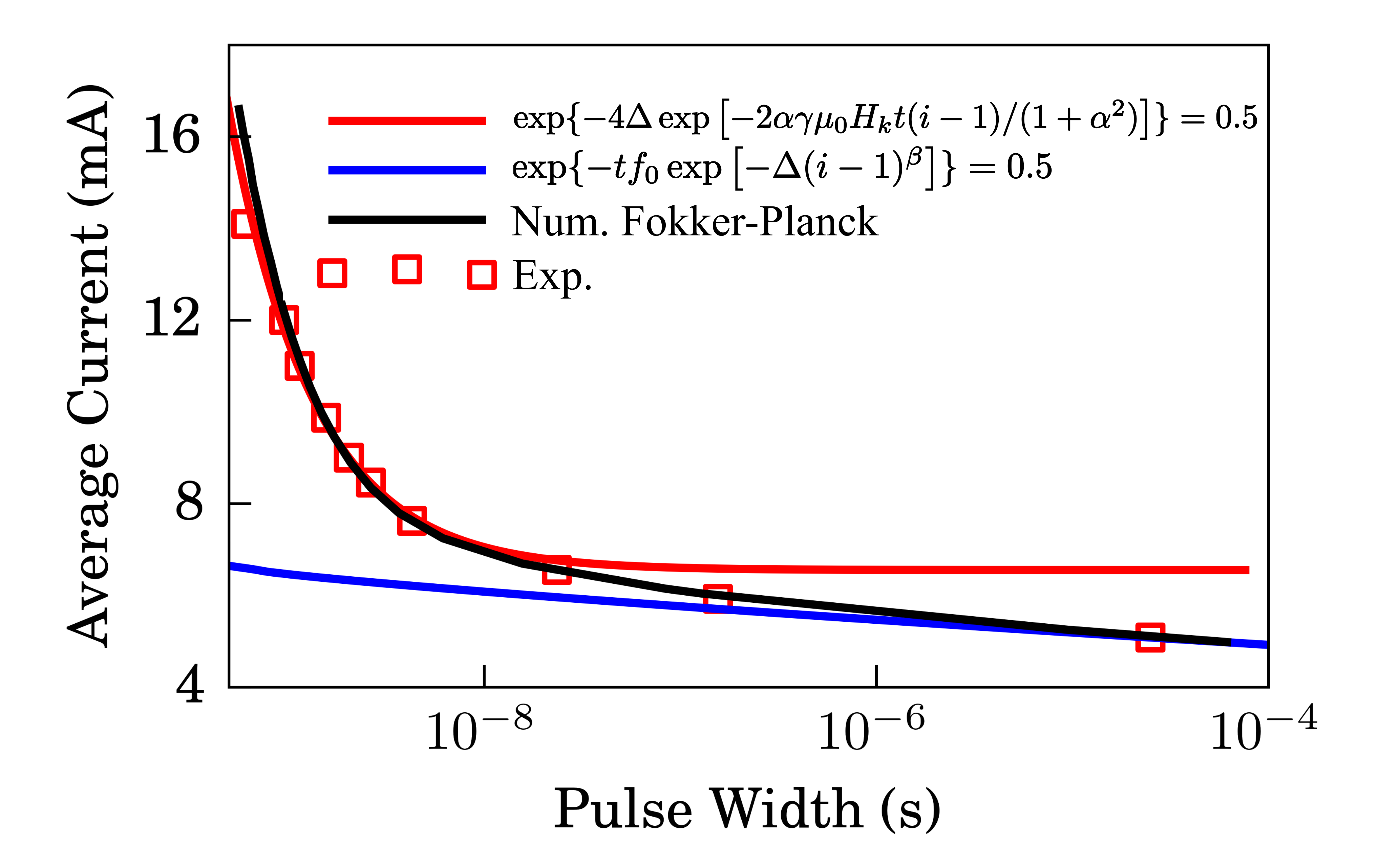
The FPE and stochastic LLGS methods are formally equivalent, for magnets driven by uncorrelated white noise. However, there are two practical advantages of the FPE approach: first, the FPE is a deterministic equation that can be solved more efficiently than the stochastic LLGS equation, especially for statistical quantities such as averages and standard deviations (rare events can also be captured by the tail of but need a hyperfine grid). The one-time solution to Eq.10 gives the statistics of the ensemble of most likely switching events. Second, it is possible to obtain analytical solutions to the FPE under certain simplifying conditions. For example, the Fokker-Planck equation reduces to a 1-D differential equation in cylindrically symmetric systems such as the PMA MTJs. The analytical solutions can then be worked out when the applied current is in either the sub-threshold () or the super-threshold limit () butler2012switching . In a more general case, the FPE can be solved numerically on a spherical surface using the finite element method and can be shown to bridge these limits seamlessly xie2017fokker . Fig.16 shows the comparison between the fittings from the numerical FPE and two other widely used analytical models in the literature.
It is instructive to look at the relation between the WER and the total charge flowing through the magnet, which can be calculated approximately from the Sun’s equation shown in the inset of Fig. 16 and Eq. 13. From the write-error rate WER, we can get the following equation
| (11) |
which means that the efficiency of switching ultimately depends on the total accumulated charge , and we can ramp up the accuracy by overdriving with charge exceeding the minimum critical charge to destabilize the spins towards flipping. The critical charge is obtained from simple angular momentum conservation, trading off the spin with that from the magnets , while accounting for partial polarization of the tunneling electrons (making them less efficient by a factor ), and the damping correction implying that part of the injected spin leaks out into the environment. For a magnet of size nm nm with about 100,000 spins, we need about 106 electrons to provide the critical charge . For a ns switching time, this already requires a current density of MA/cm2.
6.2 Examples: ‘Tilted’ magnetization for fast switching
As discussed earlier, one obstacle to fast, reliable spin torque switching in conventional magnetic tunnel junctions is the stagnation of the magnetization at points of zero torque. This initial incubation phase of STT plays a dominant role in determining the switching current, speed, and dynamic write error rate (WER). Several solutions have been proposed to overcome the stagnation point to achieve fast and reliable switching. One way to overcome this issue is a non-collinear alignment between the magnetic moments of the fixed layer and the free layer.
Example 1 - orthogonal torque:
One possible way to nudge the magnetization out of its stagnation point is to use an orthogonal spin polarizer, which creates a non-collinear spin injection into the free layer as shown in Fig.17(a). This method was used to achieve fast switching in in-plane MTJs liu2010ultrafast . However, for PMAs there seems to be a trade-off between speed and current density. Fig.17(b) shows a FP simulation of WER as a function of switching delay for collinear and non-collinear spin injections. When the injected current is small, the non-collinear spin injection has a worse WER than the collinear spin injection. The non-collinear spin injection only performs better when the applied current is much larger than the critical current, which is in the dissipative and ultrafast switching regime.
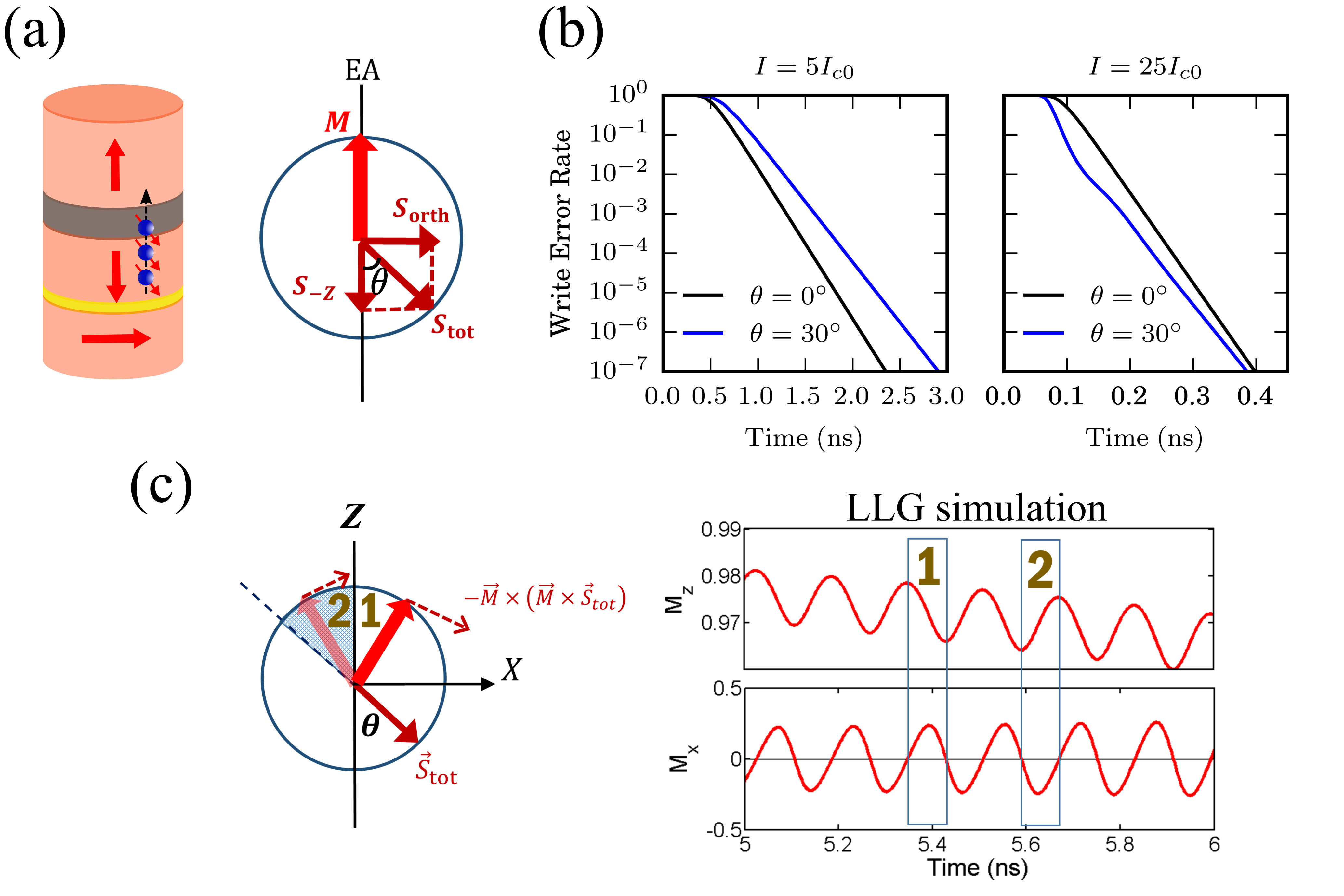
We can understand the trade-off from the schematic figure and LLG simulation in Fig.17(c): at small applied current, the magnetization switching in PMAs is precessional. At a small angle in the initial stage, a non-collinear torque helps to switch (regime 1) in the first half of the precession cycle, but it brings the magnetic moment right back towards its initial state in the second half (regime 2). This can be avoided only when the current is large enough to allow the magnetic moment to cross the equator in regime 1 itself. Such a large current is hard to achieve in an MTJ and creates undesirable dissipation. Other possible ways to generate an orthogonal torque could include a combination of GSHE and STT where the orthogonal torque can be generated from the GSHE without passing a large current through the MTJ.
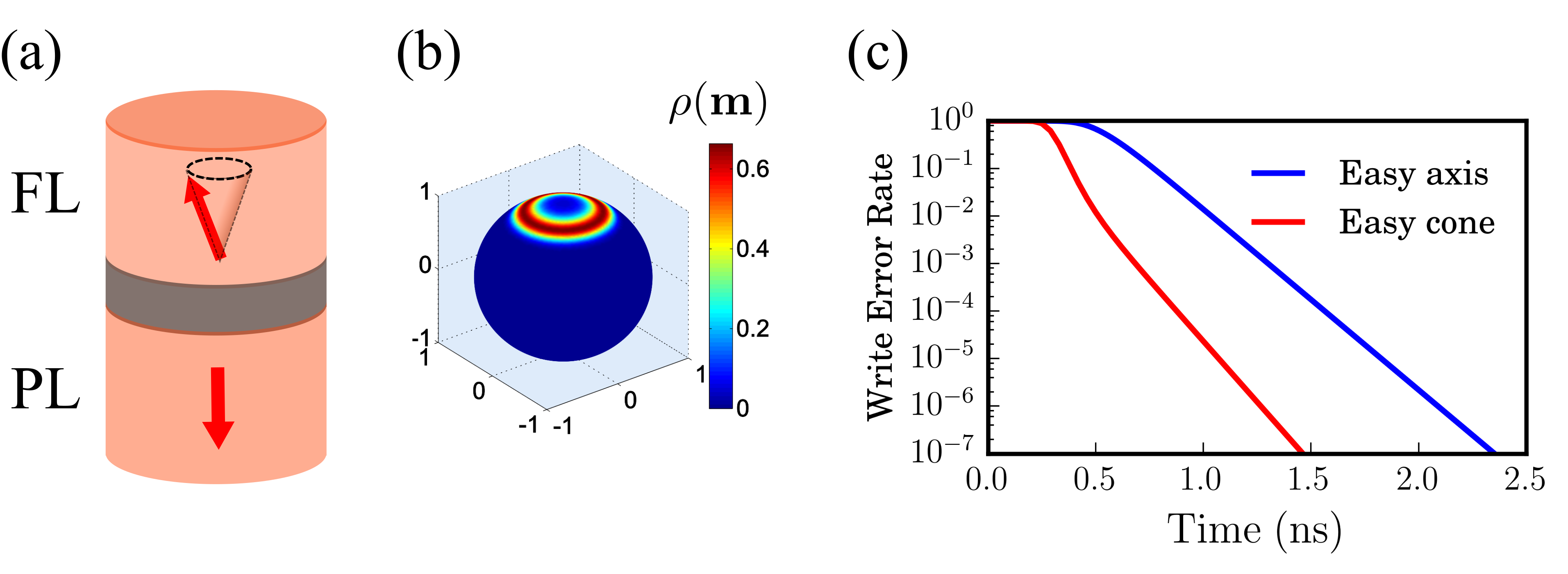
Example 2 - Easy-cone magnets:
The second example of non-collinear alignment is a system with conical magnetoanisotropy. In these systems, the energy profile can be expressed as , where is the sum of all second order anisotropy terms including the usual interfacial perpendicular anisotropy and the demagnetization, while is a higher order anisotropy term. It has been shown that when the free layer is within a certain thickness range, the energy minimum appears along the surface of a cone rather than along the axis shaw2015perpendicular . Fig. 18 shows the FPE simulation of the WER for an easy-cone magnet compared to an easy-axis magnet with the same thermal stability factor . As expected, a ‘tilted’ initial magnetic moment helps reduce the switching time and error. We see a quick initial evolution since the stagnation point of zero torque has been shifted. Subsequently we reach the shifted stagnation point, and after that the evolution slows down, but since the Boltzmann distribution for the easy cone is not along the stagnation point, we still see a faster slope of the WER.
6.3 Non-coherent switching
So far we have assumed that the magnet switches in a coherent way so that all the electron spins are bundled together as one ‘giant spin’. This approximation holds reasonably well for small sized single domain magnets, but there seems to be evidence that the transient response of the spins is not coherent, especially for intermediate sized magnets. A full spatially resolved micromagnetic simulation is needed to describe the complicated magnetization dynamics in these systems. Studies have suggested various possible mechanisms for transient incoherence, such as sub-volume excitation sun2011effect , edge nucleation finocchio2007micromagnetic and global magnetostatic instability munira2015calculation . The general idea behind incoherent switching is that a medium sized magnet is excited by the STT through multiple precessional modes with different frequency and spatial patterns. Among those modes, the simplest is the coherent uniform precession. However, to switch the magnet in a coherent mode requires the magnetic moment to overcome the energy barrier where is the whole volume of the magnet. Micromagnetic simulations suggest several switching mechanisms that only need to overcome a lower barrier height. For example, ref.munira2015calculation suggests a global magnetostatic instability in STT switching in PMAs, where a non-coherent precessional mode starts to destabilize and diverge when the precession amplitude becomes large. Once destabilized, the entire magnet will eventually flip. Therefore, instead of torquing the entire magnetic moment across the equator (), one just needs to excite the magnetization precession to pass the destabilizing angle, which translates into a smaller barrier height. In the thermal excitation regime with STT, which is the regime where non-coherent flow becomes dominant, the anisotropy energy modified by the spin torque at is munira2015calculation . For coherent switching, the energy barrier is given by where is the angle where the anisotropy energy maximizes (no longer at because of STT but at , obtained by globally maximizing . But the instability implies a lower energy barrier height where is the instability angle and . One can then use the modified energy barrier in a macrospin model to evaluate the switching rate and switching error approximately.
7 Emerging Write Mechanisms For Nano-Magnets
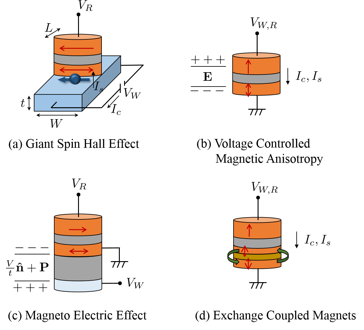
The last half a decade or so has seen an explosion of materials and novel switching mechanisms for manipulating nanomagnets. While ”plain old” STT has already seen commercialization in second generation Magnetic RAMs as STT-MRAMs, these new mechanisms are still experimental and in various stage of commercial development. Some of the experimentally demonstrated materials and phenomena are (Figs. 19, 20)
-
1.
Nano-magnets with interfacial Perpendicular Magnetic Anisotropy (PMA)
-
2.
Giant Spin-Hall Effect (GSHE)
-
3.
Voltage Control of Magnetic Anisotropy (VCMA)
-
4.
Magneto-Electric Switching (ME)
-
5.
Exchange-Coupled Magnets (ECM)
This section briefly describes the physics behind these switches, their intrinsic benefits, and challenges behind each of these materials and/or phenomena. Other mechanisms not discussed here include domain-wall and skyrmion-based devices, piezoelectric/strain assisted switching, magnonic (spin-waves) and thermomagnonic switching.
7.1 Magnets with Perpendicular Magnetic Anisotropy
Physics: A magnet’s anisotropy can be caused by a large number of factors johnson1996magnetic , one of the important being its shape. Magnetic films of elliptical/rectangular profile and thickness of a few nm primarily have their easy axis in the direction of the major axis of the ellipse or long side of the rectangle, with the film plane being the easy plane of the magnet. In each of these descriptions ‘easy’ denotes the direction in which the potential energy is minimum for the magnet. This potential energy profile prohibits the magnetization to wander out to the ‘out-of-the-plane’ axis thermodynamically and is typically included in magnetodynamics calculations as an effective demagnetization field. However, films with circular profiles and extreme thinness () primarily have a high preference for anisotropy in the out-of-the-plane or perpendicular to the plane direction due to surface interactions, especially at the interface ikeda2010perpendicular . This high anisotropy can overcome the demagnetization field and make the perpendicular direction the thermodynamically stable point for magnetization (Fig. 20).
PMA’s have gained a lot of attention recently due to their scalability. Since the magnets are circular in profile and their high anisotropy originates from film thickness, it is lithographically possible to create magnets with very large anisotropy with a very short footprint with high stability, and is now routinely adopted in the magnetic storage industry. The uptake of PMA magnets by the STT-MRAM industry is on the lines of the storage industry trends.
Benefits to Switching: It has been shown that, assuming a mono-domain texture, a magnet’s minimum switching current is given by Sun2000 :
| (12) |
where once again, is the Gilbert damping parameter, is the effective spin-current polarization, is the saturation magnetization of the magnetic material, is the anisotropy field strength, and is the magnet’s volume ( is the total magnetic moment).
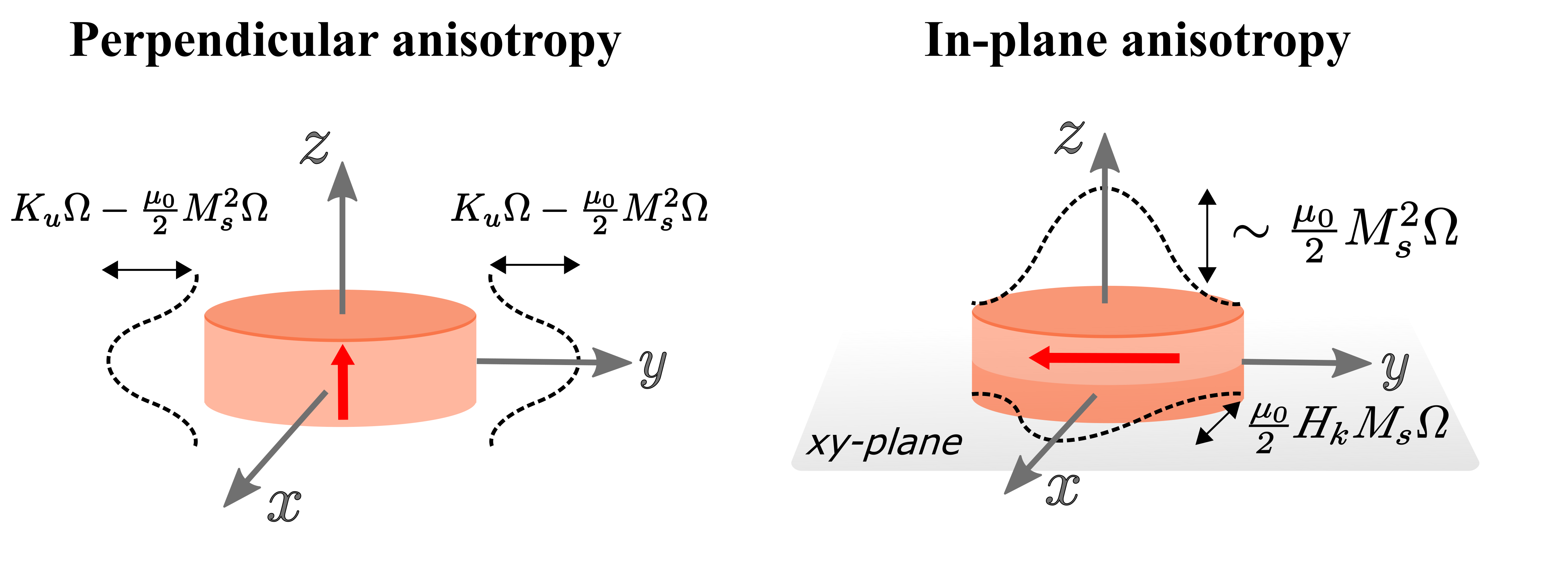
In PMA magnets, due to the lack of the out-of-the-plane demagnetization field (see fig. 20 for a visualization), the minimum current is:
| (13) |
The difference can be substantial for magnets with large saturation magnetization values, such as . Reduction of the drive current without any reduction in the stability of the magnets is beneficial in reducing the total Joule dissipation of the drive circuitry.
Challenges: PMA magnets are rapidly becoming a platform of choice for MRAM industry due to their scalability. However, challenges with high write error and stalling of the initial angle remain for the PMA magnets driven with Spin-Transfer Torque (STT). Another critical challenge to the PMA magnet based MTJs is scaling up write current density with scaling down of bit size, which can be understood in the following way.
For a monodomain magnet, the expected thermal stability time is:
| (14) |
where usually. Using gives us a decade of state retention which is a typical design target for memory applications. Even if the magnet area scales down the write current is fixed for a fixed as evident from eq. 13. Therefore as the volume is reduced by scaling down the diameter , the current density increases . Considering that the resistance of MTJ junctions also increase with scaling down the cross section area, scaling poses reliability and longevity challenges of electro-migration and dielectric breakdown of the MgO oxide layer.
7.2 Giant Spin-Hall Effect
Physics: It is well known that materials with Spin-Orbit Coupling have internal magnetic fields dyakonov1971current that can give rise to intrinsic spin-polarization and spin-Hall effect sih2005spatial . It has also been demonstrated that the spin accumulation at the interface of a heavy metal (Pt, W, ) and a magnet (CoFeB) can reliably switch the magnetization of the magnet liu2011spin . This has been explained either through the mechanism of Dzyaloshinskii-Moria (DM) interaction miron2010current , or through the accumulation of spins at the interface, which can then act as a virtual ”spin-battery” from which it is easy to inject spins pai2012spin compared to semiconductor-metallic magnet interfaces due to better impedance matching in all metallic material system.
Benefits: The primary motivation for GSHE based switching is the spin-current gain that can be obtained through geometry. The GSHE is given as where are the spin-current and charge-current densities in the transverse and the longitudinal directions respectively. Given that the charge current flows through (see fig. 19a) the GSHE film interface through the cross-section and spin current flows into the magnet through the cross-section , the current ratios, or in other words effective polarization (for , spin flip length in GSHE), is given as:
| (15) |
which can be controlled by device design and it is possible to obtain a polarization which can be viewed as a ‘gain’ from an engineering perspective. This can be intuitively understood through constant depolarization-repolarization of itinerant electrons at the interface of the GSHEMagnet films, due to the large internal field generated by large Rashba effect in the GSHE material. This constant depolarization-repolarization allows a single electron to impart multiple units of spin-torques to the magnet, as opposed to a spin injected from a fixed polarizing layer in MTJ or spin-valves.
Challenges: GSHE materials however have a challenges that can limit their performance. Some of these are:
-
1.
Magnet scalability: as described above, the gain is due to the geometry of the GSHEMagnet structure. This imposes a limit to the scalability of the magnets that can be switched without sacrificing the gain. Reducing the length of the magnet reduces the gain whereas the concomitant reduction of the width of the GSHEMagnet film system increases the resistance of the whole structure, causing higher dissipation ( losses).
-
2.
GSHE scalability: The GSHE film thickness cannot be scaled down indefinitely. For films with (spin-flip length) the expression for gain is hong2016spin :
(16) For . This is explained by mixing of the opposite polarization of the spins on the top and the bottom of thin GSHE film surfaces (assuming the same θ for both) causing reduction in effective . In addition, it has been found empirically that in general materials with high tend to have high charge resistivity, which limits the materials that can be used for obtaining high GSHE without high losses.
-
3.
Spin-current Shunting: The equation (16) for spin current injected into the magnet assumes that the magnet fully absorbs the entire spin current incident on it, i.e. it is a perfect ground for the spin current. However, magnets have finite resistance and for the spin-torque current, it is limited by the Sharvin resistance. Some amount of spins is reflected back from the GSHEMagnet interface. The shunting conductance of the magnet is given by where is the interface/mixing conductivity. The GSHE spin shunting conductance is given by . These two shunting paths share the spin current generated by the GSHE, reducing the spin-injection efficieny into the magnet.
-
4.
Charge-current Shunting: The charge resistivity of typical GSHE materials (say -Ta) is higher compared to the typical magnet material (say CoFeB). Therefore, a lot of the lateral charge current flowing in the GSHE gets shunted through the magnet rather than flowing through the GSHE, thereby reducing the effective amount of charge current available for spin-current generation.
7.3 Voltage-Controlled Magnetic Anisotropy
Physics: It has been demonstrated wang2012electric ; shiota2012induction ; kanai2014magnetization that it is possible to modulate the surface anisotropy of ultra-thin PMA magnets by application of an electric field (fig. 19b). This is caused primarily due to the reduction of the anisotropy field strength . Therefore, with this effect, it is possible to dynamically lower the energy barrier of the magnet and thereby reduce the write current necessary to switch the magnet (eq. 13).
The VCMA effect is phenomenologically described by pertsev2013origin :
| (17) |
The microscopic origins of this effect has been explained through accumulation/depletion of carriers at the interface of the MagnetOxide system. Spin-selective screening effects gives rise to a field dependent surface spin texture that changes the surface magnetic properties VCMAmicroscopicDFT . The strength of the effect is commonly expressed in the units of . For a magnet of area of cross section and for an electric field strength of the reduction of the anisotropy energy is about at room temperature. Values in excess of have been reported wang2012electric .
Benefits: The primary benefit of the VCMA is in its ability to reduce the write current required to switch the magnet through the extra voltage bias on the magnet, which can almost be thought of as a gate voltage. Therefore, it is possible to dynamically control the magnet’s volatility.
Challenges: The following are the challenges that limit the VCMA effectiveness:
-
1.
Magnet scalability: Being a surface effect, VCMA is proportional to the area of cross section of the interface and scales down as the magnet volume is scaled.
-
2.
Speed of switching: VCMA effect works by reducing the of the magnet, but leaves the product untouched. This means that the total charge that needs to be provided to switch the magnet ( camsari2016ultrafast ) does not change. Which means that the write current, though lower, needs to be provided for a longer time for full switching, therefore decreasing the speed of switching and potentially increasing the write error rate.
7.4 Magneto-Electric Effect
Physics: Multiferroics are a class of materials where multiple ”ferro” phases coexist at the same time, and it is usually possible to manipulate one phase by controlling the other. Multiferroics are either single phase materials such as etc. or they can be built through heterostructures (composite multiferroics) where the two ferro-phases interact through another intermediate ferro-phase.
It has been found that a large number of single phase multiferroics with ferroelectric order exhibit anti-ferromagnetism wang2010multiferroic . However, in (BFO), there is an uncompensated residual ferromagnetic order present (due to DM interaction) that is coupled with the ferroelectric order at room temperature ederer2005weak . By controlling the ferroelectric order through an applied voltage bias it is possible to control the ferromagnetism of the ME material. This can then be used to generate an effective controllable magnetic field on an adjacent magnetic film mediated via exchange interaction borisov2005magnetoelectric .
It has been experimentally demonstrated wu2010reversible ; heron2014deterministic that full reversible switching of a magnetic film grown over on top of a BFO is possible purely through voltage application on the BFO layer.
Basic phenomenological relationship of multiferroic phenomena is given by the magneto-electric tensor:
| (18) |
Using the definition and , we can relate the total magnetic field generated by the ME material to the total electric polarization. Note that this ignores the inbuilt polarization, which in principle will add dynamics of its own. The switching then is due to this generated magnetic field given by:
| (19) |
where is the applied voltage, is the thickness of the ME film, and is the intrinsic polarization of the ME material. The ref heron2014deterministic found a strong field dependence on and reported maximum value of .
Benefits: ME based switching opens a pathway towards voltage based magnetization switching (e.g. see fig. 19c as a possible structure), which is compatible with the current CMOS-based technology. The biggest advantage provided by the ME-based switching is the potential reduction of charge needed to switch the magnet. It can be shown from angular momentum considerations that the total amount of charge needed to switch a magnet is assuming polarization of spins camsari2016ultrafast . Therefore, larger the , higher the amount of charge needed, thereby having higher dissipation. However, the ME based switching, being in effect a field-like switching mechanism, needs to only provide sufficient amount of charge necessary to create the anisotropy field needed for switching the magnet which in principle can be much smaller and can be engineered by using a thin ME film ganguly2017evaluating .
Challenges: Some of the fundamental challenges with ME based switching are:
-
1.
Scalability of the ME material: This effect was demonstrated on BFO films that were substantially thick. The “gain” in this switching mechanism is due to the factor, which in theory can be very large for small , enabling a small voltage to switch a high magnet. However, it is not understood if it is possible to scale down the ME material while keeping the ME effect () large.
-
2.
Scalability of the magnet: The principle of scaling of a magnet by reduction of the volume needs to be balanced by increasing the or to maintain a . For spin-torque-driven switching, it is beneficial to reduce the and increase . However, for field based switching it is beneficial to increase and reduce . However, while can be varied over a wide range of values by lithography and fabrication albrecht2013bit , is determined by material composition and cannot be controlled through lithography. Therefore, scaling of ME based devices may require using complex exchange-coupled magnetic stacks employed by the storage industry for modern hard disk drives.
-
3.
Switching dynamics poorly understood — potentially low speed and high write failure mechanism: The paper heron2014deterministic deduced that the switching of the magnet was due to a complicated two-step rotation of the DMI-generated field, likely due to a complex interaction of the DMI and exchange interactions. Therefore, detailed micromagnetic studies and experiments are necessary to establish the physics of the effect. If the switching is a two-step phenomenon, it is likely to be a slow mechanism with high write failures.
7.5 Exchange Coupled Magnets
Physics: Instead of using a single large magnet with large anisotropy, it is possible to use a stack of exchange coupled magnets (fig. 19d) where the total anisotropy adds up to provide a stable magnet. That is, the total magnetic barrier of the stack built of layers is given by:
| (20) |
However, it was shown that if the magnet is made of two asymmetric layers with unequal but opposing/complementary magnetization directions, it is possible to switch the magnet with a much lower amount of charge, and is equivalent to switching a magnet with anisotropy that is the difference of the anisotropy of the two layers, given by camsari2016ultrafast :
| (21) |
Benefits: The primary benefit that is derived from exchange coupled stacks is the reduction of the total charge needed to switch the overall stack’s magnetization, without sacrificing the thermal stability.
Challenges: While this technique is widely adopted in the storage industry in building magnetic bits of extremely small dimensions albrecht2013bit , it has as yet not been adopted in the STT-MRAM industry due to lithography and fabrication challenges of building such complex stacks.
8 Putting it all together: Integrated approach based on analytical models
- 1.
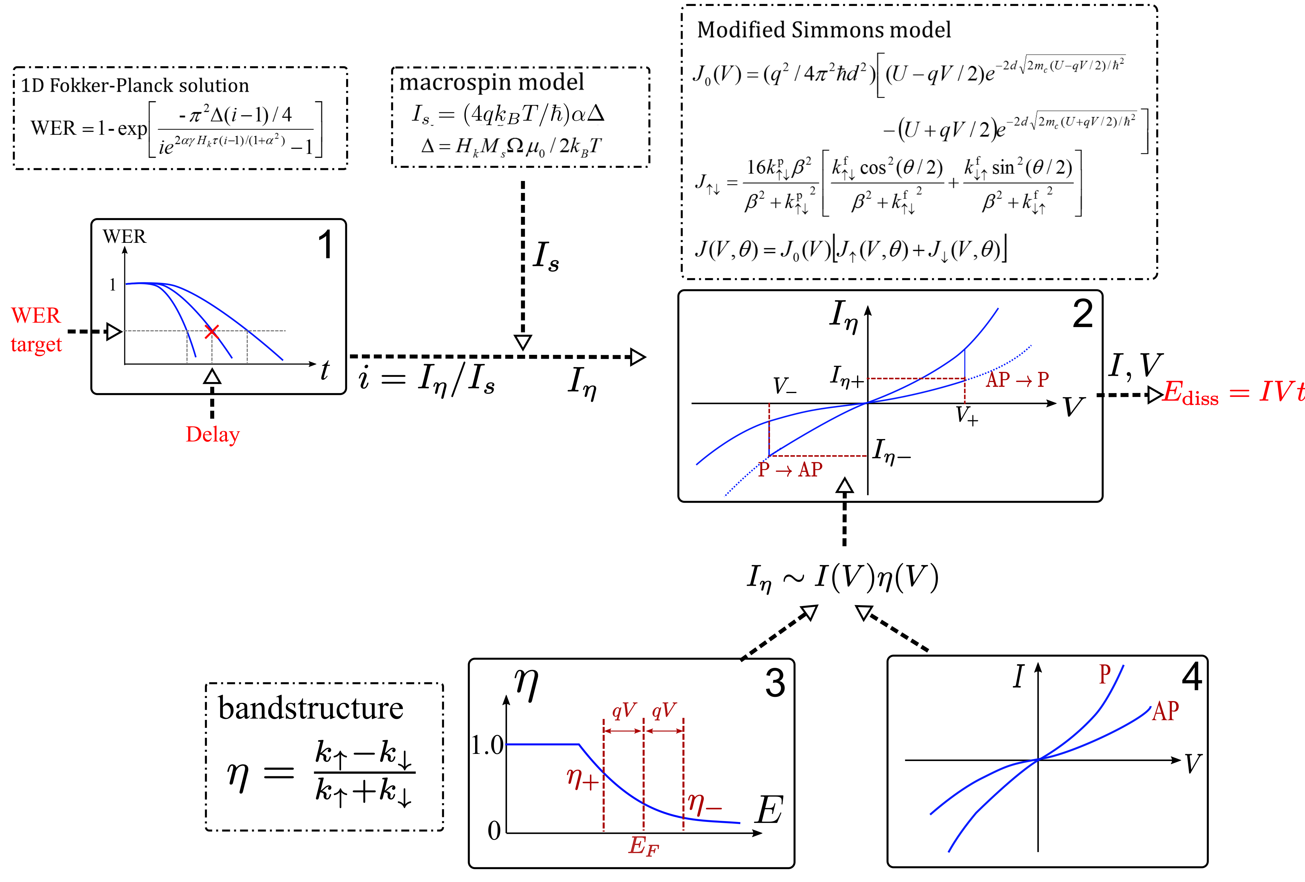
In this section, we use the magnetic tunnel junction as an example to show how to integrate different modules, each represented by an analytical compact model. Fig.21 shows the diagram and the underlying equations for this integrated approach to study the energy-delay-error of STT switchingmunira2012quasi . This process starts with a target write error rate and switching delay, which is usually application specific. The WER and are the input into an error model. Here we choose the analytical solution to the 1-D Fokker-Planck equation for WER in a perpendicular magnetic tunnel junction. In the 1D FPE model, WER is a function of switching delay and overdrive current as shown in the diagram. Instead of the usual way to express the overdrive current , we use the polarized current and critical current assuming spin polarization because the polarization factor is essential in determining the asymmetry in P-to-AP and AP-to-P switching and it is from the material properties independent of the macrospin error model. In the simplest case, one can just relate those quantities through and where is the polarization of the fixed magnet. Once the WER and are given, the equation solves for that matches the design target (an example of such a plot, obtained from numerical simulation of Fokker-Planck, was shown earlier in Fig.15). The second step is to translate the scaled into the polarized charge current . To do so, we need the intrinsic critical current assuming spin polarization, which we can solve under the macrospin assumptionSun2000 . Notice that these two modules have taken into account most of the magnetic properties of the free magnetic layer including the saturation magnetization, magneto-anisotropy and magnetic damping . To further evaluate the energy dissipation, a transport model is required to relate the polarized charge current to the voltage across the MTJ. While this needs a full NEGF simulation to capture the spin dependent electron tunneling, we use instead a simple transport model based on the modified Simmons equation derived in munira2012quasi . In that free electron model, the electronic structure of an MTJ can be described by the following six parameters: 1) the effective mass of the ferromagnetic layers ; 2) the effective mass of the nonmagnetic spacer ; 3) the Fermi energy to the bottom of the conduction band ; 4) the potential barrier height ; 5) the thickness of the nonmagnetic layer ; and 6) the band-splitting in the ferromagnetic layers due to the exchange energy . Under the free electron assumption, and are the spin dependent wavevectors in the pinned layer and the free layer respectively, is the tunneling parameter and is the angle between the magnetic moments of the pinned layer and the free layer. These six material parameters can be adjusted to fit the experimental TMR data at low-bias. Once fitted, they can simulate the entire I-V characteristics and spin transfer torque as well munira2012quasi . It also can be used to predict additional properties such as the spin torque switching voltages for example. The Simmons model incorporates the bandstructure from which the polarization factor can be extracted (Fig.21 Block 3). From the I-V (Fig. 21 Block 4) and , one can plot the , which combined with the input , can determine the switching point and switching voltage as shown in Fig. 21 (Block 2) where two ‘jump points’ indicate the switching between parallel and anti-parallel states. The final output from this process is the energy dissipation of STT switching in MTJs.
Even though each equation shown in diagram Fig.21 has its limitations, the idea of such integrated picture is more general and important. For MTJs, each block can be easily replaced by a more accurate and appropriate numerical model if needed. Some can even come from experimental measurements, which usually only focus on of those blocks. Putting those data in the context of other properties or requirements gives a clearer picture of where the technology stands. For other nanomagnetic applications, one can formulate the corresponding equations/models and build a similar process.
9 Towards System Level Simulations
9.1 Modular Approach to Spintronics
In the previous sections of this paper, we have demonstrated how the physics of charge and spin transport combined with magnetization dynamics of nanomagnetic materials can be modeled starting from ab-initio methods such as DFT. However, a multi-scale approach that can cater to an increasing number of materials and phenomena relevant for spintronics calls for the ability to create abstractions for ‘lower level’ physics based models and reuse those models and techniques for more complex designs built with multiple materials and phenomena, without losing the accurate behavior and properties captured by those models.
A recently developed Modular Approach to Spintronics camsari2015modular , based on the multi-component spin-circuit formalism, provides such a framework for multi-physics, multi-scale modeling, and simulation of spintronic and nanomagnetic devices. In essence, the approach is based on a set of carefully benchmarked elemental ”circuit modules” for transport physics and magnetodynamics and interaction through various materials. These models are then combined in a ‘lego-block’ fashion to build a larger circuit model for a complex experimental structure or functional device and then simulated in a standard circuit simulation software (SPICE). This approach was used to study the performance and dissipation in a large family of spintronic devices as well as explore novel non-Boolean computing schemes using stochastic magnetodynamics ganguly2017evaluating .
In a nutshell, the aim of this effort is to marry decades of development in complex circuit simulation techniques with fundamental atomistic methods surveyed in this paper. The Modular Approach to Spintronics is a multi-organization open source initiative with a large library of modules and illustrative example models that are available through its project portal modularwebsite .
A typical workflow utilizing the methods laid out in this paper will be:
-
1.
Materials Modeling (DFT): calculate stable candidate materials and their material properties such as anisotropy. Generate Hamiltonian matrices for the material for use in transport calculations.
-
2.
Transport Modeling (NEGF, Spin-Diffusion): Using the Hamiltonian generated from materials modeling, apply NEGF methods to calculate I-V and other transport characteristics (say torques, spin currents etc.)
-
3.
Compact Modeling: From the transport modeling results, develop analytical/semi-analytical equations relating charge and spin currents and voltages at the ‘terminals’ of the material.
-
4.
Device Modeling: Use the compact model developed before to create a circuit model for the test device, bringing together other modules previously developed, which can also include magnetodynamic modules (LLG).
-
5.
Circuit Modeling: Use the device model in a circuit testbench of choice and analyze performance. Use the results to define the targeted parameter space and go back to step 1 to search for ‘better’ materials.
9.2 Spin-based Logic
The emerging write mechanisms discussed above have created the possibility of building multi-terminal nanomagnetic devices where simultaneous read and write operations can be performed, unlike a two-terminal MTJ. As a result, a wide variety of spintronic logic devices have been proposed. The fundamental principle underlying most of these devices is the coupling of a write and a read unit datta_what_2014 , which may or may not be electrically isolated. Some of the spin-logic device proposals are:
-
•
All Spin Logic (ASL) behin-aein_proposal_2010 and its variants: Works on the principle of non-local spin-transfer torque, where two nano-magnets interact through non-local spin-currents. The variant designs attempt to improve the performance by using different materials for the spin-channels, PMA magnets, VCMA effect to assist in writing, etc.
-
•
Domain Wall based spin-logic devices (including m-Logic zhu_mlogic:_2015 ): Works on the principle of the controlled motion of a magnetic nanowire’s domain through spin-torque and read-out by an MTJ. It can be viewed as an ASL device using spin-waves instead of spin-currents.
-
•
Spin-Switch using Spin-Orbit torques datta_non-volatile_2012 : Using a GSHE driven magnet as a write unit and a complementary MTJ pair as a read unit, with both coupled by a magnetic interaction. In the rest of this section, we will show how to build circuit model for the Spin-Switch using the Modular Approach.
-
•
Magnetoelectric spin logic devices ganguly2017evaluating ; jaiswal2017mesl ; mankalale2016fast : Works by using the magnetoelectric effect as the writer for a spin logic device.
-
•
Strain-based devices dsouza_four-state_2011 : Works by using the piezzoelectric effect to manipulate the anisotropy of the nanomagnet and consequently reducing the write current in a spin-logic switch.
-
•
Nano-Magnetic Logic imre_majority_2006 : QCA like computing with nano-magnets interacting through magnetic fields rather than spin-currents.
9.3 Circuit Model for the Spin-Switch and Device Characteristics
The Spin-Switch datta_non-volatile_2012 is composed of a write unit, consisting of a GSHE-driven free nano-magnet, and a read unit, consisting of a complementary MTJ pair (APP) sharing a common free layer. The two free layers are coupled magnetically with an oxide layer that provides electrical isolation between the two units. This device has an internal gain from the GSHE based writer, which ensures that it is switched by the write magnet in preference to the read magnet since the MTJ pair’s spin-current does not have any gain, providing directivity of information flow from input to output. The electrical isolation allows the separation of biasing points among various stages in a circuit built from this device.
While the spin switch has all the required features for a logic device, its performance is not comparable to a CMOS inverter in terms of energy-delay product per switching event metrics nikonov_benchmarking_2015 due to inefficiencies associated with spin-torque switching. But it can be improved to a large extent by adopting various high-performance materials ganguly2017evaluating . Here we do not go into the details of the physics of the spin switch and various optimization possibilities. Instead, we want to show how to assemble a device model for the Spin-Switch (available from nanoHUB.org21 ) and explore its operations.
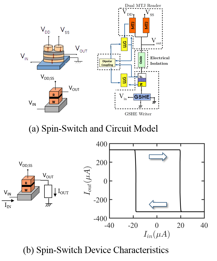
Fig. 22a shows the schematic design of the Spin-Switch on the top left and its compact representation at the bottom left. On the right, we show the circuit models based on the elemental modules for the transport and the magnetodynamics using the Modular Approach, e.g. the GSHE module encompasses the physics of the charge/spin transport through the GSHE material in the Spin-Switch design. The LLG module calculates the instantaneous time dependent magnetization of a nanomagnet with two inputs: the magnetic field and the injected spin current. The magnetization can then be fed into the magnet module and the MTJ module, as well as the magnetic interaction module (dipolar in this case), to calculate the total mutual magnetic field between the read and the write units.
The modules have been designed to maintain the validity of Kirchoff’s Laws of circuits by treating phenomena such as spin generation and decay as dependent sources and shunts, and the non-electrical quantities such as spin current, voltages, magnetic fields, and magnetizations as vector voltages and currents. The circuit model can, therefore, be connected with any other classic electrical elements like voltage and current sources, capacitors, resistors, transistors etc. and used in any SPICE-like circuit simulator to perform sophisticated simulations such as parametric and data-driven sweeps, noise, measure based metrology, rf and etc.
As an example, we use a simple testbench shown in fig. 22b. The input current is swept first from positive to negative values and then vice versa. The output current flowing through the load resistor is recorded. The device characteristics show hysteresis, as expected from a device with built-in memory from the magnets. It is clear that the swing of the output current is larger than the input current window, which indicates a gain in the device that enables it to drive multiple Spin-Switches at its output, i.e. fan out 1, and can be used to build logic pipelines without the need of amplifier or buffer stages. The output load was chosen to match the input impedance of another Spin-Switch (an arbitrary choice) and the Spin-Switch’s magnetic anisotropy barrier is set , which is not necessary for a logic device but has been chosen to demonstrate the built-in memory aspect of the device. The sweeps are performed in a time varying fashion, i.e. a transient analysis has been used instead of the dc sweep to accurately capture the magnetodynamics of the device. Thermal noise has been ignored for this simulation, i.e. the simulation is performed at .
9.4 Simulating Noise Margin and Signal Recovery in a Logic Pipeline
The Spin-Switch circuit model can be used to build larger circuits and analyze their performance through the circuit simulation. See gangulythesis for a comprehensive study of Energy-Delay of the Spin-Switch and its variant designs. In this section, we will use a FO-1 chain of inverters built from the Spin-Switch to study its noise margin and recovery.
A chain of 4 inverters built from identical Spin-Switches with a terminating load matching the input impedance has been setup as shown in fig. 23. Using transient noise simulation available in commercial SPICE simulators, it is possible to simulate the Langevin dynamics of the nanomagnets (Brownian motion). This is done by including a noise source in the LLG solver module and record the noisy output from the devices, consistent with how an experiment may be performed in a real life setup. It is then possible for a Monte Carlo simulation of the dynamics over many samples to obtain the statistical properties matching the real device performances.
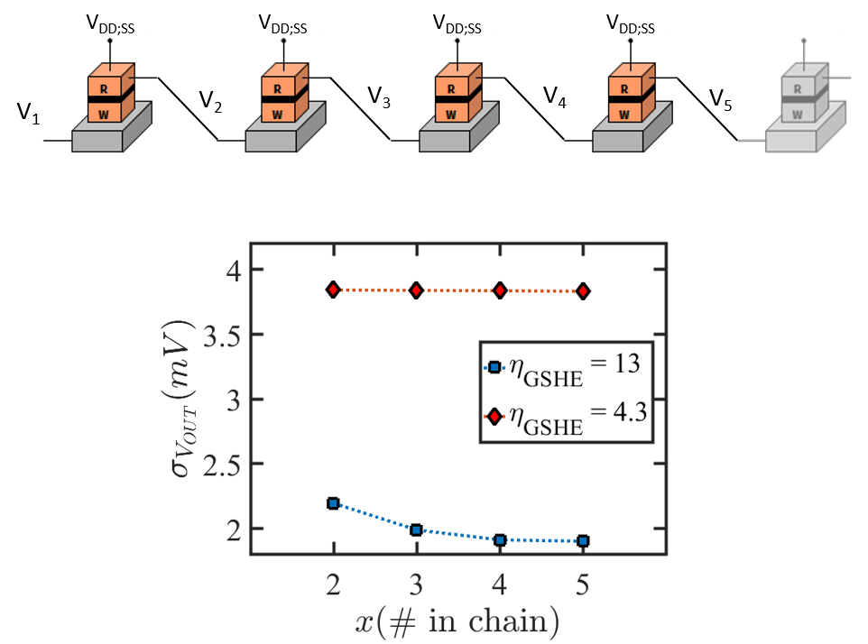
We perform a transient simulation for slowly rising input signal and record the switching points of each Spin-Switch in the chain (). From the multiple Monte Carlo samples, we calculate the standard deviation of the switching voltages for each device. This calculation is performed with two different GSHE gains.
It can be seen that for the device with a higher gain, the overall deviation is lower compared to the device with a lower gain, resulting in a tighter noise margin. This can be explained by the fact that higher gain helps boost the Signal-to-Noise ratio (noise being thermal in origin). Additionally, it can be seen that the deviation decreases further down the chain. This shows that the gain helps in recovery of a noisy input signal as it propagates through a logic pipeline, and higher the gain, better the recovery.
The point of this exercise is, firstly, to show a proof-of-concept complex simulation made available for spintronic devices due to the Modular Approach. Secondly, it demonstrates the principle of signal recovery through the in-built gain in a circuit composed of multiple Spin-Switches.
9.5 Probabilistic Spintronic Logic
A recent development in spintronic logic is to utilize the stochastic switching of nanomagnets for novel non-Boolean circuits and architectures. As noted earlier, the spin-torque based switching is inherently disadvantageous compared to MOSFETs in terms of Energy-Delay-Reliability product. Therefore it does not seem to be a viable alternative as a direct CMOS drop-in replacement in conventional circuits.
However, there are other possible applications where the inherent physics of spintronics and nano-magnets can enable new classes of devices with higher functional efficiency, i.e. to map a complex logic function directly into the hardware. There are two attractive features of spintronic/nanomagnetic devices: the natural addition of currents in metal interconnects of spin devices that enables the majority logic type functionality; the thresholding of magnetization switching that is attractive in building neuromorphic circuits diep_spin_2014 ; sharad_spin-neurons:_2013 ; ramasubramanian_spindle:_2014 . In addition, stochastic thermal switching of nanomagnets has opened the possibility of building networks that embrace the uncertainties for more energy efficient circuits ganguly2017evaluating ; us_department_of_commerce_stochastic_???? ; venkatesan_spintastic:_2015 ; locatelli_spintronic_2015 ; behin2016building ; PSLpaper ; faria2016low .
In the rest of this section, we illustrate the principles behind the spintronic stochastic switching and computation using a variant of the Spin-Switch design. For this example, we lower the anisotropy barrier of the nanomagnet in the Spin-Switch from to , which can be achieved with a superparamagnet. From eq. 14, the lower energy barrier reduces the device retention from a decade to a few ns. It can be shown ganguly2017evaluating ; sutton2016intrinsic that the statistical mean of the output voltage can be controlled by a spin-current, which produces a device characteristic that resembles a sigmoid function(see fig.24a. The blue background is the noisy instantaneous response as the input current is swept, while the red is a sampled mean produced through a network acting as a low pass filter.)
Connecting these devices together with controllable interaction through spin current allows us to form Restricted Boltzmann Machines (a class of stochastic recurrent neural networks) that can learn and reproduce patterns through annealing. The stochasticity of the superparamagnets is advantageous in scanning the phase space at GHz frequencies and reaching the ground state (solution state) quickly during the annealing process.
A proof-of-concept example of the annealing process is shown in fig. 24b, where a circuit built from 3 stochastic Spin-Switches forms a 3-node Ising network. The connections among them can be weighted by an external circuitry independent from the Spin-Switches. Some possible ways to implement the weighted connections are voltage controlled resistors such as memristors, bias voltages on the Spin-Switches themselves, or an external CMOS based circuitry borders2016analogue . In this example, the magnitudes of the weights are chosen to give strong connections that can drive the devices unambiguously into the saturation regions in fig.24a. When the signs of the connections are all positive, the interaction type is ferromagnetic and therefore after annealing, those devices prefer and states equally, with very low probability to choose other states. On the other hand, if the interactions are negative (anti-ferromagnetic) the networks settle into a frustrated spin-glass state (fig.24c).
With this type of network, it is possible to compute any logic function by adjusting the interactions to encode the desired answer or truth table into its eigenstates, which the network can find quickly through the annealing process. An example is to solve a Travelling Salesman Problem (a classic NP-complete problem) with an Ising network demonstrated in ref. sutton2016intrinsic . Another example is to implement a 32-bit Ripple Carry Adder with functional complementarity discussed in ref. PSLpaper .
The purpose of this section is to demonstrate the capabilities of the integrated DFT to SPICE approach presented in this paper that allows us to directly connect the physics of the materials to the performance of functional memory and logic devices as well as explore novel circuit applications enabled by these materials.
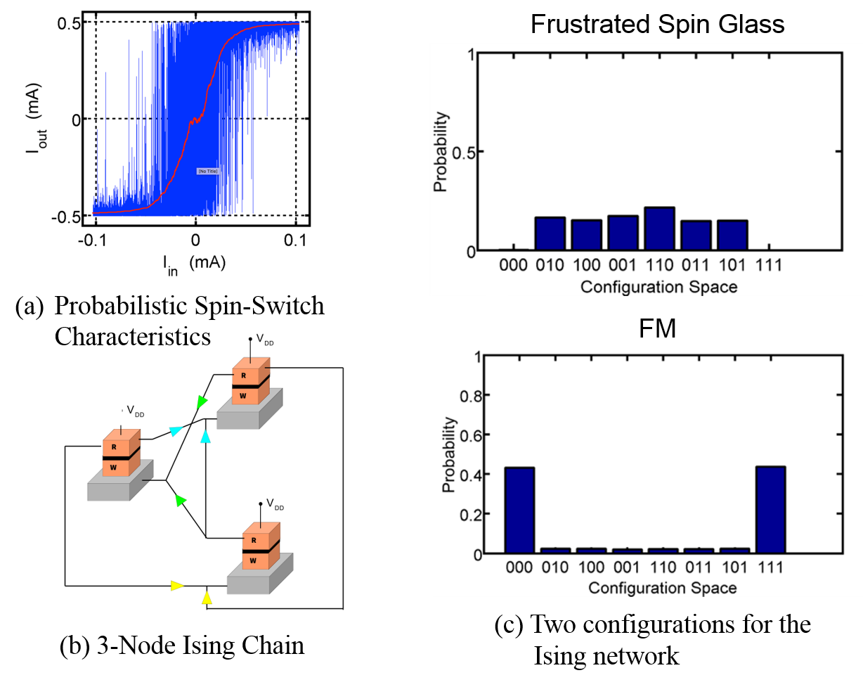
10 Summary
Traditional STT-MRAMs have already started commercializing to some extent. The continual improvement in the material engineering and fabrication process will promise better device performance in terms of the read-write-reliability metrics, which makes it a competitive candidate in memory applications. Following these efforts, we have summarized the computational tools that facilitate the material study and demonstrated a wide range of material choices in the Heusler family with the potential to improve the performance of MTJs at scaled nodes. We have also illustrated the importance of the thermal noise in magnetization switching and how to characterize its effect using the LLGS and Fokker-Planck methods. A proper engineering of the nanomagnet (such as tilted magnetic moment) can mitigate some negative effects from the thermal noise. However, the low power dissipation goal promised by nano-magnetics can hardly be achieved in conventional magnetic tunnel junction structure with spin transfer torque switching. On the one hand, emerging device ideas such as GSHE bring new hope toward energy efficient operations of nanomagnetic devices in traditional applications. On the other hand, a paradigm shift towards non-boolean computation might bring nanomagnetic into new application realms such as probabilistic computing, neuromorphic computing and etc. In any case, a comprehensive understanding of a nanomagnetic device - from its material to its circuit performance is necessary to be able to optimize it to meet the requirements of different applications. To do that, we have shown an integrated framework that connects the material properties to the circuit performance and illustrated it with different devices such as the STT-MRAM and the Spin-Switch. Each part of the toolbox is general enough to be extended to study other device ideas. We hope these tools can serve researchers from different communities and connect their expertise and advancement to inspire novel yet practical solutions.
Acknowledgment
We acknowledge discussions with Prof. W. H. Butler on Heusler studies, I. Rungger and S. Sanvito from the Smeagol team for ab-initio transport calculations, P. Visscher and B. Behin-Aein on Fokker-Planck and write error study in STT-MRAM. We also acknowledge the support from Oak Ridge National Laboratory (ORNL) center for nanophase materials sciences (CNMS) on computational resources. This work was funded over the years by NSF-DMREF-1235230, DARPA, NSF-SHF, SRC-NRI and IBM Fellowship.
References
- [1] Avik Ghosh. Nanoelectronics: A molecular view, 2016.
- [2] Sayeef Salahuddin and Supriyo Datta. Interacting systems for self-correcting low power switching. Applied physics letters, 90(9):093503, 2007.
- [3] Yiming Huai. Spin-transfer torque MRAM (STT-MRAM): Challenges and prospects. AAPPS Bulletin, 18.6:33–40, 2008.
- [4] Laura M Grupp, John D Davis, and Steven Swanson. The bleak future of nand flash memory. In Proceedings of the 10th USENIX conference on File and Storage Technologies, pages 2–2. USENIX Association, 2012.
- [5] Peter Clarke. Everspin samples 256mbit mrams, 1gbit coming.
- [6] GLOBALFOUNDRIES. Globalfoundries launches embedded mram on 22fdx platform.
- [7] David Manners. Everspin and glofo to put embedded mram on socs.
- [8] Tom Coughlin. Memories of the future.
- [9] Shinji Yuasa, Taro Nagahama, Akio Fukushima, Yoshishige Suzuki, and Koji Ando. Giant room-temperature magnetoresistance in single-crystal fe/mgo/fe magnetic tunnel junctions. Nature materials, 3(12):868–871, 2004.
- [10] Stuart SP Parkin, Christian Kaiser, Alex Panchula, Philip M Rice, Brian Hughes, Mahesh Samant, and See-Hun Yang. Giant tunnelling magnetoresistance at room temperature with mgo (100) tunnel barriers. Nature materials, 3(12):862–867, 2004.
- [11] S Ikeda, J Hayakawa, Y Ashizawa, YM Lee, K Miura, H Hasegawa, M Tsunoda, F Matsukura, and H Ohno. Tunnel magnetoresistance of 604% at 300 k by suppression of ta diffusion in co fe b/ mg o/ co fe b pseudo-spin-valves annealed at high temperature. Applied Physics Letters, 93(8):082508, 2008.
- [12] P Khalili Amiri, ZM Zeng, P Upadhyaya, G Rowlands, H Zhao, IN Krivorotov, J-P Wang, HW Jiang, JA Katine, J Langer, et al. Low write-energy magnetic tunnel junctions for high-speed spin-transfer-torque mram. IEEE Electron Device Letters, 32(1):57–59, 2011.
- [13] PG Mather, JC Read, and RA Buhrman. Disorder, defects, and band gaps in ultrathin (001) mgo tunnel barrier layers. Physical Review B, 73(20):205412, 2006.
- [14] Stuart SP Parkin, Masamitsu Hayashi, and Luc Thomas. Magnetic domain-wall racetrack memory. Science, 320(5873):190–194, 2008.
- [15] S Ikeda, K Miura, H Yamamoto, K Mizunuma, HD Gan, M Endo, Sl Kanai, J Hayakawa, F Matsukura, and H Ohno. A perpendicular-anisotropy cofeb–mgo magnetic tunnel junction. Nature materials, 9(9):721–724, 2010.
- [16] Masahiko Nakayama, Tadashi Kai, Naoharu Shimomura, Minoru Amano, Eiji Kitagawa, Toshihiko Nagase, Masatoshi Yoshikawa, Tatsuya Kishi, Sumio Ikegawa, and Hiroaki Yoda. Spin transfer switching in tb co fe/ co fe b/ mg o/ co fe b/ tb co fe magnetic tunnel junctions with perpendicular magnetic anisotropy. Journal of Applied Physics, 103(7):07A710, 2008.
- [17] T Maruyama, Y Shiota, T Nozaki, K Ohta, N Toda, M Mizuguchi, AA Tulapurkar, T Shinjo, M Shiraishi, S Mizukami, et al. Large voltage-induced magnetic anisotropy change in a few atomic layers of iron. Nature nanotechnology, 4(3):158–161, 2009.
- [18] T Nozaki, Y Shiota, M Shiraishi, T Shinjo, and Y Suzuki. Voltage-induced perpendicular magnetic anisotropy change in magnetic tunnel junctions. Applied Physics Letters, 96(2):022506, 2010.
- [19] Wei-Gang Wang, Mingen Li, Stephen Hageman, and CL Chien. Electric-field-assisted switching in magnetic tunnel junctions. Nature materials, 11(1):64–68, 2012.
- [20] F. Jonietz, S. Mulbauer, C. Pfleiderer, A. Neubauer, W. Munzer, A. Bauer, T. Adams, R. Georgii, P. Boni, R. A. Duine, K. Everschor, M. Garst, and A. Rosch. Spin Transfer Torques in MnSi. Science, (September):1648–1652, 2011.
- [21] Luqiao Liu, Takahiro Moriyama, DC Ralph, and RA Buhrman. Spin-torque ferromagnetic resonance induced by the spin hall effect. Physical review letters, 106(3):036601, 2011.
- [22] Luqiao Liu, Chi-feng Pai, Y Li, H W Tseng, D C Ralph, and R A Buhrman. Spin-Torque Switching with the Giant Spin Hall Effect of Tantalum. 336(May):555–559, 2012.
- [23] Chi-Feng Pai, Luqiao Liu, Y Li, HW Tseng, DC Ralph, and RA Buhrman. Spin transfer torque devices utilizing the giant spin hall effect of tungsten. Applied Physics Letters, 101(12):122404, 2012.
- [24] AR Mellnik, JS Lee, A Richardella, JL Grab, PJ Mintun, Mark H Fischer, Abolhassan Vaezi, Aurelien Manchon, E-A Kim, N Samarth, et al. Spin-transfer torque generated by a topological insulator. Nature, 511(7510):449–451, 2014.
- [25] KM Masum Habib, Redwan N Sajjad, and Avik W Ghosh. Chiral tunneling of topological states: Towards the efficient generation of spin current using spin-momentum locking. Physical review letters, 114(17):176801, 2015.
- [26] RO Cherifi, V Ivanovskaya, LC Phillips, A Zobelli, IC Infante, E Jacquet, V Garcia, S Fusil, PR Briddon, N Guiblin, et al. Electric-field control of magnetic order above room temperature. Nature materials, 13(4):345–351, 2014.
- [27] JT Heron, JL Bosse, Q He, Y Gao, M Trassin, L Ye, JD Clarkson, C Wang, Jian Liu, S Salahuddin, et al. Deterministic switching of ferromagnetism at room temperature using an electric field. Nature, 516(7531):370–373, 2014.
- [28] Noel D’Souza, Mohammad Salehi Fashami, Supriyo Bandyopadhyay, and Jayasimha Atulasimha. Experimental clocking of nanomagnets with strain for ultralow power boolean logic. Nano letters, 16(2):1069–1075, 2016.
- [29] Yunkun Xie, Ivan Rungger, Kamaram Munira, Maria Stamenova, Stefano Sanvito, and Avik W Ghosh. Spin transfer torque: A multiscale picture. Nanomagnetic and Spintronic Devices for Energy-Efficient Memory and Computing, page 91, 2016.
- [30] J S White, I Levatić, a a Omrani, N Egetenmeyer, K Prša, I Zivković, J L Gavilano, J Kohlbrecher, M Bartkowiak, H Berger, and H M Rønnow. Electric field control of the skyrmion lattice in Cu2OSeO3. Journal of physics. Condensed matter : an Institute of Physics journal, 24:432201, 2012.
- [31] I. Galanakis, P. H. Dederichs, and N. Papanikolaou. Origin and properties of the gap in the half-ferromagnetic heusler alloys. Phys. Rev. B, 66:134428, Oct 2002.
- [32] S. J. Youn and B. I. Min. Effects of the spin-orbit interaction in heusler compounds: Electronic structures and fermi surfaces of nimnsb and ptmnsb. Phys. Rev. B, 51:10436–10442, Apr 1995.
- [33] Janusz Toboła and Jacques Pierre. Electronic phase diagram of the xtz (x=fe, co, ni; t=ti, v, zr, nb, mn; z=sn, sb) semi-heusler compounds. Journal of Alloys and Compounds, 296(1-2):243 – 252, 2000.
- [34] Hem Chandra Kandpal, Claudia Felser, and Ram Seshadri. Covalent bonding and the nature of band gaps in some half-heusler compounds. Journal of Physics D: Applied Physics, 39(5):776, 2006.
- [35] I Galanakis, Ph Mavropoulos, and P H Dederichs. Electronic structure and slater-pauling behaviour in half-metallic heusler alloys calculated from first principles. Journal of Physics D: Applied Physics, 39(5):765, 2006.
- [36] William H Butler, Claudia KA Mewes, Chunsheng Liu, and Tianyi Xu. Rational design of half-metallic heterostructures. arXiv preprint arXiv:1103.3855, 2011.
- [37] Jianhua Ma, Vinay I. Hegde, Kamaram Munira, Yunkun Xie, Sahar Keshavarz, David T. Mildebrath, C. Wolverton, Avik W. Ghosh, and W. H. Butler. Computational investigation of half-heusler compounds for spintronics applications. Phys. Rev. B, 95:024411, Jan 2017.
- [38] J. C. Slater and G. F. Koster. Simplified lcao method for the periodic potential problem. Phys. Rev., 94:1498–1524, Jun 1954.
- [39] G. Kresse and J. Furthmüller. Efficiency of ab-initio total energy calculations for metals and semiconductors using a plane-wave basis set. Computational Materials Science, 6(1):15 – 50, 1996.
- [40] Scott Kirklin, James E Saal, Bryce Meredig, Alex Thompson, Jeff W Doak, Muratahan Aykol, Stephan Rühl, and Chris Wolverton. The open quantum materials database (oqmd): assessing the accuracy of dft formation energies. npj Computational Materials, 1:15010, 2015.
- [41] A. R. Akbarzadeh, V. Ozoliņš, and C. Wolverton. First-principles determination of multicomponent hydride phase diagrams: Application to the li-mg-n-h system. Advanced Materials, 19(20):3233–3239, 2007.
- [42] Scott Kirklin, Bryce Meredig, and Chris Wolverton. High-throughput computational screening of new li-ion battery anode materials. Advanced Energy Materials, 3(2):252–262, 2013.
- [43] K. E. H. M. Hanssen, P. E. Mijnarends, L. P. L. M. Rabou, and K. H. J. Buschow. Positron-annihilation study of the half-metallic ferromagnet nimnsb: Experiment. Phys. Rev. B, 42:1533–1540, Jul 1990.
- [44] Michiko Terada, Keizo Endo, Yūkō Fujita, and Ren’iti Kimura. Magnetic properties of clb compounds; covsb, cotisb and nitisb. Journal of the Physical Society of Japan, 32(1):91–94, 1972.
- [45] L Heyne, T Igarashi, T Kanomata, K-U Neumann, B Ouladdiaf, and K R A Ziebeck. Atomic and magnetic order in the weak ferromagnet covsb: is it a half-metallic ferromagnet? Journal of Physics: Condensed Matter, 17(33):4991, 2005.
- [46] WH Butler, X-G Zhang, TC Schulthess, and JM MacLaren. Spin-dependent tunneling conductance of fe— mgo— fe sandwiches. Physical Review B, 63(5):054416, 2001.
- [47] Javad G. Azadani, Kamaram Munira, Jonathon Romero, Jianhua Ma, Chockalingam Sivakumar, Avik W. Ghosh, and William H. Butler. Anisotropy in layered half-metallic heusler alloy superlattices. Journal of Applied Physics, 119(4):043904, 2016.
- [48] Supriyo Datta. Quantum transport: atom to transistor. Cambridge University Press, 2005.
- [49] A Reily Rocha, Víctor M García-Suárez, S Bailey, C Lambert, J Ferrer, and S Sanvito. Spin and molecular electronics in atomically generated orbital landscapes. Physical Review B, 73(8):085414, 2006.
- [50] Ioannis Theodonis, Nicholas Kioussis, Alan Kalitsov, Mairbek Chshiev, and WH Butler. Anomalous bias dependence of spin torque in magnetic tunnel junctions. Physical review letters, 97(23):237205, 2006.
- [51] José M Soler, Emilio Artacho, Julian D Gale, Alberto García, Javier Junquera, Pablo Ordejón, and Daniel Sánchez-Portal. The siesta method for ab initio order-n materials simulation. Journal of Physics: Condensed Matter, 14(11):2745, 2002.
- [52] Ahmet Ali Yanik, Gerhard Klimeck, and Supriyo Datta. Quantum transport with spin dephasing: A nonequlibrium Green’s function approach. Physical Review B - Condensed Matter and Materials Physics, 76(4):1–11, 2007.
- [53] Xiao-Liang Qi and Shou-Cheng Zhang. Topological insulators and superconductors. Reviews of Modern Physics, 83(4):1057, 2011.
- [54] Behtash Behin-Aein, Deepanjan Datta, Sayeef Salahuddin, and Supriyo Datta. Proposal for an all-spin logic device with built-in memory. Nat Nano, 5(4):266–270, April 2010.
- [55] William Fuller Brown Jr. Thermal fluctuations of a single-domain particle. Physical Review, 130(5):1677, 1963.
- [56] WH Butler, Tim Mewes, Claudia KA Mewes, PB Visscher, William H Rippard, Stephen E Russek, and Ranko Heindl. Switching distributions for perpendicular spin-torque devices within the macrospin approximation. IEEE Transactions on Magnetics, 48(12):4684–4700, 2012.
- [57] Yunkun Xie, Behtash Behin-Aein, and Avik W Ghosh. Fokker—planck study of parameter dependence on write error slope in spin-torque switching. IEEE Transactions on Electron Devices, 64(1):319–324, 2017.
- [58] H Liu, D Bedau, JZ Sun, Stéphane Mangin, EE Fullerton, JA Katine, and AD Kent. Dynamics of spin torque switching in all-perpendicular spin valve nanopillars. Journal of Magnetism and Magnetic Materials, 358:233–258, 2014.
- [59] Huanlong Liu, Daniel Bedau, Dirk Backes, JA Katine, Jürgen Langer, and AD Kent. Ultrafast switching in magnetic tunnel junction based orthogonal spin transfer devices. Applied Physics Letters, 97(24):242510, 2010.
- [60] Justin M Shaw, Hans T Nembach, Mathias Weiler, TJ Silva, Martin Schoen, Jonathan Z Sun, and Daniel C Worledge. Perpendicular magnetic anisotropy and easy cone state in ta/co 60 fe 20 b 20/mgo. IEEE Magnetics Letters, 6:1–4, 2015.
- [61] JZ Sun, RP Robertazzi, J Nowak, PL Trouilloud, G Hu, DW Abraham, MC Gaidis, SL Brown, EJ O’Sullivan, WJ Gallagher, et al. Effect of subvolume excitation and spin-torque efficiency on magnetic switching. Physical Review B, 84(6):064413, 2011.
- [62] G Finocchio, B Azzerboni, GD Fuchs, RA Buhrman, and L Torres. Micromagnetic modeling of magnetization switching driven by spin-polarized current in magnetic tunnel junctions. Journal of applied physics, 101(6):063914, 2007.
- [63] Kamaram Munira and PB Visscher. Calculation of energy-barrier lowering by incoherent switching in spin-transfer torque magnetoresistive random-access memory. Journal of Applied Physics, 117(17):17B710, 2015.
- [64] MT Johnson, PJH Bloemen, FJA Den Broeder, and JJ De Vries. Magnetic anisotropy in metallic multilayers. Reports on Progress in Physics, 59(11):1409, 1996.
- [65] J. Sun. Spin-current interaction with a monodomain magnetic body: A model study. Physical Review B, 62(1):570–578, 2000.
- [66] MI Dyakonov and VI Perel. Current-induced spin orientation of electrons in semiconductors. Physics Letters A, 35(6):459–460, 1971.
- [67] Vanessa Sih, RC Myers, YK Kato, WH Lau, AC Gossard, and DD Awschalom. Spatial imaging of the spin hall effect and current-induced polarization in two-dimensional electron gases. Nature Physics, 1(1):31–35, 2005.
- [68] Ioan Mihai Miron, Gilles Gaudin, Stéphane Auffret, Bernard Rodmacq, Alain Schuhl, Stefania Pizzini, Jan Vogel, and Pietro Gambardella. Current-driven spin torque induced by the rashba effect in a ferromagnetic metal layer. Nature materials, 9(3):230–234, 2010.
- [69] Seokmin Hong, Shehrin Sayed, and Supriyo Datta. Spin circuit model for 2d channels with spin-orbit coupling. Scientific reports, 6, 2016.
- [70] Yoichi Shiota, Takayuki Nozaki, Frédéric Bonell, Shinichi Murakami, Teruya Shinjo, and Yoshishige Suzuki. Induction of coherent magnetization switching in a few atomic layers of feco using voltage pulses. Nature materials, 11(1):39–43, 2012.
- [71] S Kanai, Y Nakatani, M Yamanouchi, S Ikeda, H Sato, F Matsukura, and H Ohno. Magnetization switching in a cofeb/mgo magnetic tunnel junction by combining spin-transfer torque and electric field-effect. Applied Physics Letters, 104(21):212406, 2014.
- [72] Nikolay A Pertsev. Origin of easy magnetization switching in magnetic tunnel junctions with voltage-controlled interfacial anisotropy. Scientific reports, 3:2757, 2013.
- [73] Chun-Gang Duan, Julian P. Velev, R. F. Sabirianov, Ziqiang Zhu, Junhao Chu, S. S. Jaswal, and E. Y. Tsymbal. Surface magnetoelectric effect in ferromagnetic metal films. Phys. Rev. Lett., 101:137201, Sep 2008.
- [74] K. Y. Camsari, A. Z. Pervaiz, R. Faria, E. E. Marinero, and S. Datta. Ultrafast spin-transfer-torque switching of synthetic ferrimagnets. IEEE Magnetics Letters, 7:1–5, 2016.
- [75] Min Wang, Guo-Long Tan, and Qingjie Zhang. Multiferroic properties of nanocrystalline pbtio3 ceramics. Journal of the American Ceramic Society, 93(8):2151–2154, 2010.
- [76] Claude Ederer and Nicola A Spaldin. Weak ferromagnetism and magnetoelectric coupling in bismuth ferrite. Physical Review B, 71(6):060401, 2005.
- [77] Pavel Borisov, Andreas Hochstrat, Xi Chen, Wolfgang Kleemann, and Christian Binek. Magnetoelectric switching of exchange bias. Physical Review Letters, 94(11):117203, 2005.
- [78] SM Wu, Shane A Cybart, P Yu, MD Rossell, JX Zhang, R Ramesh, and RC Dynes. Reversible electric control of exchange bias in a multiferroic field-effect device. Nature materials, 9(9):756–761, 2010.
- [79] S. Ganguly, K. Y. Camsari, and S. Datta. Evaluating spintronic devices using the modular approach. IEEE Journal on Exploratory Solid-State Computational Devices and Circuits, 2:51–60, Dec 2016.
- [80] Thomas R Albrecht, Daniel Bedau, Elizabeth Dobisz, He Gao, Michael Grobis, Olav Hellwig, Dan Kercher, Jeffrey Lille, Ernesto Marinero, Kanaiyalal Patel, et al. Bit patterned media at 1 tdot/in 2 and beyond. IEEE Transactions on Magnetics, 49(2):773–778, 2013.
- [81] Kamaram Munira, William H Butler, and Avik W Ghosh. A quasi-analytical model for energy-delay-reliability tradeoff studies during write operations in a perpendicular stt-ram cell. IEEE Transactions on Electron Devices, 59(8):2221–2226, 2012.
- [82] Kerem Yunus Camsari. Modular approach to spintronics. 2015.
- [83] Group: Modular Approach to Spintronics.
- [84] Supriyo Datta, Vinh Quang Diep, and Behtash Behin-Aein. What constitutes a nanoswitch? A Perspective. arXiv:1404.2254 [cond-mat], April 2014. arXiv: 1404.2254.
- [85] J. G. J. Zhu, D. M. Bromberg, M. Moneck, V. Sokalski, and L. Pileggi. mLogic: All spin logic device and circuits. In 2015 Fourth Berkeley Symposium on Energy Efficient Electronic Systems (E3S), pages 1–2, October 2015.
- [86] Supriyo Datta, Sayeef Salahuddin, and Behtash Behin-Aein. Non-volatile spin switch for Boolean and non-Boolean logic. Applied Physics Letters, 101(25):252411, December 2012.
- [87] Akhilesh Jaiswal and Kaushik Roy. Mesl: Proposal for a non-volatile cascadable magneto-electric spin logic. Scientific Reports, 7, 2017.
- [88] Meghna G Mankalale, Zhaoxin Liang, Angeline Klemm Smith, DC Mahendra, Mahdi Jamali, Jian-Ping Wang, and Sachin S Sapatnekar. A fast magnetoelectric device based on current-driven domain wall propagation. In Device Research Conference (DRC), 2016 74th Annual, pages 1–2. IEEE, 2016.
- [89] Noel D’Souza, Jayasimha Atulasimha, and Supriyo Bandyopadhyay. Four-state nanomagnetic logic using multiferroics. J. Phys. D: Appl. Phys., 44(26):265001, 2011.
- [90] A. Imre, G. Csaba, L. Ji, A. Orlov, G. H. Bernstein, and W. Porod. Majority Logic Gate for Magnetic Quantum-Dot Cellular Automata. Science, 311(5758):205–208, January 2006.
- [91] D.E. Nikonov and I.A. Young. Benchmarking of Beyond-CMOS Exploratory Devices for Logic Integrated Circuits. IEEE Journal on Exploratory Solid-State Computational Devices and Circuits, 1:3–11, December 2015.
- [92] Samiran Ganguly, Kerem Yunus Camsari, and Supriyo Datta. Spin switch model, Oct 2014.
- [93] Samiran Ganguly. Spintronic Device Modeling and Evaluation Using Modular Approach to Spintronics. PhD thesis, Purdue University, December 2016.
- [94] Vinh Quang Diep, Brian Sutton, Behtash Behin-Aein, and Supriyo Datta. Spin switches for compact implementation of neuron and synapse. Applied Physics Letters, (22):222405, June.
- [95] Spin-neurons: A possible path to energy-efficient neuromorphic computers. Journal of Applied Physics, 114(23):234906, December 2013.
- [96] Shankar Ganesh Ramasubramanian, Rangharajan Venkatesan, Mrigank Sharad, Kaushik Roy, and Anand Raghunathan. SPINDLE: SPINtronic Deep Learning Engine for Large-scale Neuromorphic Computing. In Proceedings of the 2014 International Symposium on Low Power Electronics and Design, ISLPED ’14, pages 15–20, New York, NY, USA, 2014. ACM.
- [97] Alice Mizrahi, Nicholas Locatelli, Romain Lebrun, Vincent Cros, Akio Fukushima, Hitoshi Kubota, Shinji Yuasa, Damien Querlioz, and Julie Grollier. Controlling the phase locking of stochastic magnetic bits for ultra-low power computation. Scientific Reports, 6(30535), 2016.
- [98] R. Venkatesan, S. Venkataramani, X. Fong, K. Roy, and A. Raghunathan. Spintastic: Spin-based stochastic logic for energy-efficient computing. In 2015 Design, Automation Test in Europe Conference Exhibition (DATE), pages 1575–1578, March 2015.
- [99] Nicolas Locatelli, Adrien F. Vincent, Alice Mizrahi, Joseph S. Friedman, Damir Vodenicarevic, Joo-Von Kim, Jacques-Olivier Klein, Weisheng Zhao, Julie Grollier, and Damien Querlioz. Spintronic Devices As Key Elements for Energy-efficient Neuroinspired Architectures. In Proceedings of the 2015 Design, Automation & Test in Europe Conference & Exhibition, DATE ’15, pages 994–999, San Jose, CA, USA, 2015. EDA Consortium.
- [100] Behtash Behin-Aein, Vinh Diep, and Supriyo Datta. A building block for hardware belief networks. Scientific Reports, 6, 2016.
- [101] Kerem Yunus Camsari, Rafatul Faria, Brian M. Sutton, and Supriyo Datta. Stochastic p-bits for probabilistic spin logic. arXiv:1610.00377 [cond-mat.mes-hall], October 2016.
- [102] Rafatul Faria, Kerem Yunus Camsari, and Supriyo Datta. Low barrier nanomagnets as p-bits for spin logic. arXiv preprint arXiv:1611.05477, 2016.
- [103] Brian Sutton, Kerem Yunus Camsari, Behtash Behin-Aein, and Supriyo Datta. Intrinsic optimization using stochastic nanomagnets. arXiv preprint arXiv:1608.00679, 2016.
- [104] William A Borders, Hisanao Akima, Shunsuke Fukami, Satoshi Moriya, Shouta Kurihara, Yoshihiko Horio, Shigeo Sato, and Hideo Ohno. Analogue spin–orbit torque device for artificial-neural-network-based associative memory operation. Applied Physics Express, 10(1):013007, 2016.