Electronic Band Structure of Transition Metal Dichalcogenides from ab initio and Slater-Koster Tight-Binding Model
Abstract
Semiconducting transition metal dichalcogenides present a complex electronic band structure with a rich orbital contribution to their valence and conduction bands. The possibility to consider the electronic states from a tight-binding model is highly useful for the calculation of many physical properties, for which first principle calculations are more demanding in computational terms when having a large number of atoms. Here we present a set of Slater-Koster parameters for a tight-binding model that accurately reproduce the structure and the orbital character of the valence and conduction bands of single layer MX2, where Mo, W and S, Se. The fit of the analytical tight-binding Hamiltonian is done based on band structure from ab initio calculations. The model is used to calculate the optical conductivity of the different compounds from the Kubo formula.
I Introduction
Soon after the discovery of graphene by mechanical exfoliation, this technique was applied to the isolation of other families of van der Waals materials.Novoselov et al. (2005) Among them, semiconducting transition metal dichalcogenides (TMD) are of special interest because they have a gap in the optical range of the energy spectrum, what makes them candidates for applications in photonics and optoelectronics.Wang et al. (2012); Jariwala et al. (2014); Ganatra and Zhang (2014) The electronic properties of these materials are highly sensitive to the external conditions such as strain, pressure or temperature. For instance, a direct-to-indirect gap and even a semiconducting-to-metal transition can be induced under specific conditions.Feng et al. (2012); Pan and Zhang (2012); Peelaers and Van de Walle (2012); Scalise et al. (2014); Molina-Sánchez et al. (2015); Brumme et al. (2015) They also present a strong spin-orbit coupling (SOC) that, due to the absence of inversion symmetry in single layer samples, lifts the spin degeneracy of the energy bands.Zhu et al. (2011) In time reversal-symmetric situations, inequivalent valleys have opposite spin splitting, leading to the so called spin-valley coupling,Xiao et al. (2012); Xu et al. (2014); Babaee Touski et al. (2016) which has been observed experimentally.Zeng et al. (2012); Mak et al. (2012); Cao et al. (2012); Zeng et al. (2013); Wu et al. (2013); Wang et al. (2013) The coupling of the spin and valley degrees of freedom in semiconducting TMDs opens the possibility to manipulate them for future applications in spintronics and valleytronics nano-devices.Mak et al. (2013); Sallen et al. (2012); Zeng et al. (2012); Kormányos et al. (2014, 2015)
On the other hand, TMDs present a high stretchability. Moreover, external strain can be used to efficiently manipulate their electronic and optical properties.Roldán et al. (2015) Non-uniform strain profiles can be used to create funnels of excitons, that allows to capture a broad light spectrum, concentrating carriers in specific regions of the samples.Feng et al. (2012); San-Jose et al. (2016) Strain engineering can be also used to exploit the piezoelectric properties of atomically thin layers of TMDs, converting mechanical to electrical energy. Wu et al. (2014)
The rich orbital structure of the valence and conduction bands of semiconducting TMDsRoldán et al. (2014) complicates the construction of a tight-binding (TB) model for these systems. Such a TB model must be precise enough as to include all the pertinent orbitals of the relevant bands, but at the same time, simple enough as to be used without too much effort in calculations of optical and transport properties of these materials. The advantage of a tight-binding description with respect to first-principles methods is that it provides a simple starting point for the further inclusion of many-body electron-electron interaction, external strains, as well as of the dynamical effects of the electron-lattice interaction. Tight-binding approaches are often more convenient than ab initio methods for investigating systems involving a very large number of atoms,San-Jose et al. (2016) disordered and inhomogeneous samples,Yuan et al. (2014) strained and/or bent samples,Rostami et al. (2015); Pearce and Burkard (2015) materials nanostructured in large scales (nanoribbons,Rostami et al. (2015); Farmanbar et al. (2016) ripplesCastellanos-Gomez et al. (2013)) or in twisted multilayer materials. The aim of the present paper is twofold. Starting from the TB model for MoS2 developed by Cappelluti et al.,Cappelluti et al. (2013) we present a more accurate set of Slater-Koster parameters obtained from a more sophisticated fitting procedure, and we further generalize it to the other families of semiconducting TMDs, namely WS2, MoSe2 and WSe2. Finally, we apply the obtained tight-binding models to calculate the optical conductivity of the four compounds.
II Electronic Band Structure
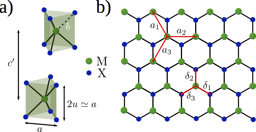
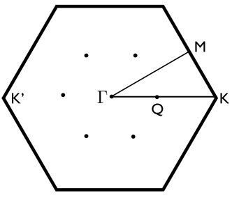
The crystal structure of MX2 is schematically shown in Fig. 1. A single layer is composed by an inner layer of metal atoms ordered on a triangular lattice, which is sandwiched between two layers of chalcogen atoms placed on the triangular lattice of alternating hollow sites. We use a notation such that corresponds to the distance between nearest neighbor in-plane and atoms, is the nearest neighbor separation and is the distance between the and planes. The MX2 crystal forms an almost perfect trigonal prism structure with and . The lattice parameters of the bulk compounds corresponding to the more commonly studied TMDs are given in Table 1.Liu et al. (2013); Kośmider et al. (2013); Kumar and Ahluwalia (2012) The in-plane Brillouin zone is an hexagon, and it is shown in Fig. 2. It contains the high-symmetry points , K and M. The six Q points correspond to the approximate position of a local minimum of the conduction band.
| MoS2 | |||
|---|---|---|---|
| MoSe2 | |||
| WS2 | |||
| WSe2 |
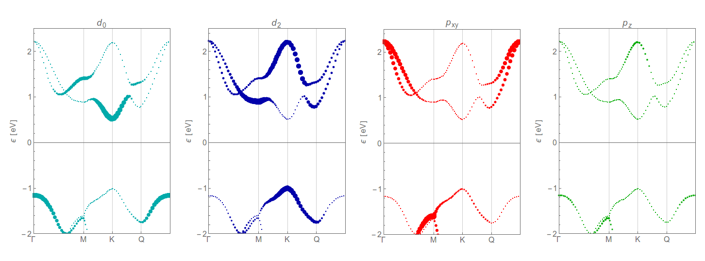
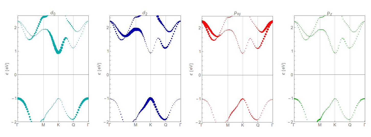
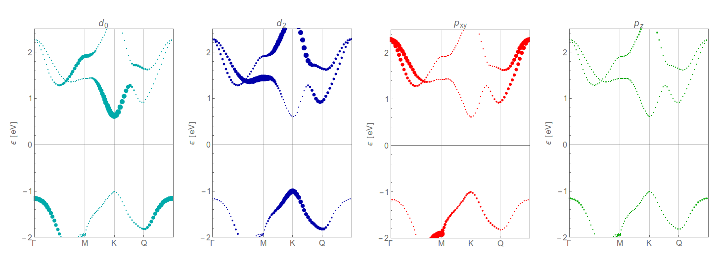
In order to study the electronic band structure of single-layer TMDs, we use the Density Functional Theory (DFT) calculations presented by some of the authors in Ref. Roldán et al., 2014, in which the intrinsic spin-orbit interaction term for all atoms is included. Fig. 3 shows the band structures for single-layer (black lines) together with the TB bands that will be discussed later (red lines).111DFT calculations were done using the Siesta code,SS02; AS08 with the exchange-correlation potential of Ceperly-AlderCA80 as parametrized by Perdew and Zunger.PZ81 A split-valence double- basis set including polarization functions was considered.AS99 The energy cutoff and the BZ sampling were chosen to converge the total energy with a value of 300 Ry and . The energy cutoff was set to eV. Spin-orbit interaction of the different compounds was considered by following the method developed in Ref. FF06. The lattice parameters used in the calculation are given in Table 1. One of the main characteristics of TMDs is that, contrary to what happens in other 2D crystals like graphene or phosphorene, the valence and conduction bands of present a very rich orbital contribution. As explained in detail in Ref. Cappelluti et al., 2013, they are made by hybridization of the orbitals of the transition metal, and the orbitals of the chalcogen. More specifically, the analysis of the orbital content of the set of bands containing the first four conduction bands and the first seven valence bands, which cover an energy window from -7 to 5 eV around the Fermi level, approximately, reveals that these bands are dominated by the five 4 (5) orbitals of the metal Mo (W) and the six (three for each layer) 3 (4) orbitals of the chalcogen S (Se), summing up to the % of the total orbital weight.Cappelluti et al. (2013)
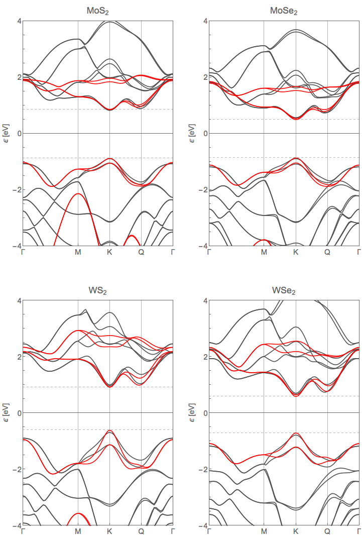
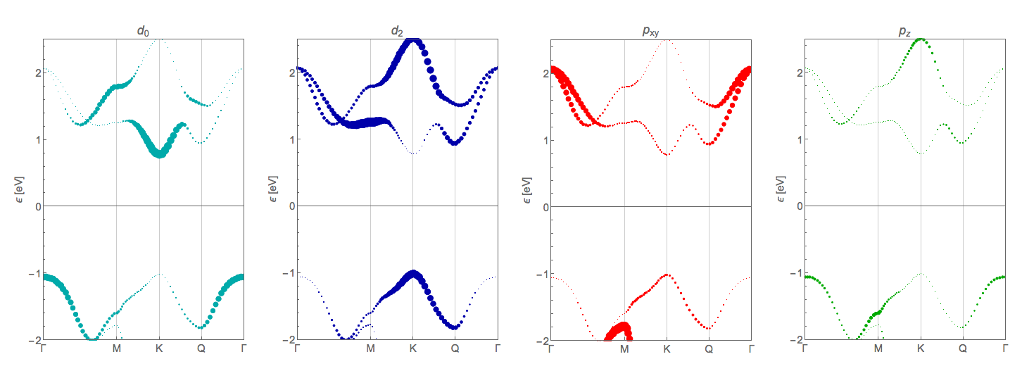
Single-layer TMDs are direct gap semiconductors, with the gap located at the two inequivalent K and K’ points of the Brillouin zone (Fig. 3). The main orbital character at the edge of the valence band is due to a combination of and orbitals of the metal , which hybridize with and orbitals of the chalcogen . On the other hand, the edge of the conduction band is formed by orbital of , plus some contribution of and orbitals of .Cappelluti et al. (2013) Contrary to single-layer samples, multi-layer compounds are indirect gap semiconductors. The edge of the valence band lies at the point of the BZ, having a major contribution from and orbitals of and atoms, respectively. The edge of the conduction band in multi-layer samples is placed at the Q point of the BZ. It is important to notice that the Q point is not a high symmetry point of the Brillouin zone, and therefore its exact position depends on the number of layers and on the specific compound. The orbital character at the Q point originates mainly from the and orbitals of the metal , plus and orbitals of the chalcogen , plus a non negligible contribution of and of and atoms, respectively. Figs. 4-8 represent these relative orbital weights in detail for the different compounds. The extremely rich orbital contribution to the relevant bands that occur in semiconducting TMDs complicates the derivation of a minimal TB model, valid in the whole Brillouin zone. Another important feature of TMDs is that they present a strong SOC, that leads to a large splitting of the valence band at the K and K’ points of the BZ (see Fig. 3). The splitting is bigger for W than for Mo compounds, due to the heavier mass of the former. SOC also leads to a splitting of the conduction band at the K point, as well as at the minimum at the Q point.Kośmider et al. (2013); Roldán et al. (2014)
III Tight-binding model
In this section we consider the electronic band structure of TMDs, in the whole BZ, from a Slater-Koster tight-binding approximation.Slater and Koster (1954) We use the model developed by Cappelluti et al.,Cappelluti et al. (2013) which contains 11 orbitals per layer. In particular, the model contains the five orbitals of the metal atom and the six orbitals of the two chalcogen atoms in the unit cell. The used scheme has been recently used in other works studying the electronic band structure of TMDs from a tight-binding perspective.Ridolfi et al. (2015); Fang et al. (2015) The corresponding base can be expressed asCappelluti et al. (2013)
| (1) |
where the indices and label the top and bottom chalcogen planes, respectively. The model is defined by the hopping integrals between the different orbitals, which are described in terms of , and ligands. In the following we reproduce the most important results, and we refer the reader to Refs. Cappelluti et al., 2013; Roldán et al., 2014 for details of the model. The Slater-Koster parameters that account for the relevant hopping processes of the model are and for bonds, , and for bonds, and and for bonds. Additional parameters of the theory are the crystal fields , , , , , describing respectively the atomic level of the (), the (, ), the (, ) orbitals, the in-plane (, ) orbitals and of the out-of-plane orbitals.
This model can be simplified by performing an unitary transformation that takes the orbitals of the top and bottom layers of the atoms into their symmetric and antisymmetric combinations with respect to the -axis. This way the 11-bands model is decoupled into a block with even (odd) symmetry of the () orbitals with respect to inversion, and a bands block with opposite combination. Since low energy excitations belong exclusively to the first block, the fit to DFT that we will present later will be performed within this sector. Therefore the relevant bands above and below the gap are well accounted by the reduced Hilbert space:
| (2) |
where the S and A superscripts stand for the symmetric and antisymmetric combinations of the p-orbitals of the atom, and , with . The tight-binding Hamiltonian defined by the base (2), including local spin-orbit coupling, can be expressed in real space as
| (3) |
where creates (annihilates) an electron in the unit cell in the atomic orbital , belonging to the Hilbert space defined by (2). The Hamiltonian in -space can be expressed as: Cappelluti et al. (2013); Roldán et al. (2014); Rostami et al. (2015)
| (4) |
where the vectors () and () are shown in Fig. 1(c). The analytical expressions for the TB model are given in Appendix A.
| MoS2 | MoSe2 | WS2 | WSe2 | ||||
|---|---|---|---|---|---|---|---|
| SOC | 0.086 | 0.089 | 0.271 | 0.251 | |||
| 0.052 | 0.256 | 0.057 | 0.439 | ||||
| Crystal Fields | -1.094 | -1.144 | -1.155 | -0.935 | |||
| -0.050 | -0.250 | -0.650 | -1.250 | ||||
| -1.511 | -1.488 | -2.279 | -2.321 | ||||
| -3.559 | -4.931 | -3.864 | -5.629 | ||||
| -6.886 | -7.503 | -7.327 | -6.759 | ||||
| - | 3.689 | 3.728 | 7.911 | 5.803 | |||
| -1.241 | -1.222 | -1.220 | -1.081 | ||||
| - | -0.895 | -0.823 | -1.328 | -1.129 | |||
| 0.252 | 0.215 | 0.121 | 0.094 | ||||
| 0.228 | 0.192 | 0.442 | 0.317 | ||||
| - | 1.225 | 1.256 | 1.178 | 1.530 | |||
| -0.467 | -0.205 | -0.273 | -0.123 |
| Kv | Kc | ||||||
|---|---|---|---|---|---|---|---|
| DFT | TB | DFT | TB | DFT | TB | ||
| MoS2 | 0.0 | 0.0 | 0.82 | 0.77 | 0.66 | 0.96 | |
| 0.76 | 1.0 | 0.0 | 0.0 | 0.0 | 0.0 | ||
| 0.20 | 0.0 | 0.12 | 0.23 | 0.0 | 0.0 | ||
| 0.0 | 0.0 | 0.0 | 0.00 | 0.28 | 0.04 | ||
| MoSe2 | 0.0 | 0.0 | 0.83 | 0.83 | 0.71 | 0.96 | |
| 0.78 | 1.0 | 0.0 | 0.0 | 0.0 | 0.0 | ||
| 0.18 | 0.0 | 0.10 | 0.17 | 0.0 | 0.0 | ||
| 0.0 | 0.0 | 0.0 | 0.0 | 0.23 | 0.04 | ||
| WS2 | 0.0 | 0.0 | 0.80 | 0.76 | 0.64 | 0.98 | |
| 0.74 | 0.94 | 0.0 | 0.0 | 0.0 | 0.0 | ||
| 0.21 | 0.06 | 0.07 | 0.24 | 0.0 | 0.0 | ||
| 0.0 | 0.0 | 0.0 | 0.0 | 0.28 | 0.02 | ||
| WSe2 | 0.0 | 0.0 | 0.82 | 0.86 | 0.69 | 0.99 | |
| 0.73 | 0.95 | 0.0 | 0.0 | 0.0 | 0.0 | ||
| 0.20 | 0.05 | 0.05 | 0.14 | 0.0 | 0.0 | ||
| 0.0 | 0.0 | 0.0 | 0.0 | 0.23 | 0.01 | ||
IV Slater-Koster parameters from fitting to ab initio calculations
Finding the optimal set of Slater-Koster parameters for the TB model considered here is a difficult task. Two main requirements must be satisfied: a good reproduction of the structure of the relevant electronic bands, and faithful representation of the orbital contribution along such bands. The last condition is especially relevant because, for example, different kinds of strain do not affect all the hoppings in the same manner. Therefore capturing the proper orbital contribution is essential when using the TB model for calculations of physical properties of strained membranes. The same happens when one consider the effect of vacancies, adatoms, etc.
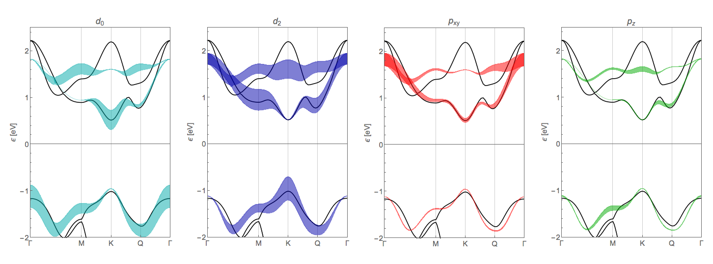
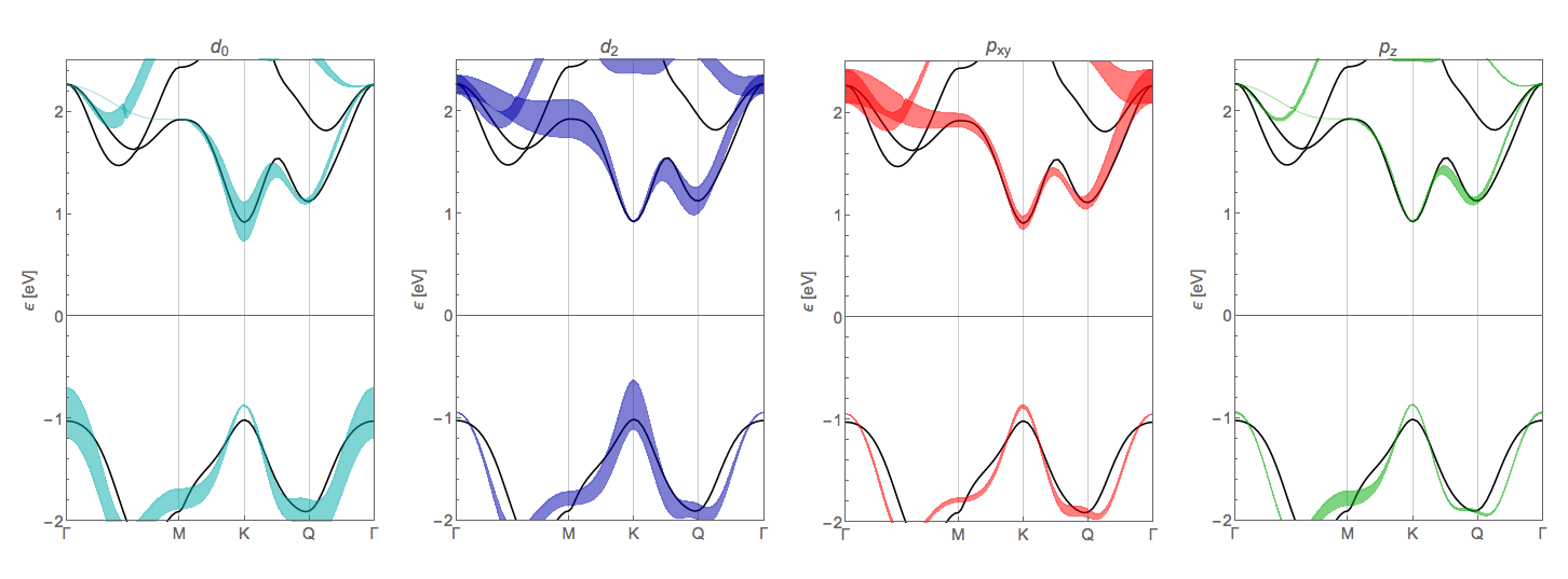
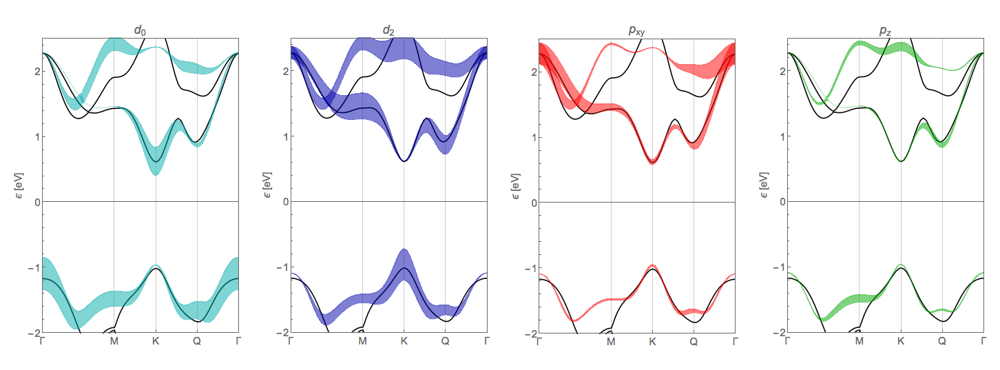
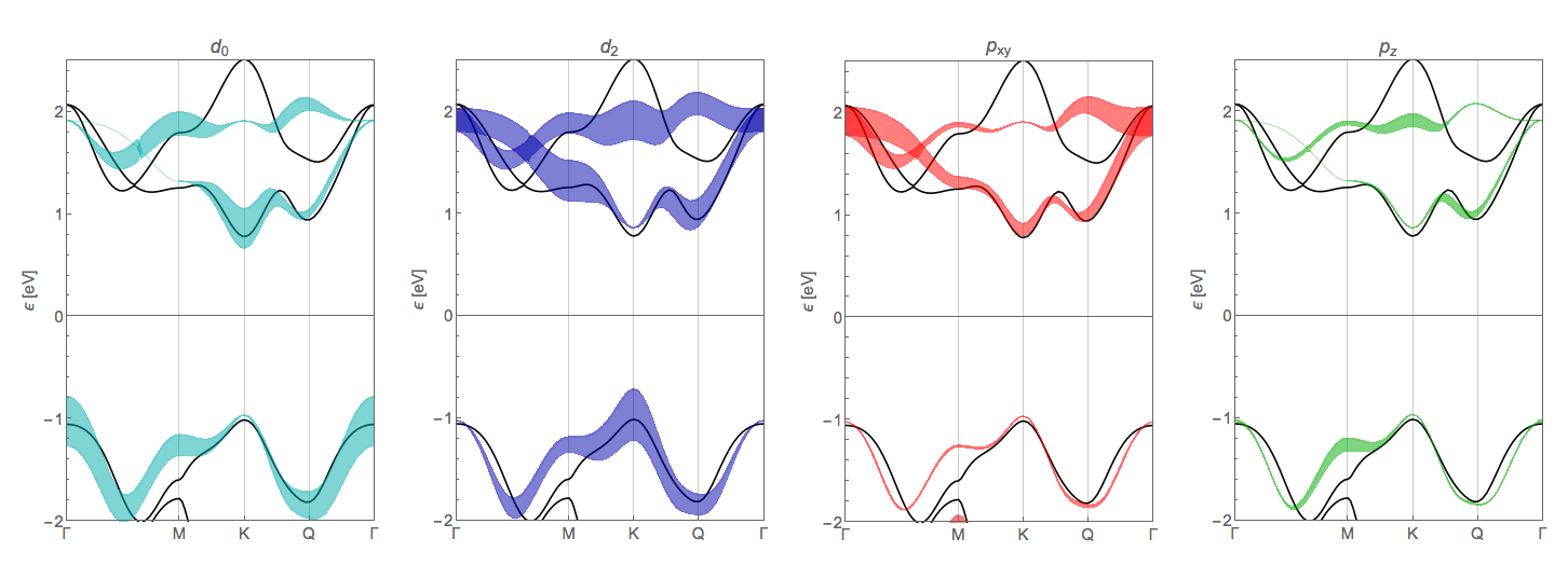
In this work we have obtained the Slater-Koster parameters for each compound from a minimization procedure which has the possibility to consider a band/momentum resolved weight, that allows us to resolve more accurately particular regions of selected bands (e.g. edges of the valence and conduction bands).222The calculation of tight-binding band structure and fitting to DFT have been performed using the MathQ package, developed by P. San-Jose. (Source: http://www.icmm.csic.es/sanjose/MathQ/MathQ.html). Furthermore, we can apply constrictions for the orbital contribution at specific band regions, taking as a reference the information from the DFT wave-functions. The sets of Slater-Koster parameters that we have obtained for the four compounds are given in Table 2. During the fitting we have used only the block of the Hamiltonian because, as explained above, it accounts for the valence and conduction bands. Therefore, we obtain as output all the Slater-Koster parameters but one, , which is the crystal field corresponding to orbitals, whose contribution is absent in the block. What we have done to estimate the value of is to impose that the edges of the TB and DFT bands coincide for the lower energy band of the block at the K point of the Brillouin zone. The band structure calculated with the block of this model is plotted in Fig. 3, as compared to DFT calculations. In Figs. 4,6-8 we compare the orbital contribution of the TB model, using the Slater-Koster parameters of Table 2, to the corresponding orbital contribution as obtained from DFT. We show the results for the most relevant orbitals (, , and ), and we can conclude that the TB model not only present an acceptable fit to the band structure, but importantly, the wave-functions also reproduce the DFT orbital contribution at the most important points of the band structure. Table 3 contains the main orbital contribution of each compound at the most relevant edges of the band structure, namely valence and conduction bands at K point, and valence band at point of the Brillouin zone. We notice that the main restriction of the TB model considered here is that it only includes up to next-nearest-neighbor hopping terms, and this is why the fit to the DFT bands cannot be perfect. More sophisticated methods as DFT based tight-binding Hamiltonians represented in the basis of maximally localized Wannier functions can lead to better agreements, at the cost of inclusion of longer range hopping terms.Lado and Fernandez-Rossier (2016) For the case presented here, and due to the automatised fitting procedure, we can conclude that the set of parameters presented in Table 2 must be close to the ideal solution.
V Optical Conductivity
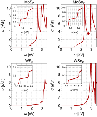
Once we have the tight-binding models for the four compounds, we can use them to calculate physical observables as, for example, the optical conductivity . For this aim we use the Kubo formula
where is the area of the unit cell, is the eigenstate of energy , is the Fermi-Dirac distribution function, in terms of the inverse temperature and considering that the Fermi energy lies in the gap, and is the velocity operator. The results are shown, for the approximate range of validity of our TB models ( eV above and below the band gap), in Fig. 5. We observe that, for all the compounds there is a threshold for the onset of optical transitions that is equal to the gap . The steplike structure of at low energies (see insets of each panel in Fig. 5) is due to the SOC, that leads to two set of optical transitions in the spectrum. Due to the stronger SOC of heavier W atoms, the effect is specially visible in WS2 and WSe2, with plateaus of eV in , corresponding to the energy splitting of the valence band at the K and K’ points of the Brillouin zone (see Fig. 3). These transitions lead to the well known A and B absorption peaks observed in photoluminescence.Mak et al. (2012) We further notice that our results for the optical conductivity are in good agreement, even for the onset energy, with experimental measurements (see e.g. Ref. Mak et al., 2010). At higher energies, the optical conductivity shows a series of peaks that are associated to optical transitions between flat bands in the spectrum (van Hove singularities). Such van Hove singularities are clearly evident for the valence and conduction bands at the M point of the Brillouin zone (see Fig. 3). We notice that disorder (vacancies, adatoms, etc.), not included here, can lead to the creation of midgap states that allows for additional optical transitions in the spectrum.Yuan et al. (2014)
VI Summary
In summary, we have generalized the tight-binding model for MoS2 of Ref. Cappelluti et al., 2013 to the other families of semiconducting TMDs: MoSe2, WS2 and WSe2. Our main result is the set of Slater-Koster parameters of Table 2, which have been obtained from a fit to DFT calculations in which special care was paid to capture the main orbital contribution of the TB bands at the relevant regions of the band structure. The obtained models have been used to calculate the optical conductivity of the different compounds. This approximation can be straightforwardly generalized to multi-layer systems with arbitrary stacking orders, heterostructures made from the stacking of layers of different compounds, twisted multilayers, strained and/or disordered samples, etc.
Acknowledgements.
We appreciate useful conversations with E. Cappelluti, P. Ordejón, F. Guinea, M.P. López-Sancho and H. Rostami. J.A. S.-G. acknowledges financial support from European Union’s Seventh Framework Programme (FP7/2007- 2013) through the ERC Advanced Grant NOV- GRAPHENE (GA 290846). P. S-J. was supported by MINECO through Grant No. FIS2015-65706-P and the Ramón y Cajal programme RYC-2013-14645. R.R. acknowledges financial support from MINECO (FIS2014-58445-JIN).References
- Novoselov et al. (2005) K. S. Novoselov, D. Jiang, F. Schedin, T. J. Booth, V. V. Khotkevich, S. V. Morozov, and A. K. Geim, “Two-dimensional atomic crystals,” Proc. Natl. Acad. Sci. USA 102, 10451–10453 (2005).
- Wang et al. (2012) Qing Hua Wang, Kourosh Kalantar-Zadeh, Andras Kis, Jonathan N. Coleman, and Michael S. Strano, “Electronics and optoelectronics of two-dimensional transition metal dichalcogenides,” Nature Nanotech. 7, 699 (2012).
- Jariwala et al. (2014) Deep Jariwala, Vinod K. Sangwan, Lincoln J. Lauhon, Tobin J. Marks, and Mark C. Hersam, “Emerging device applications for semiconducting two-dimensional transition metal dichalcogenides,” ACS Nano 8, 1102–1120 (2014).
- Ganatra and Zhang (2014) Rudren Ganatra and Qing Zhang, “Few-layer mos2: A promising layered semiconductor,” ACS Nano 8, 4074–4099 (2014).
- Feng et al. (2012) Ji Feng, Xiaofeng Qian, Cheng-Wei Huang, and Ju Li, “Strain-engineered artificial atom as a broad-spectrum solar energy funnel,” Nature Photonics 6, 866–872 (2012).
- Pan and Zhang (2012) Hui Pan and Yong-Wei Zhang, “Tuning the electronic and magnetic properties of mos2 nanoribbons by strain engineering,” The Journal of Physical Chemistry C 116, 11752–11757 (2012).
- Peelaers and Van de Walle (2012) Hartwin Peelaers and Chris G Van de Walle, “Effects of strain on band structure and effective masses in mos 2,” Phys. Rev. B 86, 241401 (2012).
- Scalise et al. (2014) E. Scalise, M. Houssa, G. Pourtois, V.V. Afanas?ev, and A. Stesmans, “First-principles study of strained 2d mos2,” Physica E: Low-dimensional Systems and Nanostructures 56, 416 – 421 (2014).
- Molina-Sánchez et al. (2015) Alejandro Molina-Sánchez, Kerstin Hummer, and Ludger Wirtz, “Vibrational and optical properties of mos2: From monolayer to bulk,” Surface Science Reports 70, 554 – 586 (2015).
- Brumme et al. (2015) Thomas Brumme, Matteo Calandra, and Francesco Mauri, “First-principles theory of field-effect doping in transition-metal dichalcogenides: Structural properties, electronic structure, hall coefficient, and electrical conductivity,” Phys. Rev. B 91, 155436 (2015).
- Zhu et al. (2011) Z. Y. Zhu, Y. C. Cheng, and U. Schwingenschlögl, “Giant spin-orbit-induced spin splitting in two-dimensional transition-metal dichalcogenide semiconductors,” Phys. Rev. B 84, 153402 (2011).
- Xiao et al. (2012) Di Xiao, Gui-Bin Liu, Wanxiang Feng, Xiaodong Xu, and Wang Yao, “Coupled spin and valley physics in monolayers of and other group-vi dichalcogenides,” Phys. Rev. Lett. 108, 196802 (2012).
- Xu et al. (2014) Xiaodong Xu, Wang Yao, Di Xiao, and Tony F Heinz, “Spin and pseudospins in layered transition metal dichalcogenides,” Nature Physics 10, 343–350 (2014).
- Babaee Touski et al. (2016) S. Babaee Touski, M. Pourfath, R. Roldán, and M. P. López-Sancho, “Enhanced Spin-Flip Scattering by Surface Roughness in WS and MoS Nanoribbons,” ArXiv e-prints (2016), arXiv:1606.03339 .
- Zeng et al. (2012) H. Zeng, J. Dai, W. Yao, D. Xiao, and X. Cui, “Valley polarization in mos2 monolayers by optical pumping,” Nature Nanotech. 7, 490 (2012).
- Mak et al. (2012) Kin Fai Mak, Keliang He, Jie Sahn, and Tony F. Heinz, “Control of valley polarization in monolayer mos2 by optical helicity,” Nature Nanotech. 7, 494 (2012).
- Cao et al. (2012) T. Cao, G. Wang, W. Han, H. Ye, C. Zhu, J. Shi, Q. Niu, P. Tan, E. Wang, B. Liu, and J. Feng, “Valley-selective circular dichroism of monolayer molybdenum disulphide.” Nature Commun. 3, 887 (2012).
- Zeng et al. (2013) Hualing Zeng, Gui-Bin Liu, Junfeng Dai, Yajun Yan, Bairen Zhu, Ruicong He, Lu Xie, Shijie Xu, Xianhui Chen, Wang Yao, and Xiaodong Cui, “Optical signature of symmetry variations and spin-valley coupling in atomically thin tungsten dichalcogenides,” Scientific Reports 3, 1608 (2013).
- Wu et al. (2013) Sanfeng Wu, Jason S Ross, Gui-Bin Liu, Grant Aivazian, Aaron Jones, Zaiyao Fei, Wenguang Zhu, Di Xiao, Wang Yao, David Cobden, and X. Xu, “Electrical tuning of valley magnetic moment through symmetry control in bilayer mos2,” Nature Physics 9, 149 (2013).
- Wang et al. (2013) Qinsheng Wang, Shaofeng Ge, Xiao Li, Jun Qiu, Yanxin Ji, Ji Feng, and Dong Sun, “Valley carrier dynamics in monolayer molybdenum disulfide from helicity-resolved ultrafast pump–probe spectroscopy,” ACS Nano 7, 11087–11093 (2013).
- Mak et al. (2013) Kin Fai Mak, Keliang He, Changgu Lee, Gwan Hyoung Lee, James Hone, Tony F. Heinz, and Jie Shan, “Tightly bound trions in monolayer mos2,” Nature Mat. 12, 207 (2013).
- Sallen et al. (2012) G. Sallen, L. Bouet, X. Marie, G. Wang, C. R. Zhu, W. P. Han, Y. Lu, P. H. Tan, T. Amand, B. L. Liu, and B. Urbaszek, “Robust optical emission polarization in mos2 monolayers through selective valley excitation,” Phys. Rev. B 86, 081301 (2012).
- Kormányos et al. (2014) Andor Kormányos, Viktor Zólyomi, Neil D. Drummond, and Guido Burkard, “Spin-orbit coupling, quantum dots, and qubits in monolayer transition metal dichalcogenides,” Phys. Rev. X 4, 011034 (2014).
- Kormányos et al. (2015) Andor Kormányos, Guido Burkard, Martin Gmitra, Jaroslav Fabian, Viktor Zólyomi, Neil D Drummond, and Vladimir Fal’ko, “k * p theory for two-dimensional transition metal dichalcogenide semiconductors,” 2D Materials 2, 022001 (2015).
- Roldán et al. (2015) R. Roldán, A. Castellanos-Gomez, E. Cappelluti, and F. Guinea, “Strain engineering in semiconducting two-dimensional crystals,” J. of Phys.: Condens. Matter 27, 313201 (2015).
- San-Jose et al. (2016) Pablo San-Jose, Vincenzo Parente, Francisco Guinea, Rafael Roldán, and Elsa Prada, “Inverse funnel effect of excitons in strained black phosphorus,” Phys. Rev. X 6, 031046 (2016).
- Wu et al. (2014) Wenzhuo Wu, Lei Wang, Yilei Li, Fan Zhang, Long Lin, Simiao Niu, Daniel Chenet, Xian Zhang, Yufeng Hao, Tony F Heinz, and Zhong L. Hone, James Wang, “Piezoelectricity of single-atomic-layer mos2 for energy conversion and piezotronics,” Nature 514, 470–474 (2014).
- Roldán et al. (2014) Rafael Roldán, Jose A. Silva-Guillén, M. Pilar López-Sancho, Francisco Guinea, Emmanuele Cappelluti, and Pablo Ordejón, “Electronic properties of single-layer and multilayer transition metal dichalcogenides mx2 (m = mo, w and x = s, se),” Annalen der Physik 526, 347–357 (2014).
- Yuan et al. (2014) Shengjun Yuan, Rafael Roldán, M. I. Katsnelson, and Francisco Guinea, “Effect of point defects on the optical and transport properties of and ,” Phys. Rev. B 90, 041402 (2014).
- Rostami et al. (2015) Habib Rostami, Rafael Roldán, Emmanuele Cappelluti, Reza Asgari, and Francisco Guinea, “Theory of strain in single-layer transition metal dichalcogenides,” Phys. Rev. B 92, 195402 (2015).
- Pearce and Burkard (2015) A. J. Pearce and G. Burkard, “A Tight Binding Approach to Strain and Curvature in Monolayer Transition-Metal Dichalcogenides,” ArXiv e-prints (2015), arXiv:1511.06254 [cond-mat.mes-hall] .
- Rostami et al. (2015) H. Rostami, R. Asgari, and F. Guinea, “Edge modes in zigzag and armchair ribbons of monolayer MoS,” ArXiv e-prints (2015), arXiv:1511.07003 .
- Farmanbar et al. (2016) Mojtaba Farmanbar, Taher Amlaki, and Geert Brocks, “Green’s function approach to edge states in transition metal dichalcogenides,” Phys. Rev. B 93, 205444 (2016).
- Castellanos-Gomez et al. (2013) Andres Castellanos-Gomez, Rafael Roldán, Emmanuele Cappelluti, Michele Buscema, Francisco Guinea, Herre S. J. van der Zant, and Gary A. Steele, “Local strain engineering in atomically thin mos2,” Nano Letters 13, 5361 (2013).
- Cappelluti et al. (2013) E. Cappelluti, R. Roldán, J. A. Silva-Guillén, P. Ordejón, and F. Guinea, “Tight-binding model and direct-gap/indirect-gap transition in single-layer and multilayer mos2,” Phys. Rev. B 88, 075409 (2013).
- Liu et al. (2013) Gui-Bin Liu, Wen-Yu Shan, Yugui Yao, Wang Yao, and Di Xiao, “Three-band tight-binding model for monolayers of group-vib transition metal dichalcogenides,” Phys. Rev. B 88, 085433 (2013).
- Kośmider et al. (2013) K. Kośmider, J. W. González, and J. Fernández-Rossier, “Large spin splitting in the conduction band of transition metal dichalcogenide monolayers,” Phys. Rev. B 88, 245436 (2013).
- Kumar and Ahluwalia (2012) A Kumar and PK Ahluwalia, “Electronic structure of transition metal dichalcogenides monolayers 1h-mx2 (m= mo, w; x= s, se, te) from ab-initio theory: new direct band gap semiconductors,” The European Physical Journal B 85, 1–7 (2012).
- Note (1) DFT calculations were done using the Siesta code,SS02; AS08 with the exchange-correlation potential of Ceperly-AlderCA80 as parametrized by Perdew and Zunger.PZ81 A split-valence double- basis set including polarization functions was considered.AS99 The energy cutoff and the BZ sampling were chosen to converge the total energy with a value of 300 Ry and . The energy cutoff was set to eV. Spin-orbit interaction of the different compounds was considered by following the method developed in Ref. \rev@citealpnumFF06. The lattice parameters used in the calculation are given in Table 1.
- Roldán et al. (2014) R Roldán, M P López-Sancho, F Guinea, E Cappelluti, J A Silva-Guillén, and P Ordejón, “Momentum dependence of spin–orbit interaction effects in single-layer and multi-layer transition metal dichalcogenides,” 2D Mater. 1, 034003 (2014).
- Slater and Koster (1954) J. C. Slater and G. F. Koster, “Simplified lcao method for the periodic potential problem,” Phys. Rev. 94, 1498–1524 (1954).
- Ridolfi et al. (2015) E Ridolfi, D Le, T S Rahman, E R Mucciolo, and C H Lewenkopf, “A tight-binding model for mos 2 monolayers,” Journal of Physics: Condensed Matter 27, 365501 (2015).
- Fang et al. (2015) Shiang Fang, Rodrick Kuate Defo, Sharmila N. Shirodkar, Simon Lieu, Georgios A. Tritsaris, and Efthimios Kaxiras, “Ab initio tight-binding hamiltonian for transition metal dichalcogenides,” Phys. Rev. B 92, 205108 (2015).
- Note (2) The calculation of tight-binding band structure and fitting to DFT have been performed using the MathQ package, developed by P. San-Jose. (Source: http://www.icmm.csic.es/sanjose/MathQ/MathQ.html).
- Lado and Fernandez-Rossier (2016) J. L. Lado and J. Fernandez-Rossier, “Landau Levels in two dimensional materials from first principles,” ArXiv e-prints (2016), arXiv:1606.03038 .
- Mak et al. (2010) Kin Fai Mak, Changgu Lee, James Hone, Jie Shan, and Tony F. Heinz, “Atomically thin : A new direct-gap semiconductor,” Phys. Rev. Lett. 105, 136805 (2010).
Appendix A On-site and hopping matrices of the block
For convenience we reproduce in this appendix the analytical expressions for the model. The on-site terms of the Hamiltonian can be written in the compact form:Roldán et al. (2014)
| (8) |
where
| (9) |
where and are the SOC of the metal () and chalcogen atoms (), respectively, and is the -component of the spin degree of freedom.Roldán et al. (2014) The effects of vertical hopping between top and bottom atoms is considered through the terms , and . The nearest neighbor hopping between and atoms are
| (10) | ||||
| (11) | ||||
| (12) |
Appendix B Orbital contribution of the tight-binding bands
In this appendix we show the orbital contribution of the tight-binding bands, as compared to the DFT results, for MoSe2 (Fig. 6), WS2 (Fig. 7) and WSe2 (Fig. 8).