Pressure effects on crystal and electronic structure of bismuth tellurohalides
Abstract
We study the possibility of pressure-induced transitions from a normal semiconductor to a topological insulator (TI) in bismuth tellurohalides using density functional theory and tight-binding method. In BiTeI this transition is realized through the formation of an intermediate phase, a Weyl semimetal, that leads to modification of surface state dispersions. In the topologically trivial phase, the surface states exhibit a Bychkov-Rashba type dispersion. The Weyl semimetal phase exists in a narrow pressure interval of 0.2 GPa. After the Weyl semimetal–TI transition occurs, the surface electronic structure is characterized by gapless states with linear dispersion. The peculiarities of the surface states modification under pressure depend on the band-bending effect. We have also calculated the frequencies of Raman active modes for BiTeI in the proposed high-pressure crystal phases in order to compare them with available experimental data. Unlike BiTeI, in BiTeBr and BiTeCl the topological phase transition does not occur. In BiTeBr, the crystal structure changes with pressure but the phase remains a trivial one. However, the transition appears to be possible if the low-pressure crystal structure is retained. In BiTeCl under pressure, the topological phase does not appear up to 18 GPa due to a relatively large band gap width in this compound.
pacs:
73.43.Nq, 73.20.At, 78.40.Kc, 78.30.Am, 62.50.-pI INTRODUCTION
Materials with strong spin-orbit coupling (SOC) open up exciting possibilities in the rapidly developing area of solid state physics – spintronics. Such perspective materials are, for example, topological insulators (TI) which simultaneously combine the properties of a semiconductor in the bulk and a metal on the surface.pankratov_1987 ; fu_2007 ; xia_2009 ; eremeev_2010 ; eremeev_landolt_2012 The metallic behavior of the surface is caused by the presence of special spin-polarized surface states with Dirac-type dispersions which are topologically protected from backscattering. Other promising candidates for spintronics are bismuth tellurohalides (BiTe, =I,Br,Cl). These non-centrosymmetric compounds are topologically trivial but characterized by a giant Bychkov-Rashba-type spin splitting BR of bulk and surface electronic bands.ishizaka_2011 ; bahramy_2011 ; eremeev_2012 ; eremeev_jetpl_2012 ; landolt_2012 ; crepaldi_2012 ; rusinov_2013 ; sakano_2013 ; eremeev_bitebr . Both topological insulators and bismuth tellurohalides can be used for designing new spintronic and magnetoelectric devices such as spin transistors dolcini ; krueckl ; datta-das ; datta-das2 as well as for the creation of quantum computers.
Recently it was predicted that BiTeI transforms from a trivial phase into a topological insulator by applying an external pressure of 1.7–4.1 GPa.bahramy2_2012 ; bahramy_2012 The topological phase transition (TPT) was also observed experimentally at 2–2.9 GPa and 3.5 GPa using infrared spectroscopy xi2013 and Shubnikov-de Haas oscillations measurements,ideue2014 respectively. In Ref. 27, within optical measurements the TPT doesn’t observed. In the theoretical study within density functional theory (DFT) the TPT was found at 4.5 GPa.chen_JPCC Using ab initio based tight-binding (TB) calculations it was shown vanderbilt2014 that the TPT is accompanied by the formation of an intermediate phase, a Weyl semimetal, which is characterized by one or more pairs of band-touching points (Weyl nodes) between valence and conduction bands. The possibility of topological phase transition in the related tellurohalides, BiTeBr and BiTeCl, has not been studied yet.
To draw a conclusion about the existence of pressure-induced topological phases in these compounds, one should first find out whether any pressure-induced crystal phase transitions (CPT) would occur under pressure. In the case of BiTeI, the experimental observation of x-ray diffraction xi2013 ; chen_JPCC and Raman ponosov2013 ; tran2014 spectra reveals the CPT at pressure of 8–9 GPa which is by factor of 2-3 higher then the pressure of TPT. In Ref. chen_JPCC, , the orthorhombic Pnma structure was proposed as a high-pressure phase by comparing the DFT-obtained enthalpy for the low-pressure phase and Pnma. It was also shown that this hexagonal–orthorhombic CPT occurs at a pressure of 6 GPa.chen_JPCC For the BiTeBr compound, the CPT has been experimentally observed at similar pressures (6–7 GPa).manjon_2016
A thorough investigation of the topological transition in BiTeI requires a careful consideration of surface electronic properties. The fact is that in the bismuth tellurohalides, the band-bending is of special significance because this effect induces additional spin-polarized surface states which have been observed both in angle resolved photoemission spectroscopy (ARPES) measurements and in DFT calculations eremeev_2012 ; landolt_2012 ; crepaldi_2012 ; sakano_2013 . The band-bending arises from the polar nature of the compounds and is caused by a charge redistribution at the surface–vacuum boundary. The redistribution changes the effective potential level in the surface region relatively to the bulk and, thereby, shifts the chemical potential near the surface. Till now the surface electronic structure of BiTeI under pressure has been investigated without taking into account the band-bending.
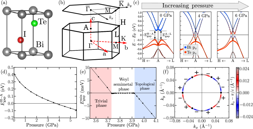
Here we present a theoretical study both of the topological and crystal phase transitions in the bismuth tellurohalides. In the case of BiTeI, we demonstrate the features of bulk and surface electronic spectra in the topologically trivial phase, in the case of Weyl semimetal and in the topological insulator. It is found that the intermediate phase in BiTeI, a Weyl semimetal, appears in the pressure range of 3.7–3.9 GPa which can be experimentally detected. It is also shown that the effect of band-bending plays a crucial role in the surface electronic structure formation. By tracing the modification of surface electronic spectra with pressure the mechanism of changing the dispersion of surface states is revealed. An analysis of BiTeBr and BiTeCl shows the absence of TPT in these compounds. In BiTeBr, a crystal phase transition occurs before the TPT that precludes the latter. In BiTeCl, the topological phase does not appear due to a relatively large band gap at zero pressure.
II RESULTS AND DISCUSSION
II.1 COMPUTATIONAL DETAILS
The bulk electronic structure calculations were carried out within DFT using the projector augmented-wave (PAW) method realized in the VASP code and the PBE exchange-correlation functional pbe . The spin-orbit coupling was accounted by a second-variation method. Crystal lattice parameters and atomic positions were optimized for pressures up to 8, 10, 18 GPa for BiTeI, BiTeBr and BiTeCl, respectively, using PBE exchange-correlation functional. Under the structural relaxation the crystal symmetry kept the same. The optimization was performed for all structures of BiTeX (X=I, Cl, Br) considered in the paper. At zero pressure, for BiTeI and BiTeCl compounds overstimation of and parameters is 2% and 7%, respectively. For BiTeBr compound —2% and 6%, respectively.
For simulation surface under pressure, the large slab has been constructed on the basis relaxed parameters of bulk structure under the pressure. The large slab Hamiltonian derived from the bulk one is then used to calculate surface Green functions. Sancho:84 ; Sancho:85 ; Henk:93 So, tight-binding models were constructed using WANNIER90 code.marzari ; WZhang . The chosen basis consists of six spinor -type orbitals for each atom: , , , , , . The low-lying orbitals are not taken into consideration. To study the bulk electronic spectra near the point of TPT two tight-binding Hamiltonians are constructed: one for the topologically trivial phase of BiTeI and the other for the TI phase, and , respectively. For each intermediate pressure the Hamiltonian is taken as a linear combination: . Here and correspond to a pressure of 3.6 GPa and 4 GPa, respectively.
The band-bending effect was accounted by shifting the on-site matrix elements of surface atoms. The value of shifting is determined by the potential gradient obtained in the first-principles calculations for slabs of BiTeX (X=I, Cl, Br) at zero pressure.eremeev_2012 ; eremeev_bitebr These values of band bending shift were applied for all surfaces of BiTeX (X=I, Cl, Br) under pressure.
Dynamical properties of the bulk bismuth tellurohalides were calculated within the density-functional perturbation theoryzein in a mixed-basis pseudopotential approach.Louie:79 ; Meyer ; Heid:99 . The details of the calculation as well as the spin-orbit coupling implementation within the mixed-basis pseudopotential method can be found in Ref. Heid:10, ; Sklyadneva, .
II.2 Bulk band structure of BiTeI
BiTeI crystalizes in a hexagonal structure, P3m1 (Fig. 1(a)). At zero pressure, the compound is a semiconductor. Using fully optimized crystal structure parameters (, and atomic coordinates), we obtained the band gap width of 408 meV which is in good agreement both with experimental measurements (380 meV ishizaka_2011 ) and -calculations (400 meV in the LDA+ scheme rusinov_2013 ). Such an agreement which is unusual for DFT is explained by some overestimation of structural parameters in the relaxation process.
The valence and conduction gap edge bands are composed of tellurium and bismuth states (Fig. 1(c)), respectively. A strong spin-orbit interaction leads to a large Bychkov-Rashba type spin splitting of the bulk states and thus two pairs of extrema along the H-A-L line are formed: () and (). Under pressure the value of diminishes and at a certain pressure,, shrinks to zero that indicates normal semiconductor-Weyl semimetal transition. These doesn’t happen with gap along the A-L direction, . Upon further increase of pressure a band gap appears with inverted edges in the vicinity of the A point: now the lowest conduction band is formed by tellurium states while the top valence band consists of bismuth orbitals (Fig. 1(c)). The calculated value of equal to 3.73 GPa (Fig. 1(d)) agrees well with the experimental one, = 3.5 GPa.xi2013 ; ideue2014
Due to a small overestimation of the band gap compared to the experimental value (7%), the parameter is also slightly overestimated. The calculated value of =3.5 GPa contradicts =10 GPa obtained in the calculation.tran2014 As a result according to the Ref.27 the =10 GPa indicates the impossibility of TPT in BiTeI due to the crystal phase transition at 9 GPa. The discrepancy is explained by a strong overestimation of the band gap width at zero pressure in the calculations. Switching on the corrections on Van der Waals forces lead to a strong underestimation of the band gap at zero pressure ( 230 meV). For this reason, we do not present the results obtained after the relaxation of crystal structure with van der Waals corrections.
The behaviour of band gap and the trajectory of crossing (Weyl) points near the topological phase transition are plotted in Figs. 1(e) and (f). is the smallest value of in the entire BZ. The position of Weyl points in the reciprocal space depends on the value of pressure. The Weyl points are formed at the BZ boundary, , along each AH direction. At the phase transition pressure, , each Weyl point splits up into pair of nodes with a clockwise and counterclockwise propagation on the () plane (Fig. 1(f)). Also, these two nodes shift in opposite directions along . The Weyl points are observed up to 3.93 GPa and then the band degeneracy is lifted and BiTeI converts into a topological insulator. Thus, the Weyl semimetal phase exists within the pressure interval from 3.73 to 3.93 GPa. The range is not small, so the phase can be experimentally observed.
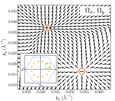
The pairs of Weyl points appeared along the AH directions have opposite topological charges (chirality) which are defined by Chern numbers as the flux of Berry phase gauge field over a sphere around each Weyl point: , where – surface normal vector and is the Berry curvature. Here is the Berry connection defined as for n-th Bloch state, , (in our case – the highest occupied band) with quantum number . The calculation reveals that the Weyl points which move clockwise (counterclockwise) have a positive (negative) Chern number, =1 (-1), that corresponds to drain (source) points of the Berry gauge field. The in-plane components of the Berry curvature at Å-1 are demonstrated in Fig. 2.
II.3 Surface band structure of BiTeI
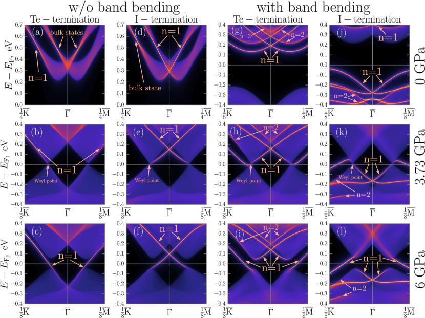
To illustrate surface electronic properties of the systems with Bychkov-Rashba-type spin splitting of bands in the topological and Weyl semimetal phases we considered within tight-binding method a hypothetical model of the bismuth tellurohalides surface under pressure. As was mentioned above to construct the surface under pressure we used large slab with fully relaxed parameters of the bulk structure under the pressure. To do the model more realistic, we included the effect of band bending because of lack of inversion symmetry in the bismuth tellurohalides.
The topological phase transition is accompanied by qualitative changes in the surface electronic structure. The BiTeI has two possible surface terminations: iodine or tellurium with positive and negative band bending, respectively. eremeev_2012 ; eremeev_jetpl_2012 Let us first trace the evolution of surface electronic states with pressure without considering the effect of band bending (see Fig. 3(a–f)). In the absence of external pressure (Figs. 3(a) and (d)), the surface states on the Te(I)-terminated surface appear along the outer (inner) brunch of unoccupied spin-orbit split bulk bands and are mainly localized in the topmost trilayer.
In the pressure-induced Weyl semimetal phase (Figs. 3(b) and (e)), the surface states on the Te-terminated surface remain along the outer edge of the bulk bands while in the case of iodine termination they shift into the band gap and exhibit a cone-like dispersion with crossing at the BZ center. The surface states touch the crossing (Weyl) points of the conduction and valence bulk bands. In the topological phase (Figs. 3(c) and (f)), the surface states become gapless linking the valence and conduction bands. In the case of I-terminated surface, the crossing of two surface states occurs in the band gap slightly above the bulk conduction band minima while on the Te-terminated surface the crossing (Dirac) point is inside off the valence bands due to the mixing of surface and bulk electronic bands.
The surface electronic structure obtained with taking into account the effect of band bending as well as its evolution under pressure is different. The overall band structure is strongly modified because a set of well-defined Bychkov-Rashba type spin split surface bands appearing due to the band-bending effect.bahramy2_2012 In the topologically trivial phase (Figs. 3(g) and (j)), the lowest surface band on the Te-terminated surface lies within the energy gap and is strongly localized in the topmost trilayer. The states with higher energies are confined within three upper trilayers. On the I-terminated surface, a set of surface bands splits off from the valence bulk band. The occupied surface electronic states appear mainly inside or at the edge of the bulk bands except the topmost state which is shifted upwards into the energy gap. Such a hierarchy of surface states was also observed in ARPES experiments.landolt_2012 ; sakano_2013 In the Weyl semimetal phase (Figs. 3(h) and (k)), when passing through the bulk Weyl nodes the surface states localized in the upper trilayer become discontinuous. In the topological phase (Fig. 3(i) and (l)), the surface states are breaking up into two parts near the bulk edge extrema, and gapless surface states with a linear dispersion in the band gap are formed. On both surface terminations, the crossing point of the gapless surface states is inside the bulk bands where they turn into surface resonances.
II.4 Fermi arcs in Weyl-semimetal phase of BiTeI
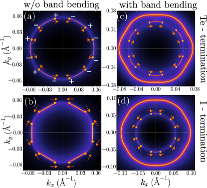
The surface electronic structure of Weyl semimetals is characterized by the presence of Fermi arcs connecting the Weyl points with opposite chirality. Figure 4 shows the electronic spectra at the Fermi level of the (001) surface for both terminations. The isoenergetic surface spectra were calculated with and without the account of the band-bending at a pressure of 3.84 GPa which corresponds to a Weyl semimetal phase (see Fig. 1(e)). Also shown are the positions of Weyl points on the () plane. The pairs of Weyl points lie on the trajectory connecting the positions of Weyl points at the pressure (3.73 GPa) and at the annihilation point (3.93 GPa) (see Fig. 1(f)).
Without taking band bending into account the Fermi arcs link up the pair of Weyl points induced originally along the A-H (–) direction of the bulk (surface) BZ. The form of Fermi arcs depends on the surface termination. On the Te-terminated surface, they form arc-like curves coinciding with the trajectory of a pair of nodes which move clockwise and counterclockwise over the BZ. In the case of I-termination, the Fermi arcs connect the pairs of Weyl points by a straight line. On further increase in pressure, the length of Fermi arcs increases and when the Weyl semimetal–TI phase transition occurs the arcs connect with each other forming a gapless topological surface state.
With the account of band bending, in addition to the Fermi arcs a circular surface state appears which originates from the outer branches of Bychkov-Rashba type spin split surface states (Figs. 3(h) and (k)). In the case of I-termination, the outer circular state is found farther from the surface BZ center as compared to the Te-terminated surface. However the isoenergetic curves for both terminations are qualitatively similar, unlike the previous case. In addition, with the account of band bending the Fermi arcs link up the Weyl points from neighbouring pairs. Upon increasing pressure, the length of Fermi arcs decreases up to zero at 3.9 GPa when the transition to topological phase occurs. After the transition the isoenergetic electronic structure is presented by a single closed curve of the topological surface state.
The formation of Fermi arcs is closely related to the spin texture of the surface states. Without account of band bending, the single closed contour in the topological phase has a clockwise spin helicity.bahramy_2012 In the Weyl semimetal phase, Fermi arcs inherit this behaviour — the helicity also has a clockwise character. The spin texture ”connects” the source and drain Weyl points in the clockwise order, so the Fermi arcs link up the pair of points emerged along the A-H direction.
Subject to the band bending, the situation is opposite. The Fermi arcs get the spin texture from the inner closed contour of Bychkov-Rashba type spin split surface states in the trivial phase which have a counterclockwise helicity.eremeev_jetpl_2012 The spin texture ”connects” the source and drain Weyl points in counterclockwise order, so the Weyl points from neighbouring pairs are connected.
Thus, in the calculations the modification of the surface state under pressure depends on whether the band-bending effect is taken into account or not. The modifications are closely related to the alteration of the Fermi arcs which characterize the isoenergetic spectra of Weyl semimetals. Our additional calculations revealed that this picture does not change qualitatively with a strong modification of band bending potential. Also, all prognosticated peculiarities of the BiTeI surface electronic structure in topological phase can be revealed in other noncentrosymmetric alloys where the appearance of the topological or trivial phases can depends, for instance, on the concentrations. Note, such systems were proposed in Ref. 25 and shown that in cases LaBi1-xSbxTe3, LuBi1-xSbxTe3 the topological phase can be induced by variation of the Sb concentration, .
II.5 Crystal phase transition in BiTeI
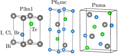
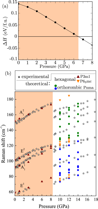
Since BiTeI undergoes crystal phase transitions (CPT) under hydrostatic compression xi2013 ; chen_JPCC ; ponosov2013 ; tran2014 it is necessary to compare the pressures corresponding to the TPT and CPT. The X-Ray diffraction dataxi2013 ; chen_JPCC showed that BiTeI remained in the P3m1 (ambient pressure) structure up to 8–9 GPa. The stability of the hexagonal phase up to 9 GPa was also confirmed by high-pressure Raman spectra measurements.ponosov2013 ; tran2014 For the higher pressure phase the orthorhombic Pnma structure with 12 atoms per unit cell were suggested (see Fig. 5).chen_JPCC As our calculation show, this structure is normal non-direct gap semiconductor. We calculated the difference in enthalpy between the hexagonal P3m1 and orthorhombic Pnma phases depending on pressure (Fig. 6(a)). As follows from the calculation the CPT should occur at 6.5 GPa. This value is somewhat smaller than the experimental CPT pressure. Despite this discrepancy, the CPT takes place after the topological phase transition and at pressures which are beyond the pressure range (3.73–3.93 GPa) where the Weyl semimetal phase exists. Thus the CPT is accompanied by a TPT from a topological insulator to a normal semiconducting phase.
To additionally verify the proposed structure we have also calculated Raman mode frequencies for the P3m1 phase up to 8 GPa and for the Pnma structure at pressures 10, 12, and 14 GPa (Fig. 6(b)). In the hexagonal P3m1 phase with 3 atoms per unit cell, there are two A1 and two E (twofold degenerate) zone center optical modes, which are both Raman and infrared active because of the lack of inversion symmetry. At pressures below the CPT, the theoretical data are in excellent agreement with experimental results with the exception of mode E1 between 4–8 GPa where experimental data are absent apparently due to decreasing of the mode intensity. In the experimental Raman spectraponosov2013 ; tran2014 three modes are visible up to 8 GPa with an expected increase upwards with pressure. A sudden change in the number and frequency of Raman active modes which points out to a structural transition is observed at 9 GPa.
The Raman spectrum for the orthorhombic phase has a rather complicated character. All the modes are non degenerate. Some of them coincide with the experimental data. In general, variation of Raman mode frequencies with pressure (10–12–14 GPa) resembles the behaviour of the experimental Raman modes. However, the number of the calculated Raman modes in the Pnma structure (13 are shown in the figure while the total number of Raman modes is equal to 18) is almost twice as large as the experimental data. Although the experimental Raman spectrum at high pressures bears some similarity to the calculated Pnma spectrum the measured modes apparently correspond to a more symmetric structure. The character of the measured spectrum indicates some orthorhombic phase with similar enthalpy.
Another candidatetran2014 can be the hexagonal P6c structure with 6 atoms per unit cell which is the structure of another compound, BiTeCl, at ambient pressure.shevelkov The Raman active modes calculated for BiTeI in the hexagonal P6c structure at 10 and 12 GPa are continuations of the corresponding modes in the low-pressure phase. The number of E modes is doubled and the two lower E modes are shifted down in energy compared to the E1. So the Raman spectrum does not reproduce the high-pressure experimental data and the P6c structure cannot be considered as a high-pressure phase of BiTeI.
II.6 Electronic properties of BiTeBr and BiTeCl
For BiTeBr and BiTeCl there is no experimental information about the possibility of topological phase transition under pressure. It was thought that BiTeBr crystallizes in the hexagonal structure, Pm1, with Te and Br atoms statistically distributed within two layers adjacent to the Bi layer.shevelkov Later an ordered stacking of Te and Br sublattices, like in BiTeI, was confirmed by x-ray diffraction measurements and, moreover, ARPES images revealed a well-defined Bychkov-Rashba type spin split states.sakano_2013 The structure of BiTeCl at ambient pressure is hexagonal, P6c, with 6 atoms per unit cell.shevelkov We also considered BiTeCl in the P3m1 crystal phase which was found in the calculation to be energy preferable up to the CPT. To evaluate the probability of CPT we also examine both compounds in the orthorhombic Pnma structure which was originally proposed as a high-pressure structure for BiTeI.chen_JPCC This phase is considered for BiTeBr and BiTeCl compounds because most V-VI-VII semiconductors crystallize in this structure.donges_1950 ; donges_1950_2 ; donges_1951 ; kikuchi_1967
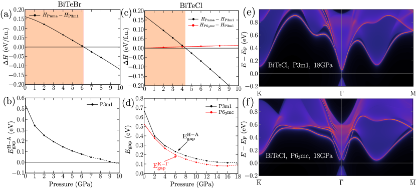
As follows from Fig. 7(a) the CPT in BiTeBr takes place at a pressure of 6.3 GPa. Although the band gap (Fig. 7(b)) decreases with pressure its lowest value is of 80 meV at the point of CPT and therefore the system possesses a trivial topology. The CPT pressure is in good agreement with experimental results of Ref. manjon_2016 . The data exclude the possibility of TPT in the low-pressure phase of BiTeBr. Note, if another high-pressure structure which is energy preferable compared to the P3m1 and Pnma structures is realized then the pressure of CPT would be lower than 6.3 GPa and in any case the CPT occurs before a TPT.
Due to relatively closer the pressures of TPT and CPT and lacking of experimental investigations of both transitions, additional calculations have been provided by inclusion van der Waals correction within DFT-D3 DFT-D3 scheme. So, the correction lead to shifting CPT and TPT in the area of smallest pressures: 4 GPa and 8 GPa, respectively. However, the conclusion is preserved: in BiTeBr TPT is absent.
The case of BiTeCl is more complicated from the crystallographic point of view. First of all, our results indicate the possibility of CPT from P63mc to the P3m1 structure at very small pressures because the calculated difference in enthalpy (Fig. 7(c)), red line) turns out to be 0.8 meV even at zero pressure. With increasing pressure, the P3m1 phase remains energy preferable up to 4.3 GPa when the CPT to the Pnma structure takes place.
However, these results do not affect the general conclusion about a possibility of TPT in this compound. A TPT does not occur either in the P3m1 or in the P63mc crystal phases because although the band gap width decreases with pressure (Fig. 7(d)) this decreasing practically ceases at a value of 100 meV (80 meV) for the P3m1 (P63mc) structure. A relatively large band gap width makes impossible the TPT both in the P3m1 and in the P63mc hexagonal phase.
This conclusion contradicts the data reported in Ref. chen_Nature, where by APRES measurements a topological insulator phase in BiTeCl with Dirac-type surface states was found at zero pressure. The observation of the TI phase might be explained by a possible crystallization of the material in another hexagonal structure what is confirmed by a very small bulk band gap width (220 meV) obtained in the experiment. The latter contradicts the electronic structure calculations within the GW-approximation that reveal the band gap width of 800-900 meV.rusinov_2013 .
For additional verification of the trivial character of BiTeCl in the hexagonal phases, we have calculated the surface electronic structure at a pressure of 18 GPa with taking into account the band bending effect. Figures 7(e) and (f) show the electronic spectra of the Te-terminated surface for the P3m1 and P63mc crystal phases, respectively. It is obvious that there are no topological surface states in the bulk band gap and therefore the system is a trivial semiconductor. Both crystal phases are only characterized by the presence of well known Bychkov-Rashba type split surface states. It should be noted, that additional extrema of the conduction band appear, one at the point and the other in the - direction which results in an indirect band gap in the case of the P63mc structure.
III CONCLUSIONS
We have investigated a possibility of topological phase transitions in bismuth tellurohalides. For BiTeI, our results support the pressure-induced TPT in agreement with experimental data.xi2013 ; chen_JPCC ; ideue2014 . The study of bulk and surface electronic structures of BiTeI under pressure revealed that an intermediate phase, a Weyl semimetal, is formed during the transition from a trivial semimetal to a topological insulator in the pressure interval of 3.7–3.9 GPa. The range is not too small, so the intermediate phase can be experimentally observed. The inclusion of the band bending effect in the calculation allowed us to consider surface modifications caused by the polarity of BiTeI. As a result, we revealed the mechanism of changing of the surface states from a Bychkov-Rashba type spin split state to a gapless surface state that occurs during the TPT. In the TI phase, the surface states feature a linear dispersion which depends on the surface termination. This result is relevant for all asymmetric materials where TPT can be induced not only by applying hydrostatic pressure but also by a doping.
We have also compared the Raman mode frequencies obtained experimentally for BiTeI under pressure with those calculated for BiTeI. At low pressures the theoretical data for the P3m1 crystal phase reproduce well the experimental measurements. As for the high-pressure phases, the experimental Raman spectrum bears some similarity to the calculated spectrum in the Pnma phase but the measured modes apparently correspond to a more symmetric structure. We also showed the absence of TPT in BITeBr and BiTeCl. In BiTeBr, the CPT occurs before a TPT becomes possible. In BiTeCl, a relatively large value of band gap width prevents the possibility of TPT up to 18 GPa.
IV ACKNOWLEDGEMENTS
This study (research grant No. 8.1.05.2015) was supported by the Tomsk State University Academic D.I. Mendeleev Fund Program in 2015, by grant of Saint-Petersburg State University for scientific investigations No. 15.61.202.2015; the Spanish Ministry of Economy and Competitiveness MINECO Project FIS2013-48286-C2-1-P.
References
- (1) O.A. Pankratov, S.V. Pakhomov and B.A. Volkov, Solid State Communications 61, 93–96 (1987).
- (2) L. Fu, C.L. Kane and E.J. Mele, Phys. Rev. Lett. 98, 106803 (2007).
- (3) Y. Xia, D. Qian, D. Hsieh, L. Wray, A. Pal, H. Lin, A. Bansil, D. Grauer, Y.S. Hor, R.J. Cava, M.Z. Hasan, Nature Phys. 5, 398 (2009).
- (4) S.V. Eremeev, Yu.M. Koroteev, E.V. Chulkov, JETP Lett. 91, 387-391 (2010).
- (5) S.V. Eremeev, G. Landolt, T.V. Menshchikova, B. Slomski, Yu.M. Koroteev, Z.S. Aliev, M.B. Babanly, J. Henk, A. Ernst, L. Patthey, A. Eich, A.A. Khajetoorians, J. Hagemeister, O. Pietzsch, J. Wiebe, R. Wiesendanger, P.M. Echenique, S.S. Tsirkin, I.R. Amiraslanov, J.H. Dil and E.V. Chulkov. Nature Communications 3, 635 (2012).
- (6) Y.A. Bychkov and E.I. Rashba, JETP Lett. 39, 78 (1984).
- (7) K. Ishizaka, M.S. Bahramy, M. Murakawa, M. Sakano, T. Shimojima, T.Sonobe, K. Koizumi, S. Shin, M. Miyahara, A. Kimura, M.Miyamoto, T. Okuda, H. Namatame, M. Taniguchi, R. Arita, N. Nagaosa, K. Kobayashi, Y. Murakami, R. Kumai, Y. Kaneko, Y. Onose and T. Tokura, Nature Materials 10, 521–526 (2011).
- (8) M.S. Bahramy, R. Arita and N. Nagaosa, Phys. Rev. B 84, 041202 (2011).
- (9) S.V. Eremeev, I.A. Nechaev, Yu.M. Koroteev, P.M. Echenique and E.V. Chulkov, Phys. Rev. Lett. 108, 246802 (2012).
- (10) S.V. Eremeev, I.A. Nechaev and E.V. Chulkov, JETP Lett. 96, 437 (2012).
- (11) G. Landolt, S.V. Eremeev, Yu.M. Koroteev, B. Slomski, S. Muff, T. Neupert, M. Kobayashi, V.N. Strocov, T. Schmitt, Z.S. Aliev, M.B. Babanly, I.R. Amiraslanov, E.V. Chulkov, J. Osterwalder and J.H. Dil, Phys. Rev. Lett. 109, 116403 (2012).
- (12) A. Crepaldi, L. Moreschini, G. Autès, C. Tournier-Colletta, S. Moser, N. Virk, H. Berger, Ph. Bugnon, Y.J. Chang, K. Kern, A. Bostwick, E. Rotenberg, O.V. Yazyev and M. Grioni, Phys. Rev. Lett. 109, 096803 (2012).
- (13) I.P. Rusinov, I.A. Nechaev, S.V. Eremeev, C. Friedrich, S. Blúgel and E. V. Chulkov, Phys. Rev. B. 87, 205103 (2013).
- (14) M. Sakano, M.S. Bahramy, A. Katayama, T. Shimojima, H. Murakawa, Y. Kaneko, W. Malaeb, S. Shin, K. Ono, H. Kumigashira, R. Arita, N. Nagaosa, H.Y. Hwang, Y. Tokura and K. Ishizaka, Phys. Rev. Lett. 110, 107204 (2013).
- (15) S.V. Eremeev, I.P. Rusinov, I.A. Nechaev and E.V. Chulkov, New J. Phys. 15, 075015 (2013).
- (16) F. Dolcini, Phys. Rev. B 83, 165304 (2011).
- (17) V. Krueckl and K. Richter, Phys. Rev. Lett 107, 086803 (2011).
- (18) S. Datta and B. Das, Appl. Phys. Lett. 56, 665 (1990).
- (19) J.C. Egues, G. Burkard and D. Loss, Appl. Phys. Lett 82, 2658 (2003).
- (20) M.S. Bahramy, P.D.C. King, A. de la Torre, J. Chang, M. Shi, L. Patthey. G. Balakrishnan, Ph. Hofmann, R. Arita, N. Nagaosa and F. Baumberger, Nat. Commun. 3, 1159 (2012).
- (21) M.S. Bahramy, B.J. Yang, R. Arita and N. Nagaosa, Nat. Commun. 3, 679 (2012).
- (22) X. Xi, C. Ma, Z. Liu, Z. Chen, W. Ku, H. Berger, C. Martin, D.B. Tanner and G. L. Carr, Phys. Rev. Lett. 111,155701 (2013).
- (23) T. Ideue, J.G. Checkelsky, M.S. Bahramy, H. Murakawa, Y. Kaneko, N. Nagaosa and Y. Tokura, Phys. Rev. B. 90, 161107 (2014).
- (24) Y. Chen, X. Xi, W.-L. Yim, F. Peng, Y. Wang, H. Wang, Y. Ma, G. Liu, C. Sun, C. Ma, Z. Chen and H. Berger, J. Phys. Chem. C. 117, 25677–25683 (2013).
- (25) J. Liu and D. Vanderbilt, Phys. Rev. B. 90, 155316 (2014).
- (26) Yu.S. Ponosov, T.V. Kuznetsova, O.E. Tereshchenko, K.A. Kokh and E.V. Chulkov, JETP Lett. 98, 557–561 (2013).
- (27) M.K. Tran, J. Levallois, P. Lerch, J. Teyssier, A.B. Kuzmenko, G. Autès, O.V. Yazyev, A. Ubaldini, E. Giannini, D. van der Marel and A. Akrap, Phys. Rev. Lett. 112, 047402 (2014).
- (28) J.A. Sans, F.J. Manjón, A.L.J. Pereira, R. Vilaplana, O. Gomis, A. Segura, A. Munõz, P. Rodríguez-Hernández, C. Popescu, C. Drasar, and P. Ruleova, Phys. Rev. B. 93, 024110 (2016).
- (29) J.P. Perdew, K. Burke and M. Ernzerhof, Phys. Rev. Lett. 77, 3865 (1996).
- (30) N. Marzari and D. Vanderbilt, Phys. Rev. B 56, 12847 (1997).
- (31) W. Zhang, R. Yu, H.-J. Zhang, X. Dai and Z. Fang, New J. Phys. 12, 065013 (2010).
- (32) M.P. Lopez Sancho, J.M. Lopez Sancho, and J. Rubio, J. Phys. F 14, 1205 (1984).
- (33) M.P. Lopez Sancho, J.M. Lopez Sancho, and J. Rubio, J. Phys. F 15, 851 (1985).
- (34) J. Henk and W. Schattke, Comput. Phys. Commun. 77, 69 (1993).
- (35) N. E. Zein, Fiz. Tverd. Tela (Leningrad) 26, 3028 (1984); N. E. Zein, Sov. Phys. Solid State 26, 1825 (1984).
- (36) S. G. Louie, K. M. Ho, and M. L. Cohen, Phys. Rev. B 19, 1774 (1979).
- (37) B. Meyer, C. Elsässer, F. Lechermann, and M. Fähnle, FORTRAN90, Program for MixedBasisPseudopotential Calculations for Crystals (MaxPlanckInstitut für Metallforschung, Stuttgart).
- (38) R. Heid and K. P. Bohnen, Phys. Rev. B 60, R3709 (1999).
- (39) R. Heid, K. -P. Bohnen, I. Yu. Sklyadneva, and E. V. Chulkov, Phys. Rev. B 81, 174527 (2010).
- (40) I.Yu. Sklyadneva, R. Heid, K.-P. Bohnen, V. Chis, V. A. Volodin, K. A. Kokh, O. E. Tereshchenko, P. M. Echenique, and E. V. Chulkov, Phys. Rev. B 86, 094302 (2012).
- (41) A.V. Shevelkov, E.V. Dikarev, R.V. Shpanchenko and B.A. Popovkin, J. Solid State Chem. 114, 379 (1995).
- (42) E. Dönges, Z. Anorg. Allg. Chem. 263, 112 (1950).
- (43) E. Dönges, Z. Anorg. Allg. Chem. 263, 280 (1950).
- (44) E. Dönges, Z. Anorg. Allg. Chem. 263, 56 (1951).
- (45) A. Kikuchi, Y. Oka and E. Sawaguchi, J. Phys. Soc. Jpn. 23, 337 (1967).
- (46) S. Grimme et all., J. Chem. Phys. 132, 154104 (2010).
- (47) Y.L. Chen, M. Kanou, Z.K. Liu, H.J. Zhang, J.A. Sobota, D. Leuenberger, S.K. Mo, B. Zhou, S-L. Yang, P.S. Kirchmann, D.H. Lu, R.G. Moore, Z. Hussain, Z.X. Shen, X.L. Qi and T. Sasagawa, Nature Physics 9, 704–708 (2013).