Trapping molecules on chips
Abstract
In the last years, it was demonstrated that neutral molecules can be loaded on a microchip directly from a supersonic beam. The molecules are confined in microscopic traps that can be moved smoothly over the surface of the chip. Once the molecules are trapped, they can be decelerated to a standstill, for instance, or pumped into selected quantum states by laser light or microwaves. Molecules are detected on the chip by time-resolved spatial imaging, which allows for the study of the distribution in the phase space of the molecular ensemble.
I Introduction
In several fields, miniaturization improved the performances of the devices and proved itself economically convenient. For chemistry, miniaturized devices shrink the pipettes, beakers, and test tubes of a modern lab onto a microchip-sized substrate.Daw_Nature442p367_2006 Lab-On-a-Chip (LOC) technology exploits the progresses in microfluidics, enjoying very fast transport times and accurate knowledge of molecular concentrations. This in turns makes analysis both faster and more accurate. Moreover, instead of carrying the samples to be analyzed to a central laboratory, LOCs are deployed directly on the field, with applications from the international space station Morris_Astrobiology12p830_2012 to antiterrorism Frisk_LabChip6p1504_2006 . Economical convenience stems both from the low production costs of LOC devices and from savings in reagents costs and waist disposal.
At the present stage of development, however, there is a natural limit to the level of control on the reaction parameters. If the knowledge of molecular concentration is to be extended to the level of single molecules and the interaction energy enhanced to the mK level, one cannot ignore perturbations due to physical and chemical effects of the chip itself, like capillary forces and chemical interactions of the construction materials. One possible solution involves avoiding any direct contact of the chemical species under investigation with the substrate of the chip itself. Infrared spectroscopy in the gas phase is currently used on cold (a few K) ionic species to study solvation, by adding the molecules of solvent one by one Heine_IntRevPhysChem34p1_2015 ; Asmis_AccChemRes45p43_2012 ; Johnson_JChemPhys139p224305_2013 ; Fournier_Science344p1009_2014 . Moreover, reactivity studies on clusters that mimic the interplay between substrate and active species in heterogeneous catalysis Jiang_JPhysChemA115p11187_2011 ; Janssens_PhysRevLett96p233401_2006 have become possible. One might thus conceive a future in which a countable number of molecules, possibly with their solvation shell(s), will be manipulated with electromagnetic fields above the surface of the chip and the chemical analysis will reach ultimate accuracy.
Another field that greatly benefited from miniaturization is atomic physics. Two ingredients lead to the success of atom chips. One is the efficient laser cooling of atoms Metcalf_LaserCooling1999 . The other is the notion that miniaturization of magnetic field structures enables the creation of large field gradients, i.e., large forces and steep potential wells. Today, the manipulation of atoms above a chip using magnetic fields produced by current-carrying wires is a mature field of research.Fortagh_RevModPhys79p235_2007 Such atom chips have been used to demonstrate rapid Bose-Einstein condensation Hansel_Nature413p498_2001 and have found applications in matter-wave interferometry and in inertial and gravitational field sensing Schumm_NatPhysics1p57_2005 ; Zoest_Science328p1540_2010 , quantum computation Ospelkaus_Nature476p181_2011 , and many-body nonequilibrium physics Gring_Science337p1318_2012 .
Molecules are not only the building blocks of chemistry and the natural extension of atomic physics, i.e. a bridge between fundamental quantum physics and the richness of the chemical world. With their numerous internal degrees of freedom and strong long-range interactions, they are ideal systems for the investigation of fundamental phenomena. Molecules are used for the measurement of the electron electric dipole moment Baron_Science343p269_2014 , measurements of parity violation in chiral molecules Daussy_PhysRevLett83p1554_1999 , tests of fifth forces Salumbides_PhysRevD87p112008_2013 and QED Salumbides_PhysRevLett107p043005_2011 , and measurements of fundamental constants Daussy_PhysRevLett98p250801_2007 and their possible variation Shelkovnikov_PRL100p150801_2008 ; Truppe_NatureComm4p2600_2013 ; Bagdonaite_Science339p46_2013 ; Salumbides_PhysRevLett101p223001_2008 . Molecules allow unique approaches to quantum computation DeMille_PhysRevLett88p067901_2002 ; Andre_NatPhys2p636_2006 and can condense to new quantum phases Goral_PhysRevLett88p170406_2002 ; Micheli_NaturePhys2p341_2006 . Moreover, novel quantum-mechanical collision and reaction channels are predicted for cold molecules Krems_PhysChemChemPhys10p4079_2008 , where field-induced alignment deMiranda_NaturePhys7p502_2011 and field-sensitive collision resonances Avdeenkov_PhysRevA66p052718_2002 allow for the study of controlled chemistry Tscherbul_JChemPhys129p034112_2008 .
Here, the techniques to trap cold molecules on microchips are introduced and the recent developments in this field are reviewed. First, the essential features of microchip design and the necessary experimental setup are described. Then, the problem of non-adiabatic losses from the microtraps is addressed and the most viable solutions are presented. Further, some recent results on state transition of trapped molecules are presented, involving rotational and vibrational transitions. And finally, on-chip detection and imaging is briefly discussed.
II Microchip design and experimental setup
In contrast to ultracold atoms, for which efficient cooling was realized early on Metcalf_LaserCooling1999 , the complicated level structures of molecules result in a general lack of closed two-level systems that are necessary for efficient laser cooling. Therefore, laser cooling Shuman_Nature467p820_2010 and slowing Barry_PhysRevLett108p103002_2012 of molecules is currently limited to a few species Zhelyazkova_PhysRevA89p053416_2014 and the temperature so-far achieved are in the order of a few mK. Instead, the most versatile and intense sources of cold molecules are cryogenic buffer-gas cooling Weinstein_Nature395p148_1998 and supersonic expansions. These methods deliver a relatively cold sample molecules, K, albeit with a large velocity in the laboratory frame, 100–400 m/s.
Not everything is harder with molecules than with atoms, though. In fact, polar molecules, are sensitive enough to electric fields that electric trapping is relatively easy Bethlem_Nature406p491_2000 and it has been demonstrated even for molecules without any cooling Rieger_PRL95p173002_2005 . Electric manipulation of polar molecules is based on the Stark shift of quantum levels in the presence of an electric field. Bethlem_IntRevPhysChem22p73_2003 The magnitude of the Stark shift of a certain level is given by , where is the magnitude of the electric field, and is the mean value of the component of the electric dipole moment along the direction of the field. If is antiparallel to the field for a given quantum state, the level’s energy increases with increasing electric field strength and the state is then called a low-field seeker (lfs). Vice-versa, if the energy of the quantum state decreases with increasing strength of the electric field, the state is called a high-field seeker (hfs).Meerakker_ChemRev112p4828_2012 Around the degeneracy at , the direction of the electric dipole moment is not defined and non-adiabatic transitions between states are thus possible. Since an electric field strength maximum cannot be realized in the free space, trapping of polar molecules on chips has been demonstrated only for lfs. It is worth noting that this is a significant limitation because the ground state of every molecule is always a hfs.
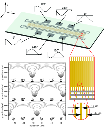
A design for trapping molecules on a microchip was first presented in 2008 by Meek et al. Meek_PhysRevLett100p153003_2008 and only minor improvements have been done ever since. The operation principle relies on the superposition of electric fields created by the electrodes on the chip. When two dipolar fields with different length scales and opposite directions are superimposed, a minimum of the electric field strength is created. The minimum is located at the point where the long-range dipole that dominates far from the surface is canceled by the short-range dipole that dominates close to the surface. Such a minimum in the electric field strength is a trap for lfs.Meek_NewJPhys11p055024_2009 A picture of the chip used by Meek et al. is shown in Fig. 1. The electrode design consists in an array of equidistant, parallel, gold electrodes, each of which is 4 mm long, 10 wide and approximately 300 nm high. They are deposited onto a 1 mm thick glass substrate with a center-to-center spacing of 40 and are coated with a 5- layer of insulating SU-8. This structure is periodically extended over about 50 mm. Each electrode is electrically connected to the electrodes that are (multiple of) six positions further, i.e. the electric field repeats itself every 240 . This geometry requires the metallization on the chip to be deposited on three different levels with insulating SU-8 layers in-between. The 4-mm long electrodes are all on the same plane, whereas the connections to the distribution buses are on different levels. When appropriate potentials are applied to the electrodes, an array of tubular electric field geometries of 4 mm length and 20 diameter are generated, on the axis of which the electric field strength drops to zero. These electric field geometries act as traps for lfs and are centered roughly 25 above the chip surface. In the bottom-left portion of the figure, the calculated contour lines of equal electric field strength above the chip are shown. The horizontal black boxes represent the section of the electrodes. The potentials applied to the electrodes are indicated directly above them. In the bottom panel, the situation is shown in which the electrodes at and create an electric field that is parallel to the axis, in the direction of negative values, for any point along the vertical line at , whereas the electrodes at and create an electric field that is pointing in the opposite direction for any point along this line. Close to the substrate, the field due to the two nearest electrodes dominates, whereas further away the field due to the next nearest electrodes is most important. It is clear, therefore, that at some point above the substrate, at a typical height on the order of the distance between adjacent electrodes, a zero of the electric field strength will be generated on the axis. At the ends of the central array in the -directions, there is a jump from a region where the potentials are on average zero to a region where the potentials are on average positive or negative (see Fig. 1). This produces an electric field along the -direction that closes the tubular traps at the two sides. However, the molecules interact only very seldom with the traps ends because of the extreme aspect ratio of these tubular traps.
Using different sets of potentials, it is also possible to position the minima either directly above an electrode (top panel), or in an intermediate position (central panel). In fact, by applying the appropriate potentials, the minima can be positioned at any -position within the 240- period, while their -position remains constant. Further, the periodic arrangement of the electrodes allows for a continuous movement of the electric field minima outside the 240- period, that is over the macroscopic distance of the whole device at a constant height of about 25 . For a given trap strength, there is a bijective relationship between the set of the applied potentials and the position of the microtraps array, so that the applied potentials must be periodic functions when the field minima travel across multiple periods. For the electrodes configuration chosen by Meek et al., the applied potentials that generate the smoothly moving traps are six approximately harmonic functions. Three of the potentials can always be positive, the other three always negative, and within each polarity set the potentials need to be phase shifted by . Since two microtraps are formed per period, as can be seen in Fig. 1, the effective periodicity is of 120 . Thus, the microtraps move at 300 m/s when the sinusoidal modulation of the potential has a frequency of 2.5 MHz. The trap depth obtained with sinusoidal modulations of 200-V amplitude peak-to-peak is of the order of 5 kV/cm. For CO molecules in the upper -doublet component of the , , state, for instance, this electric field strength corresponds to a thermal energy of about 70 mK.
Polar molecules flying parallel to the surface of the chip along the -direction can be trapped in the microtraps directly from a supersonic molecular beam. Meek_PhysRevLett100p153003_2008 The density of the molecular beam at the chip entrance determines the density of trapped molecules, which is typically in the order of 107 molecules/cm3. Initially, the frequency of the applied waveforms is chosen to match the velocity of the microtraps to that of the incoming molecules. Then, the trapped molecules can be brought to a standstill, or to any intermediate velocity, by continuously reducing the frequency of the waveforms. An acceleration of the order of 105 g can be applied, allowing to stop a supersonic beam within a few cm.
Moving away from the substrate, the contour lines run ever more parallel to the surface and the strength of the electric field decays exponentially with the -position. In the region far away from the surface, therefore, the electrode array yields a flat, repulsive mechanical potential for polar molecules in lfs states: a mirror. Indeed, an electrostatic mirror consisting of an array of parallel and equidistant electrodes on a surface to which alternating voltages are applied was first discussed by Opat et al. Opat_ApplPhysB54p396_1992 . Based on this principle, both plane Schulze_PhysRevLett93p020406_2004 and focusing GonzalezFlorez_PhysChemChemPhys13p18830_2011 microstructured mirrors for polar molecules have been realized. Moreover, Englert et al. Englert_PhysRevLett107p263003_2011 placed two such microstructured mirrors facing each other as the two faces of a capacitor to create a macroscopic (2 by 3 cm) electrostatic trap. To achieve transverse confinement of the molecules they used a high-voltage electrode between the plates that surrounds the perimeter of the trap.
Imaging experiments of the molecular beam with the focusing microstructured mirror GonzalezFlorez_PhysChemChemPhys13p18830_2011 and of trapped molecules above the chip Marx_PhysRevLett111p243007_2013 allow to estimate the effects of the charge that accumulates on the SU-8 insulating layer above the electrodes. When all electrical potential are not symmetric about ground, it was found that the mechanical potential becomes weaker toward the distribution buses that are on average further away from ground. This is interpreted as the effect of charge that accumulates on the dielectric, screening the electric field of the electrodes. Therefore, although the molecules on the chip should in principle only be sensitive to the electric field strength, the values of the applied potentials with respect to ground turn out to be also important. Moreover, the amount of trapped molecules increases with increasing amplitude of the applied potentials until about 240 V. This limit is probably an effect of the suface charges and is usually reached without damages to the microstructure.
III Non-adiabatic losses
Thus far we have been assuming that the force imposed on the molecules only depends on the gradient of the electric-field strength but not on the direction of the field itself. This is usually a good assumption, since the molecules reorient themselves and follow the new quantization axis when the field changes direction, and their potential energy changes smoothly with the strength of the field. This approximation can break down, however, when the quantum state that is used for manipulation couples to another quantum state that is close in energy. If the energy of the quantum state or the field direction changes at a rate that is fast compared to the energetic splitting, transitions between these states are likely to occur. Such transitions are particularly disastrous if lfs end up as hfs or in states that are only weakly influenced by the electric fields, as this results in a loss of the molecules from the trap. For atoms in magnetic traps, such losses are known as Majorana spin-flip transitions. Both for atoms in magnetic quadrupole traps Petrich_PhysRevLett74p3352_1995 and for polar molecules in electric quadrupole traps Kirste_PhysRevA79p051401R_2009 it has been shown that non-adiabatic losses are inversely proportional to the square of the diameter of the particle cloud. A straightforward solution to avoid Majorana transitions involves the use of an offset magnetic Fortagh_RevModPhys79p235_2007 or electric Kirste_PhysRevA79p051401R_2009 field. Due to the geometry of the molecule chip, however, applying a static offset electric field is much harder. In particular, it cannot be done without leaving the two dimensions of the present devices Meek_PhysRevA71p065402_2005 and the field generated by external electrodes perpendicular to the substrate would be strongly screened by the metallic surfaces of the microelectrodes, which are only a few microns away from the molecules. Thus other solutions must be sought.
It was demonstrated in the cases of ammonia Kirste_PhysRevA79p051401R_2009 and of carbon monoxide Meek_Science324p1699_2009 , for instance, that the choice of the appropriate isotopologue can induce a beneficial separation of the levels at zero electric field, thus reducing the non-adiabatic losses. For the simpler case of CO in the state, a degeneracy at zero field between two low-field-seeking levels and a level that is not sensitive to electric field in 12CO is lifted in 13CO due to hyperfine splitting (the 13C nucleus has a nuclear spin ), and the low-field-seeking levels never come closer than 50 MHz to the nontrappable levels. An alternative solution was demonstrated for CO and consists in the use of a magnetic field. Meek_PhysRevA83p033413_2011 If a magnetic field is applied in addition to the electric field, a splitting can be induced between the low-field-seeking and the nontrappable levels of 12CO that depends on the strength of the applied magnetic field.
The solutions mentioned in the last paragraph act on the level splitting. But the rate at which the energy of the levels changes when the molecules travel across the traps must also be considered, because it is the ratio between these two that determines the transition probability. Since the trapping potential on the molecule chip is obtained as a difference between large electric fields, it turns out to be very sensitive to imperfections in the applied waveforms. As a result, the microtraps can be jittering around much faster than the velocity of the trapped molecules with respect to the averaged trap center. Thus, improving the quality of the waveforms is a further way to reduce non-adiabatic transitions. Although this is a non-trivial task because amplitudes over 200 V between 3 MHz and DC are needed, the improvements done thus far are encouraging. A first reduction of the waveforms anharmonicity from 7% to 3% reduced the non-adiabatic losses by 10% and halved the magnitude of the magnetic field required to saturate the loss suppression. Meek_PhysRevA83p033413_2011
The suppression of non-adiabatic losses is a strong motivation to improve the quality of the waveforms. However, wide bandwith and low anharmonicity of the amplifiers that generate the waveforms turn out to be crucial for shutting down the electric field rapidly and accurately for the imaging experiments (see below). The first generation of the amplifiers is based on a AB design, realized with vacuum tubes. The second generation is a class-A design, realized with semiconductor transistors. The frequency response of each amplifier is measured and fed back to the software that calculate the waveform. The current state of the art is a total harmonic distortion below dB.
IV Addressing state transitions in trapped molecules
Molecules on a chip can be coupled to photons over a wider range of frequencies than atoms. The fundamental molecular vibrational modes can be addressed with mid-infrared photons whereas their overtones and combination modes extend into the near-infrared range. In addition, polar molecules have a dense set of rotational transitions in the sub-THz, or mm-wave, region of the spectrum. Being able to induce a transition to another internal quantum state in the molecule is particularly interesting when the molecule remains trapped in the final state as well.
Abel et al. Abel_MolecularPhysics110p1829_2012 showed an effective vibrational population transfer in molecules trapped on a chip. They coupled pulsed IR radiation around 5.9 to transfer trapped CO molecules in the state from the to the levels and addressed both Q- and R-branch transitions. Crucially, the Stark broadening of the vibrational transitions induced by the trapping fields is comparable with the laser bandwidth of about 2.5 GHz and therefore virtually all molecules could be addressed by the IR radiation. The situation is different with rotational transitions. First, rotational transitions are usually more sensitive to electric fields and the inhomogeneous broadening in the traps is larger than for vibrations. Second, sub-THz sources are typically narrow. Therefore, when rotational transitions were addressed in molecules on the chip Santambrogio_ChemPhysChem12p1799_2011 , the microtraps had to be switched off temporarily to allow for effective rotational pumping. Interestingly, molecules could be recaptured after being transferred between different rotational levels. These results thus demonstrate that mm-wavelength radiation can be coupled to CO molecules located at less than 50 above the surface of the chip—a few hundredths of the wavelength—and rotational spectra were obtained with a resolution of approximately half a MHz. An external magnetic field was used to split the Zeeman components and the resolution of the spectrum is limited by the inhomogeneities of the magnetic field above the chip induced by the metal components of the chip holder.
V Imaging molecules on the chip
The lack of closed two-level systems that makes laser cooling so hard for molecules is also responsible for the difficulties in molecular detection using absorption or laser-induced fluorescence. Moreover, in the presence of a physical structure such as a microchip, scattering or laser-induced fluorescence from surfaces adds noise to images, something which is critical when working with small samples. For these reasons, on-chip detection has only recently been demonstrated. Marx_PhysRevLett111p243007_2013 On-chip detection is based on resonance-enhanced multiphoton ionization (REMPI) Ashfold_AnnuRevPhysChem45p57_1994 , which is quantum state selective, is intrinsically background-free, and is of general applicability. REMPI is obtained on the chip by illuminating the molecules with a sheet of light parallel to the surface of the chip. It is worth noting that ions are several orders of magnitude more sensitive to electric fields than polar molecules. However, if care is taken to carefully zero all electric fields used to manipulate the neutral molecules before the ions are created, it is possible to create a spatial image of the molecules in a microchannel-plates detector. A set of magnifying ion lenses can be used to resolve the molecular distribution in individual microtraps, and since the timing of the ionizing laser can be tuned, one can follow the spatial evolution of the molecular clouds in time.
With this setup for time-resolved spatial imaging, it was possible to study the phase-space distribution of trapped molecules. The experiments are done in a similar fashion as for cold atoms: the traps are quickly turned off and a series of snapshots at different times return a movie of the ballistic expansion of the particles. In particular, this allows for a direct measurement of the temperature of the trapped molecules. Moreover, the cooling induced on the molecular ensemble by an adiabatic expansion process, induced by slowly weakening the trapping potential, can be clearly seen to lower the temperature of the molecules to about a third of the initial value (from 16 to 5 mK).Marx_PhysRevLett111p243007_2013
VI Outlook
Miniaturization yields large forces (e.g. 105 g28 amu, for CO) at the moderate electric field strenghts of a few kV/cm, with applied potentials of the order of 200 V. For comparisons, macroscopic Stark decelerators achieve accelerations about ten times lower, with electric field strenghts in the order of 100 kV/cm, and applied voltages in the 10 kV range. Microchip-based devices might thus be promising for the manipulation of heavy molecules that are typically only low-field seeking when the electric field is small. Meerakker_ChemRev112p4828_2012 ; Bulleid_PhysRevA86p021404R_2012
To confine molecular samples with a temperature of about 10 mK, the Stark broadening induced by the inhomogeneous trapping fields is in the GHz range. This precludes the application of traps in precision spectroscopy and collision experiments. For molecule-based spectroscopic measurements, the shot-noise limit on the statistical error is proportional to , where is the time each molecule spends in the light field and is the total number of molecules that participate in the experiment. Moreover, the major sources of systematic errors and uncertainties in molecular spectroscopy are the presence of stray fields and Doppler broadening. These two issues are usually approached by keeping the size of the experimental apparatus small, reducing the magnitude of all necessary fields, and by employing Doppler-free techniques, like for instance two photons spectroscopy. Therefore, the use of a microchip to produce a slow beam of cold molecules for spectroscopy is not necessarily as inconvenient as it might seem at a first glance. First, the density of trapped and decelerated molecules on the microchip is the same as for macroscopic devices or for free molecular beams—only the absolute number of molecules is small. Since a minimum of electric field is required for a population transfer to be measurable, the large laser beam waists that would take advantage of a larger number of molecules are often unavailable in two-photon experiments. Second, miniaturization of the decelerator helps in reducing the magnitude of stray fields. Finally, miniaturization can be convenient in the case of a Ramsey-configuration experiment, where mechanical stability to the interferometric level is needed.
Acknowledgements.
I gratefully acknowledge the fruitful discussion with Samuel A. Meek.References
- (1) R. Daw and J. Finkelstein, Nature 442 (2006), 367.
- (2) H. C. Morris, M. Damon, J. Maule, L. A. Monaco, and N. Wainwright, Astrobiology 12 (2012), 830.
- (3) T. Frisk, D. Ronnholm, W. van der Wijngaart, and G. Stemme, Lab Chip 6 (2006), 1504.
- (4) N. Heine and K. R. Asmis, Int. Rev. Phys. Chem. 34 (2015), 1.
- (5) K. R. Asmis and D. M. Neumark, Acc. Chem. Res. 45 (2012), 43.
- (6) C. J. Johnson, J. A. Fournier, C. T. Wolke, and M. A. Johnson, J. Chem. Phys. 139 (2013), 224305.
- (7) J. A. Fournier, C. J. Johnson, C. T. Wolke, G. H. Weddle, A. B. Wolk, and M. A. Johnson, Science 344 (2014), 1009.
- (8) L. Jiang, T. Wende, P. Claes, S. Bhattacharyya, M. Sierka, G. Meijer, P. Lievens, J. Sauer, and K. R. Asmis, J. Phys. Chem. A 115 (2011), 11187.
- (9) E. Janssens, G. Santambrogio, M. Brümmer, L. Wöste, P. Lievens, J. Sauer, G. Meijer, and K. R. Asmis, Phys. Rev. Lett. 96 (2006), 233401.
- (10) H. J. Metcalf and P. van der Straten, Laser cooling and trapping, Springer, Berlin, 1999.
- (11) J. Fortágh and C. Zimmermann, Rev. Mod. Phys. 79 (2007), 235.
- (12) W. Hänsel, P. Hommelhoff, T. W. Hänsch, and J. Reichel, Nature 413 (2001), 498.
- (13) T. Schumm, S. Hofferberth, L. M. Andersson, S. Wildermuth, S. Groth, I. Bar-Joseph, J. Schmiedmayer, and P. Krüger, Nat. Physics 1 (2005), 57.
- (14) T. van Zoest, N. Gaaloul, Y. Singh, H. Ahlers, W. Herr, S. T. Seidel, W. Ertmer, E. Rasel M. Eckart, E. Kajari, S. Arnold, G. Nandi, W. P. Schleich, R. Walser, A. Vogel, K. Sengstock, K. Bongs, W. Lewoczko-Adamczyk, M. Schiemangk, T. Schuldt, A. Peters, T. Koönemann, H. Müntinga, C. Lämmerzahl, H. Dittus, T. Steinmetz, T. W. Hänsch, and J. Reichel, Science 328 (2010), 1540.
- (15) C. Ospelkaus, U. Warring, Y. Colombe, K. R. Brown, J. M. Amini, D. Leibfried, and D. J. Wineland, Nature 476 (2011), 181.
- (16) M. Gring, M. Kuhnert, T. Langen, T. Kitagawa, B. Rauer, M. Schreitl, I. Mazets, D. Adu Smith, E. Demler, and J. Schmiedmayer, Science 337 (2012), 1318.
- (17) J Baron, W. C Campbell, D Demille, J. M Doyle, G Gabrielse, Y. V Gurevich, P. W Hess, N. R Hutzler, E Kirilov, I Kozyryev, B. R O’leary, C. D Panda, M. F Parsons, E. S Petrik, B Spaun, A. C Vutha, and A. D West, Science 343 (2014), 269.
- (18) C. Daussy, T. Marrel, A. Amy-Klein, C. T. Nguyen, C. J. Bordé, and C. Chardonnet, Phys. Rev. Lett. 83 (1999), 1554.
- (19) E. J. Salumbides, J. C. J. Koelemeij, J. Komasa, K. Pachucki, K. S. E. Eikema, and W. Ubachs, Phys. Rev. D 87 (2013), 112008.
- (20) E. J. Salumbides, G. D. Dickenson, T. I. Ivanov, and W. Ubachs, Phys. Rev. Lett. 107 (2011), 043005.
- (21) C. Daussy, M. Guinet, A. Amy-Klein, K. Djerroud, Y. Hermier, S. Briaudeau, C. J. Bordé, and C. Chardonnet, Phys. Rev. Lett. 98 (2007), 250801.
- (22) A. Shelkovnikov, R. Butcher, C. Chardonnet, and A. Amy-Klein, Phys. Rev. Lett. 100 (2008), 150801.
- (23) S. Truppe, R.J. Hendricks, S.K. Tokunaga, H.J. Lewandowski, M.G. Kozlov, C. Henkel, E.A. Hinds, and M.R. Tarbutt, Nature Comm. 4 (2013), 2600.
- (24) J. Bagdonaite, P. Jansen, C. Henkel, H. L. Bethlem, K. M. Menten, and W. Ubachs, Science 339 (2013), 46.
- (25) E. J. Salumbides, D. Bailly, A. Khramov, A. L. Wolf, K. S. E. Eikema, M. Vervloet, and W. Ubachs, Phys. Rev. Lett. 101 (2008), 223001.
- (26) D. DeMille, Phys. Rev. Lett. 88 (2002), 067901.
- (27) A. André, D. DeMille, J. M. Doyle, M. D. Lukin, S. E. Maxwell, P. Rabl, R. J. Schoelkopf, and P. Zoller, Nat. Phys 2 (2006), 636.
- (28) K. Góral, L. Santos, and M. Lewenstein, Phys. Rev. Lett. 88 (2002), 170406.
- (29) A. Micheli, G. K. Brennen, and P. Zoller, Nature Phys. 2 (2006), 341.
- (30) R. V. Krems, Phys. Chem. Chem. Phys. 10 (2008), 4079.
- (31) M. H. G. de Miranda, A. Chotia, B. Neyenhuis, D. Wang, G. Quéméner, S. Ospelkaus, J. L. Bohn, J. Ye, and D. S. Jin, Nature Phys. 7 (2011), 502.
- (32) A. V. Avdeenkov and J. L. Bohn, Phys. Rev. A 66 (2002), 052718.
- (33) T. V. Tscherbul and R. V. Krems, J. Chem. Phys. 129 (2008), 034112.
- (34) E. S. Shuman, J. F. Barry, and D. DeMille, Nature 467 (2010), 820.
- (35) J. F. Barry, E. S. Shuman, E. B. Norrgard, and D. DeMille, Phys. Rev. Lett. 108 (2012), 103002.
- (36) V. Zhelyazkova, A. Cournol, T. E. Wall, A. Matsushima, J. J. Hudson, E. A. Hinds, M. R. Tarbutt, and B. E. Sauer, Phys. Rev. A 89 (2014), 053416.
- (37) J. D. Weinstein, R. deCarvalho, T. Guillet, B. Friedrich, and J. M. Doyle, Nature 395 (1998), 148.
- (38) S. A. Meek, H. Conrad, and G. Meijer, New J. Phys. 11 (2009), 055024.
- (39) S. A. Meek, H. L. Bethlem, H. Conrad, and G. Meijer, Phys. Rev. Lett. 100 (2008), 153003.
- (40) H. L. Bethlem, G. Berden, F. M. H. Crompvoets, R. T. Jongma, A. J. A. van Roij, and G. Meijer, Nature 406 (2000), 491.
- (41) T. Rieger, T. Junglen, S. Rangwala, P. W. H. Pinkse, and G. Rempe, Phys. Rev. Lett. 95 (2005), 173002.
- (42) H. L. Bethlem and G. Meijer, Int. Rev. Phys. Chem. 22 (2003), 73.
- (43) S. Y. T. van de Meerakker, HL Bethlem, N Vanhaecke, and G Meijer, Chem. Rev. 112 (2012), 4828.
- (44) G. I. Opat, S. J. Wark, and A. Cimmino, Appl. Phys. B 54 (1992), 396.
- (45) S. A. Schulze, H. L. Bethlem, J. van Veldhoven, J. Küpper, H. Conrad, and G. Meijer, Phys. Rev. Lett. 93 (2004), 020406.
- (46) A. I. González Flórez, S. A. Meek, H. Haak, H. Conrad, G. Santambrogio, and G. Meijer, Phys. Chem. Chem. Phys. 13 (2011), 18830.
- (47) B. G. U. Englert, M. Mielenz, C. Sommer, J. Bayerl, M. Motsch, P. W. H. Pinkse, G. Rempe, and M. Zeppenfeld, Phys. Rev. Lett. 107 (2011), 263003.
- (48) S. Marx, D. Adu Smith, M. J. Abel, T. Zehentbauer, G. Meijer, and G. Santambrogio, Phys. Rev. Lett. 111 (2013), 243007.
- (49) W. Petrich, M. H. Anderson, J. R. Ensher, and E. A. Cornell, Phys. Rev. Lett. 74 (1995), 3352.
- (50) M. Kirste, B. G. Sartakov, M. Schnell, and G. Meijer, Phys. Rev. A 79 (2009), 051401(R).
- (51) S. A. Meek, E. R. I. Abraham, and N. E. Shafer-Ray, Phys. Rev. A 71 (2005), 065402.
- (52) S. A. Meek, H. Conrad, and G. Meijer, Science 324 (2009), 1699.
- (53) S. A. Meek, G. Santambrogio, B. Sartakov, H. Conrad, and G. Meijer, Phys. Rev. A 83 (2011), 033413.
- (54) M. J. Abel, S. Marx, G. Meijer, and G. Santambrogio, Molecular Physics 110 (2012), 1829.
- (55) G. Santambrogio, S. A Meek, M. J. Abel, L. M. Duffy, and G. Meijer, ChemPhysChem 12 (2011), 1799.
- (56) M. N. R. Ashfold and J. D. Howe, Annu. Rev. Phys. Chem. 45 (1994), 57.
- (57) N. E. Bulleid, R. J. Hendricks, E. A. Hinds, S. A. Meek, G. Meijer, A. Osterwalder, and M. R. Tarbutt, Phys. Rev. A 86 (2012), 021404R.