Supplemental Material for ”Shot Noise of a Quantum Dot Measured with Gigahertz Impedance Matching”
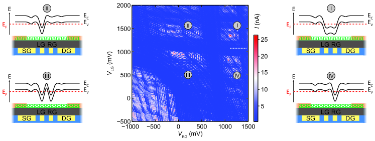
Quantum dot formation. The dc current on a large range of left gate (LG) and right gate (RG) voltages is plotted in the main figure of Fig. S1. The source gate (SG) as well as the drain gate (DG) are fixed at V to get p-doped leads. The valence and conduction band edges with respect to the Fermi level are depicted for four different regimes I-IV, which are separated by a band-gap transition. With the help of the two central gates (LG, RG), one can get a single quantum dot (QD) in the centre (I), a QD above the LG (II), a QD above the RG (IV) or a triple QD (III). It is best seen in the left bottom corner, where the entire CNT should be p-doped, that Fermi-level pinning close to the leads can still lead to a QD formation. For the measurements presented in the main text, we concentrate on the single QD regime (I). If plotted with a different color bar, weaker resonance lines would still appear in the figure at the white dashed line, where the left gate is set to mV. Since the couplings to source and drain are weak enough to get a good confinement for clearly visible QDs in this regime, this is chosen to be the working regime for all measurements in the main text.
The excited state spacing in this single QD regime can be deduced from Fig. 3 in the main text and results in about 8 meV. It can be compared with the single-particle level spacing Nygard et al. (1999). The obtained QD length is nm, meaning that the QD is located mainly between the two central gates, which are separated by 100 nm.
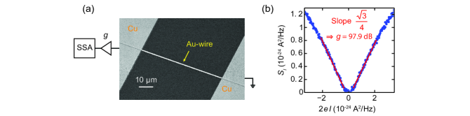
Setup calibration. For the calibration of the setup, the sample is replaced by a metal wire with a well-known noise emission [see Fig. S2(a)]. The gold wire is 30 nm-thick and 680 nm-wide with a residual resistance of 39 . It is connected to two 500 nm-thick copper pads of the size , acting as heat sinks. At the base temperature of 20 mK, the wire length of 50 m is between the inelastic electron scattering length of about 20 m and the electron-phonon interaction length of approximately 580 m Henny (1998). Therefore, the wire is in the hot-electron regime, where electrons get heated inside the wire. The current noise is measured with a signal and spectrum analyser (SSA) at the same center frequency GHz and with the same bandwidth MHz as used for all the data in the main text.
Fig. S2(b) shows the shot noise dependence on current. The current noise spectral density is derived from the integrated noise power by subtracting the background noise at zero bias , dividing by the BW and taking into account the voltage division between the sample with resistance and the detection line with impedance (see eq. S12 and eq. S15):
| (S1) |
The setup gain contains the amplifier gain of the cryogenic and the room-temperature amplifiers and the setup attenuation. It is determined in the following way: is the slope of the detected, amplified noise in the linear regime (red dotted line) divided by the well-established Fano factor of a wire in the hot-electron regime of Steinbach et al. (1996). The Fano factor decrease at high bias voltage is due to electron cooling via phonons.
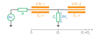
Transmission function of a stub tuner. Coplanar transmission lines (CTLs) are characterized by their characteristic impedance and their complex propagation constant . The real part of the propagation constant is the damping per length and the imaginary part the frequency-dependent wavenumber with the effective dielectric constant . A stub tuner is made out of two CTLs connected in parallel, as sketched in Fig. S3. One of the CTLs with the length is terminated by the device with differential resistance , whereas the other CTL with the length is open-ended.
For the voltages in both CTL arms (CTL 1 and CTL 2), a wave function Ansatz is taken:
| (S2) | ||||
where and () are the coefficients for right-moving waves and left-moving waves, respectively. With the definition of the characteristic impedance , one can write the current in the CTLs as
| (S3) | ||||
To determine the four coefficients and , four boundary conditions are needed. First, we require that the current at the open end vanishes,
| (S4) |
The voltage on the other end is set by Ohm’s law to
| (S5) |
Furthermore, the voltage has to be continuous at the connection of the two arms,
| (S6) |
At last, Kirchhoff’s law applies at the junction between the two arms:
| (S7) |
What remains is a rather lengthy calculation to find the coefficients, which are used to evaluate the transmission function defined as
| (S8) |
Eventually, the voltage-transmission function of a stub tuner is found to be
| (S9) |
where the reflection coefficient . Around the resonance frequency , the stub tuner has a window of high transmission. In the lossless case () and if , the condition for matching is Pozar (2005). If in addition only frequencies around are considered ( with ), the magnitude square of the transmission function can be approximated to
| (S10) |
The stub tuner bandwidth defined as full width at half maximum (FWHM) is in this ideal case
| (S11) |
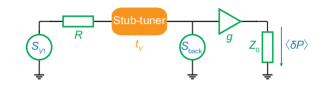
Signal-to-noise ratio. Given the transmission function of the stub tuner, one can quantify how much noise power arrives at the detection line. Fig. S4 shows a schematic of the situation. We assume the sample to emit a frequency-independent current noise spectral density . Thus the voltage noise in front of the stub tuner is . The sum of the voltage noise integrated over the measurement bandwidth after passing the stub tuner and the amplifier with power gain is . Finally, the noise power measured over a resistance of is . Putting everything together results in the measured noise power
| (S12) |
This is eq. 4 in the main text without taking the background noise into account yet.
While the general integration of the stub tuner transmission function (eq. S9) has to be done numerically, an analytical expression exists for the integral of the lossless transmission function at matching (eq. S10):
| (S13) |
It defines an upper bound for the detectable noise power with a stub tuner, which is
| (S14) |
This transmitted noise power has to be compared with the signal measured in the absence of impedance matching. The noise spectral density is small in this case, but one can integrate over a large bandwidth. On the other hand, the bandwidth is always restricted by other components. In our setup, the circulator has the smallest bandwidth of MHz. Eq. S12 can be generally used to get the signal power for this kind of setup by taking the appropriate transmission function . If there is no impedance-matching circuit at all, the stub tuner is replaced by an element with a constant transmission function obtained via eq. S9 by setting . It leads to the same result as if voltage division of the emitted noise voltage is considered in the circuit drawn in Fig. S4. By means of eq. S12, the resulting noise power measured without impedance matching is then
| (S15) |
Therefore, the maximum enhancement in detectable noise power obtained with a lossless stub tuner at full matching at a resonance frequency GHz is .
So far the discussion was about the noise signal only. But the main advantage of a matching circuit is revealed by considering the signal-to-noise ratio (SNR). Noise is in this context the background noise, as for instance the amplifier noise. Its power spectral density is assumed to be frequency independent. If one assumes the background noise source to be introduced between the impedance-matching circuit and the amplifier (see Fig. S4), the background noise power picked up over the measurement bandwidth (BW) is . This leads to the general expression for the SNR
| (S16) |
where eq. S12 is used to get the last expression. Without impedance matching, one can use eq. S15 and gets
| (S17) |
Eventually, we want to compare the SNRs with and without impedance matching. To do so, we introduce the figure of merit for impedance matching as
| (S18) |
This means that depends on the transmission function of the resonant circuit and the chosen integration bandwidth BW, which is optimally the FWHM given in eq. S11. An upper bound for considering a lossless stub tuner at full matching can then be given with the help of eq. S13:
| (S19) |
which amounts to a factor as high as for k. For realistic matching circuits, the integration of the general transmission function (eq. S9) can be done numerically. Using the stub-parameters from the main text derived by reflectometry, the resulting improvement in the SNR is still at this resistance if the bandwidth is the FWHM, although the circuit is not fully matched to k.
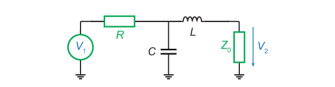
Comparison with -circuit In the last part, we compare this result with an matching circuit. To this end, an expression for the voltage-transmission function appearing in eq. S18 has to be derived. Using the circuit drawn in Fig. S5, the transmission function is determined to be
| (S20) |
at matching, when . Here . In the limit where and , can be approximated and its magnitude squared reads
| (S21) |
The FWHM of this resonance function is . It scales with whereas the bandwidth of the stub tuner scales with (eq. S11), leading at high resistances to a much larger BW for an circuit compared with a stub tuner. Furthermore, the integral of the transmission function in eq. S21 can be evaluated analytically:
| (S22) |
What remains is to plug and the integrated transmission function into eq. S18 in order to get the maximum figure of merit for a lossless, fully matched network:
| (S23) |
It is exactly the same result as for the stub tuner (eq. S19). This is not surprising since with any matching circuit, the transmission maximum is fixed to and only the BW can be modified. Still, the large bandwidth of an matching circuit can be beneficial for some measurements, for example a fast, time-resolved read-out. But the gain in the SNR remains the same, since the increase in integration bandwidth also leads to an enhanced background noise.
In conclusion, an impedance-matching circuit leads to a significant increase in the figure of merit. The discussion here concentrates on the improvement of the SNR with impedance matching. But we want to note that it is equally important to minimize the background noise in the first place. By looking at eq. S16, it gets evident that apart from impedance matching to achieve a high signal transmission and properly choosing the right BW, the only way to increase the SNR is to reduce , for instance with Josephson parametric amplifiers. On the other hand, the SNR is not the only limiting characteristic of an experiment. What counts experimentally is to reach a certain SNR which is high enough for the intended accuracy. Any further increase of the SNR does not reveal new features. But the larger the figure of merit is, the smaller is the measurement time needed to reach the same SNR.
References
- Nygard et al. (1999) J. Nygard, D.H. Cobden, M. Bockrath, P.L. McEuen, and P.E. Lindelof, “Electrical transport measurements on single-walled carbon nanotubes,” Applied Physics A 69, 297–304 (1999).
- Henny (1998) M. Henny, Ph.D. thesis, University of Basel (1998), p. 57.
- Steinbach et al. (1996) Andrew H. Steinbach, John M. Martinis, and Michel H. Devoret, “Observation of hot-electron shot noise in a metallic resistor,” Phys. Rev. Lett. 76, 3806–3809 (1996).
- Pozar (2005) D.M. Pozar, “Microwave engineering,” (John Wiley & Sons Inc., Hoboken, 2005) Chap. 5, p. 232, 3rd ed.