Electron transport of WS2 transistors in a hexagonal boron nitride dielectric environment
Abstract
We present the first study of the intrinsic electrical properties of WS2 transistors fabricated with two different dielectric environments WS2 on SiO2 and WS2 on h-BN/SiO2, respectively. A comparative analysis of the electrical characteristics of multiple transistors fabricated from natural and synthetic WS2 with various thicknesses from single- up to four-layers and over a wide temperature range from 300K down to 4.2 K shows that disorder intrinsic to WS2 is currently the limiting factor of the electrical properties of this material. These results shed light on the role played by extrinsic factors such as charge traps in the oxide dielectric thought to be the cause for the commonly observed small values of charge carrier mobility in transition metal dichalcogenides.
Introduction
The emerging class of atomically thin semiconducting materials formed by transition metal dichalogenides (TMDCs) is showing a plethora of complementary properties to those of graphene that are of interest to fundamental and applied research. These materials are uniquely suited to study the superconducting phase transition in the extreme two-dimensional limit inherent to atomically thin systems Novoselov2005 ; Ayari2007 ; Taniguchi2012 ; Bao2013 . At the same time TMDCs have a band gap which is essential for transistor applications and which could enable a new class of atomically thin photo-transistors. For example WS2 has a direct band gap of 2 eV in single layer form Band1 ; gap1 ; gap2 ; Gutierrez and has already shown great promise as a flexible transistor with field effect mobilities comparable to the best liquid crystals and on/off ratio of the current exceeding 106 liquid . Understanding the limiting factors of the electrical properties of TMDCs is an open quest and a stepping stone for accessing novel physics in these systems.
The typical values of charge carrier mobility measured in thin WS2 flakes are always much lower than those measured in bulk material Ayari2007 ; Bao2013 . This behaviour has been interpreted as due to defect states in the SiO2 substrate leading to the localization of charge carriers in TMDCs and a small charge carrier mobility impurity . To probe the intrinsic electrical properties of TMDCs it would be necessary to measure electrical transport in either suspended structures or in transistors fabricated on clean substrates with fewer impurities than typically present in SiO2. An ideal choice for such a substrate is hexagonal boron nitride hBN , which is a preferred substrate for high quality graphene transistors since it has a very low concentration of charge scattering impurities and is atomically flat highMob . To date such a study has not yet been conducted and the consequent lack of knowledge is limiting the potential impact of TMDCs on fundamental and applied research. Furthermore most of the studies conducted so far have been limited to just MoS2, while other TMDCs such as WS2 have not yet received much attention, whereas they might be better suited than MoS2 for a given application.
Here we present the first study of the electrical properties in WS2 transistors fabricated on different dielectrics (i.e. SiO2 and h-BN/SiO2) and using synthetic as well as natural WS2. The comparative analysis of the electrical characteristics of these transistors studied in the temperature range from 300K down to 4.2 K shows that in all cases electrical transport takes place via hopping conduction through localized states shklov ; Efros . At low temperature (T20K) we observe peaks of the conductance as a function of back-gate voltage and source-drain bias due to inelastic tunnelling in the impurity states with sub-gap energy. These results show that intrinsic disorder rather than extrinsic factors such as defect states in the oxide dielectric is limiting the electrical properties of WS2 and more generally TMDCs.
Results
Thin flakes of WS2 were obtained by mechanical exfoliation of flakes from synthetic crystals onto p-doped Si/SiO2 substrate that serves as a back gate (for natural WS2 see supporting information). Thin flakes are first identified with the aid of optical microscopy and their thickness is subsequently determined by atomic force microscopy (AFM) and Raman spectroscopy. The fabrication of WS2 transistors on h-BN and subsequent encapsulation in h-BN is carried out using the dry transfer method first developed for graphene highMob . This consists of exfoliating WS2 onto a substrate coated by water soluble polymer and PMMA. After dissolving in water the soluble polymer, the free WS2/PMMA bilayer is aligned onto previously exfoliated h-BN ( 20 nm thick) on p-doped Si/SiO2. The substrate is then heated up to melt the PMMA and secure contact between WS2 and h-BN and the PMMA is subsequently removed in acetone. Electrical contacts to WS2 are fabricated using standard electron beam lithography, thermal evaporation and lift-off of Cr/Au (5/70 nm).
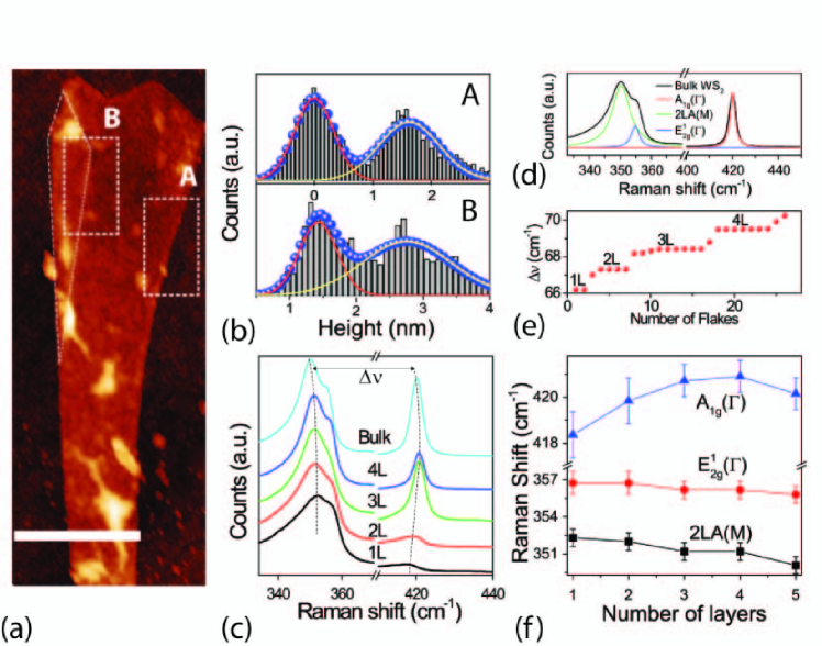
Figure 1a shows an AFM measurement of a thin WS2 flake with a fold in the upper left corner highlighted by a dashed line. A statistical study of the height measured in areas which include the step edge at WS2/SiO2 (region A) and the folded corner (region B) shows a comparable step height of nm in A and nm in B, see Figure 1b. Since the thickness of a monolayer WS2 flake is nm Ramanws3 ; Gutierrez we conclude that this flake is a bilayer. A comparative plot of the Raman spectra (see methods) for WS2 with different layer numbers shows marked differences depending on the specific thickness of the flake, see Figure 1c. More specifically it is known that the peak with low Raman shift ( cm-1) is a convolution of two Lorentzians (Figure 1d) whose positions change as a function of the layer number Ramanws2 . One Lorentzian is due to the second order longitudinal acoustic phonon mode (2LA(M)) corresponding to collective oscillations of the atoms in the plane, and this gives a Raman peak at 352.7 cm-1 in single layer WS2. The second Lorentzian is given by the in-plane optical phonon mode (E()) representing the in-plane counter oscillations of W and S atoms in the lattice. Finally the out-of-plane optical phonon mode (A1g()) representing the out-of-plane oscillations of W and S atoms gives a Raman peak at 416.6cm-1. A plot of the relative wavenumber shift ( that is the difference between the 2LA(M) and A1g()Raman peaks) for a large number of flakes with various thicknesses shows that changes in a discrete way according to the number of layers which have been independtly measured with AFM, see Fig. 1e. Finally, upon increasing the number of WS2 layers the position of the 2LA(M) and E() peaks redshift monotonously, whereas the A1g() peak blue shifts as previously shown Ramanws2 , see Figure 1f.

Having established a reliable procedure to identify the layer number of WS2 flakes we now turn to investigate the electrical transport properties of this material. The source-drain current vs. bias voltage characteristics (I-V) of WS2 transistor devices are always highly non-linear and upon performing current-bias annealing, a linear I-V around zero voltage bias is attained (see Figure 2a and supplementary information). Owing to the difference in work function between WS2 and Cr, a Schottky barrier of about 100meV has to be expected at this interface when no-gate voltage is applied. The observed bias-annealing changes in the I-V and the large values of voltage bias at which these non-linearity occur suggest a different origin for this phenomenon, that is the possible presence of an oxide barrier at the WS2/Cr interface which can be electrically broken upon applying a large voltage bias as shown in Figure 2a. In the following we only consider the analysis of electrical transport measurements in devices after bias-annealing.
Figure 2b-d show the room temperature field effect transistor (FET) transfer characteristics, that is the gate voltage (Vg) dependence of the conductivity (), for monolayer WS2 on SiO2 (Figure2b), four-layer WS2 sample on a SiO2 (Figure2c) and four-layer WS2 sample on a h-BN/SiO2 (Figure2d). In all cases we observe that the conductivity has a large on-off ratio typical of semiconducting materials, with a finite threshold voltage. However we find that the field effect mobility () is always larger in WS2 on h-BN than in WS2 on SiO2 (0.23 cm2V-1s-1 for 1L-WS2/SiO2, 17 cm2V-1s-1 for 4L-WS2/SiO2 and 80 cm2V-1s-1 for 4L-WS2/h-BN/SiO2 in Figure 2(b-d)). A large hysteresis is also present in for WS2 on SiO2 but is fully suppressed when WS2 is on h-BN/SiO2. Similar hysteresis in I-V have also been reported in graphene and is commonly attributed to dopants present in the SiO2 dielectric SiO2surface ; grapheneHyst .

Discussion
For all the measured devices we find that the temperature dependence of shows a pronounced suppression of the value of upon lowering the temperature as expected for a semiconducting material, see Figure 3a. In these devices we apply a large enough value of gate voltage such that the charge carriers are directly injected from the metal contacts into the conduction band of WS2. In this limit the relevant energy scale dominating the temperature dependence of the zero-bias resistance is the difference between the Fermi energy and the conduction band edge of the n-doped semiconductor (i.e. WS2) Das2013 . A plot of as a function of T-1 at reveals that from 260K down to 100K the conduction takes place by thermally activated charge carriers, i.e. with the activation energy and the Boltzman constant. The values of estimated from a fit of for 50VV are in the range 0.109eV0.113eV and change linearly with , see inset in Figure 3b. These values of are compatible with the voltage bias range over which non-linear I-V are measured (see blue curve in Figure 2a) suggesting that is the energy from the Fermi level to the conduction band edge (), i.e. which is also much larger than the Schottky barrier height ( 100 meV).
The smooth dependence of on demonstrates that for sub-gap energies the Fermi level can be continuously tuned by means of a gate voltage throughout the defect induced states. To estimate the density of defect states we consider the equivalent gate capacitance of these WS2 transistors that is the series of the gate oxide capacitance () and defect states capacitance (), i.e. Ayari2007 . Knowing that the oxide capacitance per unit area is Fm-2 we find , where q is the unit of charge and D(E) is the density of defect states which we estimate to be J-1m-2 .

The dominant role of disorder induced states with sub-gap energies becomes fully apparent when considering a fit of the low temperature in logharitmic scale in terms of with critical exponent, see Figure 3c. This study reveals that p=1/3 gives the best fit stemming for non-interacting Mott variable range hopping shklov ; Efros ; Alex where is the hopping parameter and is related to the density of localised states existing within the forbidden gap and the electron wavefunction size by the following relation . The extracted values for the hopping parameter at each different gate voltage are plotted in figure 3(d) along with the conductance at T = 4.2 K. This comparative plot shows a clear correlation between the hopping parameter and the conductance whereby peaks in conductance correspond to very low values of . Furthermore is found to fluctuate from K to K in a small gate range (from to 52V, corresponding to an energy window of just 0.25meV). Consequently the estimated localization radius in WS2 increases from 1.8 nm to 17 nm. These observations indicate that the sub-gap impurities states have peaks of narrow energy band-widths dominating electrical transport for sub-gap energies.
Another prominent feature evident in the temperature dependence of is the emergence of peaks for T100K with decreasing amplitude for T20K, see Figure 3a. At the same time the differential conductance as a function of source-drain bias and gate voltage at T4.2K (Figure 4a) shows that these peaks shift their position as a function of voltage bias. These observations suggest that charge transport at sub-gap energies occurs through inhomogeneous charge puddles and localized states in WS2. Since we observe a similar behaviour in a variety of samples independently of (1) the WS2 flakes aspect ratio, (2) the WS2 layer number and (3) the dielectric environment (WS2/BN/SiO2, see supplementary information) we conclude that the localized states dominating electrical transport in WS2 at sub-gap energies are intrinsic to the WS2 and not extrinsic such as defect states in the dielectric.
To estimate the localization radius () we consider electrical transport measurements of a representative 4L-WS2 in which the peaks of are spaced by an average gate voltage V corresponding to 0.17 meV, see bottom graph in Figure 4. In this device the peaks of at fixed as a function of source-drain bias () are spaced by an average source-drain bias mV. Since the threshold voltage bias needed to observe electrical conduction is mV and the sample has a length of 350 nm the threshold electric field is V/m. This value of together with the observed average peak separation of 0.17 meV gives a localization region of diameter nm which is consistent with the extracted value of the localization radius from the analysis conducted on the temperature dependence of .
Finally we note that Coulomb blockade cannot account for the observed peaks of . Indeed, if we assume a charging energy in our devices of Ec 40 - 50 meV estimated directly from the stability diagram shown in Figure 4, we extract a diameter d Ec 20 - 40 nm for the confining regions (C, and with the dielectric constant for vacuum and BN and ). Given the dimensions of the conductive WS2 channel, our devices would consist of 100-1000 charging regions (i.e. (length width)/d = (350 nm 1500 nm)/d). The stability diagram of such an array of charging islands would consist of many overlapping Coulomb diamonds which are not observed in our measurements. An indication of the underlying physical process originating these peaks of is given by the temperature dependence of presented in Figure 3a: we alwasy observe that the amplitude of the peaks decreases upon lowering the temperature. This behaviour has been previously reported in other semiconducting systems Yakimov ; Savchenko and it is a fingerprint of inelastic tunnelling which in WS2 occurs through the sub-gap impurity states.
In summary we have presented the first systematic study of the intrinsic electrical properties of thin WS2 flakes. By comparing the I-V of transistors fabricated using two different dielectric environments (i.e. (1) WS2 on SiO2 and (2) WS2 on h-BN/SiO2) we find that hopping through localized states dominate electrical transport over a wide temperature range (T100K). This intrinsic disorder has a finite density of states at sub-gap energies which contribute with inelastic tunnelling to electrical transport. These results demonstrate the dominant role played by intrinsic disorder over extrinsic factors such as defect states in the oxide dielectric as a limiting factor of the electrical properties of WS2.
Methods
Materials: Synthetic WS2 was purchased from Lowerfriction.com.
Measurement techniques: The Raman spectra where measured with a Renishaw spectrometer using an excitation laser with a wavelength of 532 nm, focused to a spot size of 1.5 m diameter and
1 mW incidente power. These measurements were performed in air and at room temperature.
Electrical measurements: The electrical transport measurements were performed in constant voltage configuration with excitation voltage smaller than kBT, with kB Boltzmann constant. The differential conductance was measured using the lock-in technique.
Acknowledgments
F.W. acknowledges Gunnar Färber (mineralien@online.de) for providing a specimen of natural tungstenite.
S.R. and M.F.C. acknowledge financial support from EPSRC (Grant no. EP/J000396/1 and no. EP/K010050/1) and from the Royal Society Travel Exchange Grant 2012 and 2013.
Author contribution statement
F.W. conducted the fabrication and electrical measurements. T.H.B. conducted the AFM measurements. D.C.H. participated in the electrical measurements. F.W., S.R. and M.F.C. interpreted the data and wrote the manuscript. All authors reviewed the manuscript.
Additional information
Competing financial interests: The authors declare no competing financial interests.
License: This work is licensed under a Creative Commons
Attribution-NonCommercial-NoDerivs 3.0 Unported License. To view a copy of this
license, visit http://creativecommons.org/licenses/by-nc-nd/3.0/
References
- (1) Novoselov, K.S., et al. Two-dimensional atomic crystals. P. Natl. Acad. Sci. USA 102, 10451-10453 (2005).
- (2) Ayari, A., Cobas, E., Ogundadegbe O. Fuhrer, M.S. Fabrication and electrical characterization of ultrathin crystals of layered transition-metal dichalcogenides. J. App. Phys. 101, 014507 (2007).
- (3) Taniguchi, K., Matsumoto, A., Shimotani H. Takagi, H. Electric-field-induced superconductivity at 9.4 K in a layered transition metal disulphide MoS2. App. Phys. Lett. 101, 042603 (2012).
- (4) Bao, W., Cai, X., Kim, D., Sridhara, K. Fuhrer, M.S. High mobility ambipolar MoS2 field-effect transistors: Substrate and dielectric effects. App. Phys. Lett. 102, 042104 (2013).
- (5) Mattheiss, L.F. Band Structures of Transition-Metal-Dichalcogenide Layer Compounds. Phys. Rev. B 8, 3719-3740 (1973).
- (6) Frey, G.L., Elani, S., Homyonfer, M., Feldman, Y. Tenne, R. Optical-absorption spectra of inorganic fullerenelike MS2 (M=Mo, W). Phys. Rev. B 57, 6666-6671 (1998).
- (7) Mak, K.F., Lee, C., Hone, J., Shan, J. Heinz, T.F. Atomically Thin MoS2: A New Direct-Gap Semiconductor. Phys. Rev. Lett. 105, 136805 (2010).
- (8) Gutiérrez, H.R., et al. Extraordinary Room-Temperature Photoluminescence in Triangular WS2 Monolayers. Nano Lett. 13, 3447-3454 (2013).
- (9) McCulloch, I., et al. Liquid-crystalline semiconducting polymers with high charge-carrier mobility. Nat. Mater. 5, 328-333 (2006).
- (10) Ghatak, S., Pal A.N. Ghosh, A. Nature of Electronic States in Atomically Thin MoS2 Field-Effect Transistors. ACS Nano 5, 7707-7712 (2011).
- (11) Lee, G.-H., et al. Electron tunneling through atomically flat and ultrathin hexagonal boron nitride.App. Phys. Lett. 99, 243114 (2011).
- (12) Dean, C.R., et al. Boron nitride substrates for high-quality graphene electronics. Nat. Nanotechnol. 5, 722-726 (2010).
- (13) Shklovskii, B.I. Efros, A.L. eds., Electronic Properties of Doped Semiconductors ACS (Springer Series in Solid State Sciences, Vol. 45, Berlin, 1984).
- (14) Efros, A.L. Shklovskii, B.I. eds., Electron-Electron Interactions in Disordered Systems (North-Holland, Amsterdam, 1985)
- (15) Ramakrishna, M.H.S.S., et al. MoS2 and WS2 Analogues of Graphene. Angew. Chem. Int. Edit. 49, 4059-4062 (2010).
- (16) Berkdemir, A., et al. Identification of individual and few layers of WS2 using Raman Spectroscopy. Sci. Rep. 3, 1755 (2013).
- (17) Ishigami, M., Chen, J.H., Cullen, W.G., Fuhrer, M.S. Williams, E.D. Atomic Structure of Graphene on SiO2. Nano Lett. 7, 1643-1648 (2007).
- (18) Lafkioti, M., et al. Graphene on a Hydrophobic Substrate: Doping Reduction and Hysteresis Suppression under Ambient Conditions. Nano Lett. 10,1149-1153 (2010).
- (19) Laiko, E.I., Orlov, A.O., Savchenko, A.K., Il’ichev, E.A. Poltoratskii, E.A. Negative magnetoresistance and oscillations of the hopping conductance of a short n-type channel in a GaAs field-effect transistor. JETP Lett. 66, 1258 (1987).
- (20) Das, S., Chen, H.-Y., Penumatcha, A.V. Appenzeller, J. High performance multilayer MoS2 transistors with scandium contacts. Nano Lett. 13, 100 (2013).
- (21) Yakimov, A.I., Stepina, N.P. Dvurechenskii, A.V. Inelastic resonant tunneling in amorphous silicon microstructures. Phys. Lett. A 194, 133 (1994).
- (22) Savchenko, A.K., et al. Resonant tunneling through two impurities in disordered barriers. Phys. Rev. B 52, R17021 (1995).