Dielectric Sensing with Back-Gated Nanowires
Abstract
Extensive numerical calculations show that the capacitance of back-gated nanowires with various degrees of dielectric embeddings is accurately described with an effective dielectric constant as long as the difference between the dielectric thickness and the gate-nanowire distance is held constant. This is valid for dielectrics with permittivities ranging from simple air to water. However, due to screening the scaling is not valid if the dielectric lies down well below the nanowire. Moreover, when only the dielectric thickness varies the capacitance characteristics are S-shaped with three distinct regions, of which only the first two can be used for dielectric sensing. The first region is almost linear while the middle region, with a span of two diameters around the center of the nanowire, is the most sensitive.
pacs:
41.20.Cv, 73.63.Nm, 77.22.Ej, 85.35.Be, 85.30.De, 85.30.TvI Introduction
The continuous progress encountered in the interdisciplinary field of nanotechnology has made possible the fabrication, characterization, and utilization of a plethora of nanosized structures in 1, 2, and 3 dimensions. One of the most studied categories of nanostructures is that of nanowires (NWs) and, in particular, semiconductor NWs, in which the charged carriers are confined in 2 dimensions and can eventually move freely in the third direction. The semiconductor NWs offer complex building blocks for devices and structures with functionalities used in fields like nanoelectronics or photovoltaics Lieber (2011). Their specific shape makes them ideally as active electronic interfaces with biological cells; hence the active structures with a NW field effect transistor (FET) are of great promise not only as electronic devices but also as interfaces and sensors in biological systems Duan et al. (2013). In addition, electrical measurements and probing of biological cells and tissues with the help of NW-FET display high signal-to-noise ratios mostly because of protrusion capabilities and small active areas of those devices Timko et al. (2010).
A metallic-like behavior in NWs is obtained with a doping as large as 1018–1019 carriers/cm3 where the Debye screening length is of a few nanometers (i. e. much smaller than the NW diameter) Sze (1981). In this case the metallic behavior of the NW brings the NW-FET in the linear regime where there is a linear relationship between the conductance and the gate voltage. In the linear regime there is a definite relation between the back-gate capacitance of the NW-FET and the effective mobility which is one of the key parameters characterizing the charge transport in the FETs. Thus if we assume that the NW-FET is of length , under a drain-source voltage , and a gate-source voltage the source-drain current is given by the following expression Dayeh (2010)
| (1) |
where is the threshold voltage that is defined as the gate voltage that fully depletes the free carriers in the NW. The effective mobility can be calculated from the slope of the current versus gate voltage or the transconductance with the following formula
| (2) |
Equation (2) is used for estimating the charge carrier mobility in NWs and shows the key role of the back-gate capacitance. Most of the estimations of the back-gate capacitance are based on the assumption that the NW is a long cylinder at the distance above a metallic plane associated with the back gate. The capacitance of such a back-gated system is given by
| (3) |
where is the radius of the cylinder, and is the relative dielectric constant of the dielectric in which the system is supposed to be totally embedded.
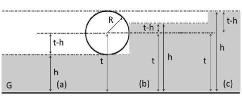
Typically, the configuration of a NW-FET is shown in Fig. 1(a), where the NW is separated from the gate by a dielectric slab of thickness . The capacitance formula given by Eq. (3) has been commonly used in the evaluation of back-gate capacitance of NW-FETs Wang et al. (2003); Duan et al. (2001); Javey et al. (2002). On the other hand, Eq. (3) is correct if only the entire space is a dielectric of permittivity . As a result it was noticed in several works that, for real devices, formula given by Eq. (3) is valid if the relative permittivity of the dielectric slab is replaced by an effective permittivity that is approximately half (more precisely 58%) of when the dielectric is silicone dioxide Wunnicke (2006); Ford et al. (2009).
In the present work we perform an extensive study by considering not only different dielectric slab thicknesses or embeddings but also different dielectric constants. Some of the present results have been previously reported in a recent conference paper Boldeiu et al. (2014). Two of those embeddings are depicted in Fig. 1(b) (the NW is more than half-buried by the dielectric) and Fig. 1(c) with the NW fully buried just below the dielectric-air interface. We will show that Eq. (3) may be used to describe the back-gate capacitance of the NW for arbitrary slab embeddings. This description of the capacitance is determined by that is the difference between the distance NW-gate and the dielectric thickness. Thus, if is constant, Eq. (3) is valid with an appropriate that depends not only on but also on . Deviation from this behavior occurs when the dielectric slab is thinner, i. e., . We further analyze capacitance changing with respect to dielectric thickness in order to assess the sensing capabilities of liquid levels in microfluidic systems. We have found that with respect to the dielectric thickness the capacitance characteristics have an S-like shape with three distinct regions. The capacitance varies almost linearly in the first region, slowly in the third one, and rapidly in the middle region that is located around the NW.
The paper has the following structure. In the second section we present the problem and the method of resolution. The third section is dedicated to the main results and the last section will summarize the conclusions.
II Preliminaries and the Method
Our problem resides in solving the Laplace equation with Dirichlet boundary conditions, i. e., a fixed potential on the surface of cylinder and with a grounded back-gate. The capacitance can be calculated numerically by a variety of methods including finite element methods Johnson (1987) or boundary element methods Poljak and Brebbia (2005). The boundary element method is the finite element version of the boundary integral method which comes from potential theory Kellog (1967). In the static limit metallic regions are considered to totally screen the electric fields thus those regions are equipotential regions. This is not valid when, instead of static fields, the electromagnetic fields are considered, such that metals have a finite dielectric permittivity at optical frequencies. Thus, for metallic nanostructures with features much smaller than the wavelength of the incoming electromagnetic wave the response of a metallic system is given by the same Laplace equation but with different boundary conditions (basically there are Neumann boundary conditions) Sandu et al. (2011); Sandu (2013). The method is a spectral approach to the boundary integral equation that turns out to obtain simultaneously also the electrostatic capacitance of metallic nanostructures Sandu et al. (2013).
Capacitance and the electrostatic response of finite cylinders have been studied in Sandu et al. (2013) and in Sandu (2014), respectively, where explicit expressions for both capacitance and electric polarizability of finite cylinders have been found. On the other hand, an infinite long cylinder with a grounded planar back-gate and homogeneously embedded in a dielectric of relative permittivity has also an explicit capacitance that is given by Eq. (3). One calculation procedure is based on the bipolar coordinates Boldeiu et al. (2014); Arfken (1970). In the usual setup with the NW perpendicular on the (x,y) plane, the bipolar coordinates given by
| (4) |
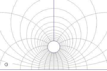
generate the equipotential surfaces and the field lines of a cylinder charged under a potential with respect to the grounded planar gate Boldeiu et al. (2014). The equation of the NW surface is , while the equation of the planar gate is = 0. We notice that the ratio from Fig. 1 is In the (x,y) plane the new coordinates (, are shown in Fig. 2. Thus, the surfaces = constant are cylinders that surround our NW Arfken (1970). They turn out to be equipotential surfaces of a charged cylinder including also the surface = 0 that is our planar gate. The surfaces = constant are also cylinders and define the field lines that start up normally on the NW and end up also normally on the planar gate Arfken (1970).
We have shown that in the case of electrostatic capacitance once the equipotential surfaces and field lines are known one can estimate straightforward the capacitance of the system Sandu et al. (2013). Accordingly, the capacitance of the back-gated NW is
| (5) |
where , , and are the Lamé coefficients of the transformation (4)
| (6) |
| (7) |
which is just Eq. (3) since . Similar formulae can be obtained for two non-concentric cylinders or for two parallel cylinders Boldeiu et al. (2014).
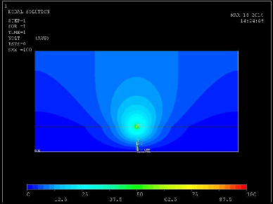
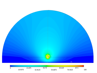
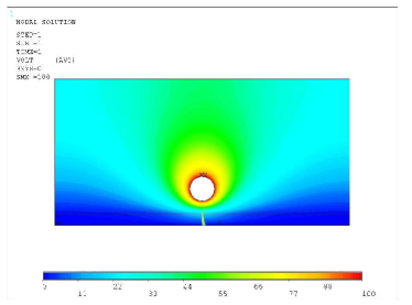
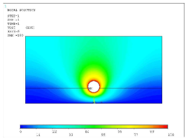
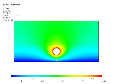
Slight modifications of the shapes of nanostructures induce minute changes on capacitance Sandu et al. (2013) or on higher excitations modes Sandu (2012); Sandu and Boldeiu (2014). On the other hand, the back-gated NWs are not infinitely long and have a certain degree of doping, effects that cannot be analytically quantified. Extensive numerical calculations have shown that with a doping as much as 5x1018 cm-3 and with an aspect ratio as large as 100 the behavior of the semiconductor NW is that of infinitely long metallic NW Khanal and Wu (2007). Furthermore, the capacitance of the back-gated NW with a finite but otherwise arbitrary thickness of the dielectric cannot have a readily analytic formula like that of the homogeneous case. Hence we invoke a fully numerical procedure to calculate the NW capacitance in various dielectric embeddings. Our calculations are based on ANSYS which is a finite element based multiphysics software program ans . In ANSYS there are several methods for computing the electrostatic capacitance of a metallic system. The first and the simplest method is a pure finite element method in a finite computation box, hence the equipotential surfaces are enforced to close on the boundaries of the computation box (Fig. 3a). Another method is the method that uses infinite boundary elements (Fig. 3b). As we can see from the figure the infinite boundary elements ensure a more physical appearance of the equipotential surfaces with respect to a finite computation box by considering the same computer overhead. Therefore, the second method is more accurate and faster in convergence than the first one. Nevertheless we have used the first method but we have tuned it with respect to the second one by making the results of the two methods be apart by less than 0.5%. The major reason for this choice was the fact that the first method is more suitable to be used in ANSYS scripts of repeated calculations.
III Results
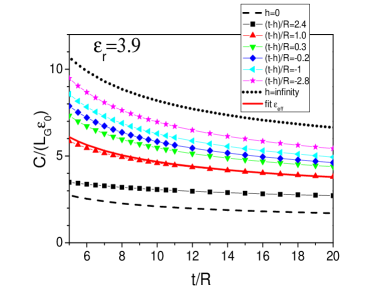
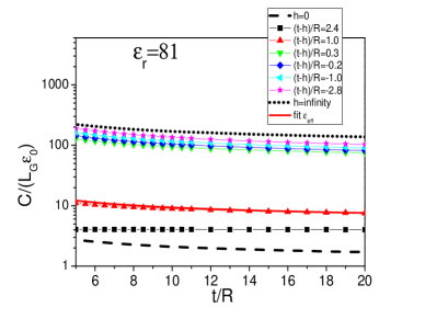
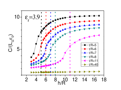
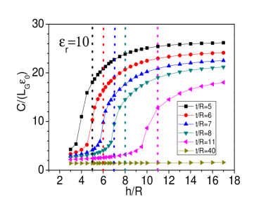
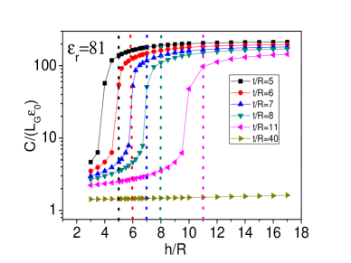
Our main results are presented in Figs. 4, 5, and 6. The dielectric constants considered in this work are (i. e. SiO, (a lower limit of high- dielectrics), and (the dielectric constant of water). In Fig. 4 we present the NW capacitance as a function of with 5 (the typical setting for a NW-FET) and with different dielectric embeddings. The level of dielectric embedding was established in such a way that is constant. In this setting the capacitance of the NWs shows good scaling properties according to Eq. (3) with an effective dielectric permittivity for each value of . The particular case =1, in which the dielectric separates the NW and the gate plane, is plotted with upward oriented triangles and is also fitted with an effective dielectric permittivity. The results of fitting are plotted with solid lines showing a quite good superposition on the calculated curves. The case =1 is the standard configuration of the NW-FET and was studied in Wunnicke (2006) where an effective permittivity was given. We have obtained a value . In addition, when the high- dielectric HfO2was used ( the effective permittivity was about 34% of that of the dielectric Wunnicke (2006). Our calculations indicate that the effective permittivities are 43 percent and 5.5 percent of permittivities of the dielectric with and , respectively. One can further notice that for varying between -1 and 1 the varies nonlinearly with respect to the variation of .
The scaling is still valid for dielectric permittivities as large as that of water in spite of the fact that at quite large dielectric constant the dielectrics should behave as a metal. Nevertheless the metallic behavior (manifested as strong screening) of the dielectric sets in when (i. e., the NW is well above the dielectric layer) and the scaling is no longer valid. One can also notice that at for both and the capacitance is almost constant, a feature of metallic behavior. Fig. 5 illustrates more clearly that only for (Fig. 5a) the dielectric screens the back gate hence the scaling described above cannot longer be valid. In addition, for dielectric embeddings that completely cover the NW the capacitance goes very slowly to the value of complete filling of the space with dielectric (Fig. 5c).
We will further analyze and discuss the previous scaling behavior for certain applications used to determine the dielectric thickness by electrical measurements using NW-FET. A potential application one can think of is the estimation of the liquid height in microfluidic systems. To keep the discussion as simple as possible we suppose that the surface of the NW is passivated and the liquid is totally wetting the NW surface. In Fig. 6 we plotted the NW capacitance with respect to thickness at various values of . In fact the curves plotted in Fig. 6 give information about discussed previously. The capacitance is -shaped with three distinct regions. For small thicknesses the capacitance varies linearly as it was expected on perturbative grounds. The size of this region increases but the slope of the curves decrease with the increase of . Hence, at the size of this linear region is significantly larger as one can see it from Fig. 6. In this region, in order to exploit its linearity for sensing, one has to trade off between the size of the linear region and the slope of capacitance with respect to dielectric thickness . By inspecting Fig. 6 it seems that ensures an optimum sensing in this region. The second region displays the largest capacitance variation with greater slopes for greater dielectric permittivities. The region spans approximately four NW radiuses around the NW center and can be used as a proximity sensor in which the capacitance increases considerably when the liquid levels are in the vicinity of the NW. Finally, the third region of deeper dielectric embedding the capacitance varies smoothly and saturates to its asymptotic value of total embedding.
IV Conclusions
In the present work we have studied the back-gate capacitance variation of a nanowire with respect to various levels of dielectric embedding. The standard configuration in the field effect transistor setting is that in which the dielectric separates the nanowire from the gate plane. It was previously shown that this standard geometric arrangement has a scaling behavior straightforwardly connected to the back-gated nanowire embedded in a homogeneous dielectric. The scaling is made with an effective dielectric constant that strongly depends on the permittivity of the dielectric. In our paper we have shown numerically that this scaling is valid for various degrees of dielectric embedding granted the fact that the difference between the dielectric thickness and the gate-nanowire distance is constant. The scaling is dependent on the difference between the dielectric thickness and the gate-nanowire distance and on the permittivity of the dielectric. However, the scaling is not valid for dielectric thicknesses much smaller than the distance nanowire-gate because of the dielectric screening. We further discuss this property for sensing purposes. Thus, we analyze the capacitance change with respect to dielectric thickness as an indicator of liquid height in microfluidic systems. The capacitance curves have an S-like shape with three regions. The first region is almost linear and might be optimum for sensing if the ratio between gate-nanowire distance and the nanowire radius is about 10. The second region which is of the size of two diameters around the center of the nanowire has the largest slope and can be used for sensors of proximity. The third region is rather unimportant since the capacitance in the region saturates slowly to its asymptotic value given by the embedding of the nanowire in a dielectric of infinite thickness.
Acknowledgements.
This work was supported by a grant of the Romanian National Authority for Scientific Research, CNCS – UEFISCDI, project number PNII-ID-PCCE-2011 -2-0069.References
- Lieber (2011) C. M. Lieber, MRS Bull. 36, 1052 (2011).
- Duan et al. (2013) X. Duan, T. M. Fu, J. Liu, and C. M. Lieber, Nano Today 8, 351 (2013).
- Timko et al. (2010) B. P. Timko, T. Cohen-Karni, Q. Qing, B. Tian, and C. M. Lieber, IEEE Trans. Nanotechnology 9, 269 (2010).
- Sze (1981) S. M. Sze, Physics of Semiconductor Devices (Wiley Inter-Science, New York, 1981), 2nd ed.
- Dayeh (2010) S. A. Dayeh, Semicond. Sci. Technol. 25, 024004 (2010).
- Wang et al. (2003) D. Wang, Q. Wang, A. Javey, R. Tu, H. Dai, H. K. P. C. McIntyre, T. Krishnamohan, and K. C. Saraswat, Appl. Phys. Lett. 83, 2432 (2003).
- Duan et al. (2001) X. Duan, Y. H. Y. Cui, J. Wang, and C. M. Lieber, Nature(London) 409, 66 (2001).
- Javey et al. (2002) A. Javey, H. Kim, M. Brink, Q. Wang, A. Ural, J. Guo, P. McIntyre, P. McEuen, M. Lundstrom, and H. Dai, Nature Materials 1, 241 (2002).
- Wunnicke (2006) O. Wunnicke, Appl. Phys. Lett. 89, 083102 (2006).
- Ford et al. (2009) A. C. Ford, J. C. Ho, Y. L. Chueh, Y. C. Tseng, Z. Fan, J. Guo, J. Bokor, and A. Javey, Nano Lett. 9, 360 (2009).
- Boldeiu et al. (2014) G. Boldeiu, V. Moagar-Poladian, and T. Sandu, in IEEE-International Semiconductor Conference (CAS) (Sinaia, Romania, 2014), pp. 273–276.
- Johnson (1987) C. Johnson, Numerical Solutions of Partial Differential Equations by Finite Element Method (Cambridge, University Press, Cambridge, UK, 1987).
- Poljak and Brebbia (2005) D. Poljak and C. A. Brebbia, Boundary Element Methods for Electrical Engineers (WIT, Boston, USA, 2005).
- Kellog (1967) O. D. Kellog, Foundations of Potential Theory (Springer-Verlag, Berlin, Heidelberg, New York, 1967).
- Sandu et al. (2011) T. Sandu, D. Vrinceanu, and E. Gheorghiu, Plasmonics 6, 407 (2011).
- Sandu (2013) T. Sandu, Plasmonics 8, 391 (2013).
- Sandu et al. (2013) T. Sandu, G. Boldeiu, and V. Moagar-Poladian, J. Appl. Phys 114, 224904 (2013).
- Sandu (2014) T. Sandu, Proceedings of the Romanian Academy, Series A 15, 338 (2014).
- Arfken (1970) G. Arfken, Mathematical Methods for Physicists (Academic Press, Orlando, Florida, 1970), 2nd ed.
- Sandu (2012) T. Sandu, Journal of Nanoparticle Research 14, 905 (2012).
- Sandu and Boldeiu (2014) T. Sandu and G. Boldeiu, Digest Journal of Nanomaterials and Biostructures 9, 1255 (2014).
- Khanal and Wu (2007) D. R. Khanal and J. Wu, Nano Lett. 7, 2778 (2007).
- (23) ANSYS® Academic Research, Release 12.1, Help System, Low- Frequency Electromagnetic Guide, ANSYS, Inc.